11.1 NATURAL NUMBERS
11.1.1 Basic Adder (Ripple-Carry Adder)
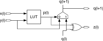
The structure of an n-digit ripple-carry adder is shown in Figure 11.1. The full adder (FA) cell calculates q(i + 1) and z(i) as a function of x(i), y(i), and q(i), according to the iteration body of Algorithm 4.1:

Figure 11.1 Basic adder.
Let CFA and TFA be the cost and the computation time of an FA cell. The cost and computation time of an n-digit basic adder are equal to
Examples 11.1
- In base 2 the FA equations (11.1) are
(∨: or function, ⊕ : xor function).
- In base 10 the FA equations are
The decimal digits can be represented as 4-bit binary numbers (BCD—binary-coded decimal representation) so that a decimal full adder is a 9-input, 5-output binary circuit. It can be implemented using classical methods and tools of combinational logic synthesis. Another option is to decompose it further on. The following algorithm computes (11.4):
s:=x(i)+y(i)+q(i);
if s>9 then z(i):=(s+6) mod 16; q(i+1):=1; else z(i):=s;
q(i + 1):=0; end if;
The corresponding circuit (Figure 11.2) is made up of a 4-bit binary adder that computes s (a 5-bit number), a 4-input 1-output combinational circuit that computes and another 4-bit binary adder that computes the BCD 4-bit expression of the sum
![]()
![]()
so that

Observe that in the preceding example z1 and z3 can be computed by half-adder (HA) cells whose equations are deduced from (11.3) substituting one of the operands, say, y(i), by zero:
![]()
More generally (base B), the half-adder equations are
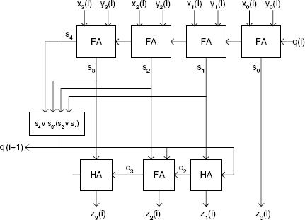
Figure 11.2 Decimal full adder.
11.1.2 Carry-Chain Adder
The structure of an n-digit adder with separate carry calculation is shown in Figure 11.3. It is based on Algorithm 4.2. The G-P (generate–propagate) cell calculates the generate and propagate functions (4.1), that is,
The Cy.Ch. (carry-chain) cell computes the next carry, that is,
![]()
so that g(i) generates a carry, whatever happened upstream in the carry chain, and p(i) propagates the carry from level i – 1. The mod B sum cell calculates
![]()
Let CGP and TGP, CCy.Ch. and TCy.Ch., and Csum and Tsum be the cost and the computation time of a G-P cell, Cy.Ch. cell, and mod B sum cell, respectively. The cost and computation time of an n-digit carry-chain adder are equal to
As regards the computation time, the critical path is shaded in Figure 11.3. It has been assumed that Tsum > TCy.Ch..

Figure 11.3 Carry-chain adder.
Another interesting time is the delay Tcarry(n) from q(0) to q(n) assuming that all propagate and generate functions have already been calculated:
Comments 11.1
- The carry-chain cells are binary circuits while the generate–propagate and the mod B sum cells are B-ary ones.
- The carry-chain cell is functionally equivalent to a 2-to-1 binary multiplexer (Figure 11.4a), so that, according to (11.7), the per-digit delay of a carry-chain adder is equal to the delay Tmux2−1 of a 2-to-1 binary multiplexer, whatever the base B. Furthermore (Comment 4.1.(2)) the definition of the generate function can be relaxed:

If B = 2 and the carry-chain cell of Figure 11.4a is used, then p(i) = x(i) ⊕ y(i) and g(i) can be chosen equal to for example, y(i). The corresponding n-bit adder is shown in Figure 10.1. Its cost and computation time are given by (10.1).
- Another way to synthesize the carry-chain cell—the Manchester carry chain—is shown in Figure 11.4b. First observe that the complement of the carries is computed. It works as follows: the output node (the complement of q(i + 1)) is precharged when the synchronization signal clk is equal to 0; when clk = 1 the output node is discharged if either p(i) = 1 and the preceding node (the complement of q(i)) has been discharged, or if g(i) = 1. In order that it works properly g(i) and p(i) should not be equal to 1 at the same time so that the definition of g cannot be relaxed as in the preceding case.

Figure 11.4 Carry-chain cells.
Example 11.2 (Complete VHDL source code available). Generate a generic n-digit base-B carry-chain adder:
 entity example11_2 is
 port (
   x, y: in digit_vector(n-1 downto 0);
   c_in: in std_logic;
   z: out digit_vector(n-1 downto 0);
   c_out: out std_logic
 );
 end example11_2;

 architecture circuit of example11_2 is
   signal p, g: std_logic_vector(n-1 downto 0);
   signal q: std_logic_vector(n downto 0);
 begin
   q(0)<=c_in;
   iterative_step: for i in 0 to n-1 generate
     p(i)<=‘1’ when x(i)+y(i)=B-1 else ‘0’;
     g(i)<=‘1’ when x(i)+y(i)>B-1 else‘0’;
     with p(i) select q(i+1)<=q(i) when ‘1’, g(i) when others;
     z(i)<=(x(i)+y(i)+conv_integer(q(i))) mod B;
   end generate;
   c_out<=q(n);
 end circuit;
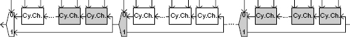
11.1.3 Carry-Skip Adder
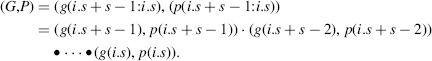
Consider a group of s successive cells within a carry chain (Figure 11.5). If all propagate functions p(i.s), p(i.s + 1), …, p(i.s + s − 1) within the group are equal to 1 then q(i.s + s) = q(i.s), and the carry q(i.s) is said to be propagated through the group. In the contrary case, there is at least one cell, say, number i.s + j, such that p(i.s + j) = 0 so that q(i.s + j + 1) = g(i.s + j). Assume that cell number i.s + j is the last one such that p(i.s + j) = 0 and p(i.s + j + 1) = … = p(i.s + s − 1) = 1. Then q(i.s + s) = g(i.s + j), and the carry q(i.s + s) is said to be locally computed within the group.

Figure 11.5 An s-bit carry chain.
An n-bit carry-skip carry chain is made up of n/s s-bit carry chains interconnected through 2-to-1 multiplexers (Figures 11.6 and 11.7). Besides the generate and propagate functions, the generalized propagate functions p(i.s + s − 1:i.s) = p(i.s + s − 1) .…. p(i.s + 1).p(i.s) must also be computed.
The structure of a carry-skip adder is shown in Figure 11.8. It is made up of n G-P cells, n Cy.Ch. cells, n mod B sum cells, n/s 2-to-1 multiplexers, and n/s s-input AND gates (or any equivalent circuit) for computing p(i.s + s − 1:i.s). Its cost and computation time are equal to
The critical path of the carry chain is shaded in Figure 11.7. It has been assumed that s.Tcy.ch. > TAND(s) and Tsum > Tcy.ch. + Tmux2−1, so that in the first group p(s − 1:0) is computed in parallel with the multiplexer inputs, and in the last group the critical path is from q(n − s) to z(n − 1) through s − 1 Cy.Ch. cells and one mod B sum cell.
As before another interesting time is the delay Tcarry(n,s) from q(0) to q(n) assuming that all propagate, generate, and generalized propagate functions have already been calculated:
Comments 11.2
- For great values of n and s the computation time (11.9) is roughly equal to (n/s).Tmux2−1 + 2.s.TCy.Ch.. It must be compared with (11.7), that is, (approximately), n.TCy.Ch.. The computation time reduction is due to the fact that the locally generated carries are calculated in parallel.
Figure 11.6 Carry chain: s-bit group.
- The s rightmost Cy.Ch. cells of Figure 11.7 belong to the critical path, so that the first multiplexer should be deleted, unless the corresponding adder is used as a building block for larger adders.

Multilevel carry-skip adders can be defined. For example, each s-bit carry chain in Figure 11.7 could in turn be substituted by s/t t-bit carry chains. The corresponding delay Tcarry(n, s, t) from q(0) to q(n) assuming that all propagate, generate, and generalized propagate functions have already been calculated is
![]()
so that, according to (11.10),
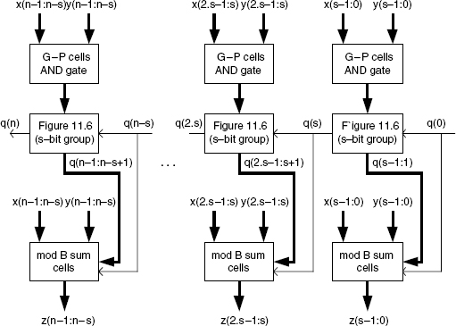
Figure 11.8 Carry-skip adder structure.
and so on. In particular, if n = sm,
that is,
If the computation time of every generalized propagation function is assumed to be shorter than the propagation time of the corresponding (partial) carry chain, then the delay of the complete adder is equal to (11.14) plus the delay of a G-P cell and of a mod B sum cell, that is, a logarithmic delay.
Example 11.3 (Complete VHDL source code available). Generate a generic n-digit base-B carry-skip adder:
 entity carry_skip is
 port(
   x, y: in digit_vector(s-1 downto 0);
   c_in: in std_logic;
   c_out: out std_logic_vector(s downto 1)
 );
 end carry_skip;

 architecture circuit of carry_skip is
   signal p, g: std_logic_vector(s-1 downto 0);
   signal generalized_p: std_logic;
   signal q: std_logic_vector(s downto 0);
 begin
   q(0)<=c_in;
   iterative_step: for i in 0 to s-1 generate
     p(i)<=‘1’ when x(i)+y(i)=B-1 else ‘0’;
     g(i)<=‘1’ when x(i)+y(i)>B-1 else‘0’;
     with p(i) select q(i+1)<=q(i) when ‘1’, g(i) when others;
   end generate;
   process(p)
     variable accumulator: std_logic;
   begin
     accumulator:=p(0);
     for i in 1 to s-1 loop accumulator:=accumulator and p(i);
     end loop;
     generalized_p<=accumulator;
   end process;
   with generalized p select c_out(s)<=c_in when ‘1’, q(s) when
   others;
   carries: for i in 1 to s-1 generate c_out(i)<=q(i);
   end generate;
 end circuit;

 entity example11_3 is
 port(
   x, y: in digit_vector(n-1 downto 0);
   c_in: in std_logic;
   z: out digit_vector(n-1 downto 0);
   c_out: out std_logic
 );
 end example11_3;

 architecture circuit of example11_3 is
   component carry_skip…end component;
   signal q: std_logic_vector(n downto 0);
 begin
   q(0)<=c_in;
   ext_iteration: for i in 0 to n_div_s-1 generate
     csa_carry_chain: carry_skip port map(x(i*s+s-1 downto
     *s), y(i*s+s-1 downto i*s), q(i*s), q(i*s+s downto
     i*s+1));
     int_iteration: for j in 0 to s-1 generate
       z(i*s+j)<=(x(i*s+j)+y(i*s+j)+conv_integer(q(i*s+j)))
       mod B;
     end generate;
   end generate;
   c_out<=q(n);
 end circuit;
11.1.4 Optimization of Carry-Skip Adders
Assume that in the carry-skip adder of Figure 11.7 the last carry of group number j, namely, q(j.s + s − 1), has been generated or killed (Example 10.6) within the first cell of group number i and propagated toward group number j. Then the computation time of q(j.s + s − 1), assuming that all the propagate, generate, and generalized propagate functions have already been calculated, is equal to
![]()
In particular (worst case), if j = n/s − 1 and i = 0, then
The theoretical minimum value of t(0, n/s − 1) is obtained when 2.s.TCy.Ch.. = n/s.Tmux2−1, that is,
where
The corresponding value of (11.15) is approximately
A better solution is obtained if the groups are allowed to have different sizes. Assume that the group sizes are s0, s1, …, sk − 1, where s0 + s1 + … + sk − 1 = n. Then the computation of the last carry of group number j, assuming that it has been generated or killed within the first cell of group number i , and propagated toward group number j, is equal to
The corresponding optimization problem can be stated as follows:
define k, s0, s1, …, sk − 1, such that the cost function
![]()
be minimum and
Obviously it's a complex problem. Nevertheless, an interesting solution is deduced from the following observation: if the difference j − i is big (it means that group i is one of the first ones and group j one of the last ones), then si and sj should be small; conversely, if the difference j − i is small (it could mean that groups i and j are close to the center), then si and sj are allowed to have bigger values. Thus choose
(assuming that k is even). Furthermore, in order that the values of the computation times t(0, k − 1), t(1, k − 2), …, t(k/2 − 1, k/2) be equal, then
where α is defined by (11.17). The value of s0 is deduced from (11.20), (11.21), and (11.22):
![]()
and
The corresponding value of t(0,k − 1) is approximately equal to
In order to minimize (11.24), the value of k is chosen in such a way that
![]()
that is, using (11.17)
so that
Substituting k by (11.26) in (11.23) yields
According to (11.19), (11.21), and (11.17) the value of the carry computation time is
![]()
and, for k great enough,
Thus the variable size approach allows the reduction of the delay by a factor 21/2 (compare (11.18) and (11.28)).
Comment 11.3 Generally, Tmux2-1 and TCy.Ch.. have the same order of magnitude, so that α ≅ 1; s0 should be chosen equal to 1 and k to approximately ((1 + 4.n)1/2 − 1) in order that (11.23) be satisfied with s0 = α = 1.
Example 11.4 With n = 64 and s0 = α = 1, the number of groups is equal to ((1 + 4.64)1/2 − 1) ≅ 15. A possible choice is
![]()
Calculating some carry computation times (11.19):
The fixed group-size approach, with α = 1, gives the following results:
![]()
Choose, for example, ten groups, six of 6 digits and four of 7 digits. Then (11.15)
![]()
which is significantly greater than the above values with heterogeneous size blocks.
11.1.5 Base-Bs Adder
In a base-Bs adder, every slice of Figure 11.3 is replaced by the circuit of Figure 11.9. The combinational circuit computes the generalized generate and propagate functions (Definitions 4.1)
Its cost and computer time are equal to

Figure 11.9 Base-Bs adder cell.
The computation of G and P can be performed with the dot operation (Definitions 4.1):
Let Cdot and Tdot be the cost and computation time of a dot operator. As the dot operation is associative, the computation can be executed by a (log2 s)-level tree of (s − 1) dot operators, so that
![]()
and, using those values in (11.30),
11.1.6 Carry-Select Adder
Once again the adder is decomposed into n/s groups of s adder steps. For every group a conditional carry chain is generated (Figure 11.10). It computes the functions q0(i.s + j) and q1(i.s + j) according to the canonical expansion
that is, the carry is equal to q0(i.s + j) when q(i.s) = 0, and to q1(i.s + j) when q(i.s) = 1.
An s-digit carry-select adder cell is shown in Figure 11.11. It is made up of an s-bit conditional carry chain, s 2-to-1 binary multiplexers that select the actual carry value (either q0(i.s + j) or q1(i.s + j)) as a function of q(i.s), as well as the G-P and mod B sum cells.
The complete adder structure is shown in Figure 11.12. Its cost and computation time (see the shaded blocks) are equal to
Multilevel carry-select adders can be defined. With two s-bit conditional carry chains (Figure 11.10), as well as two s-bit 2-to-1 multiplexers, a (2.s)-bit conditional carry chain can be generated (Figure 11.13). Assume that
![]()
Then replace in the preceding equation q(s) by not(q(0)).q0(s) + q(0).q1(s):

thus
![]()
Let Tcond.carry(s) be the computation time of a conditional carry chain. Then, according to Figure 11.13,

Figure 11.10 An s-bit conditional carry chain.

Figure 11.11 An s-bit carry-select carry chain.

Figure 11.12 Carry-select adder.
A recursive use of the decomposition of Figure 11.13 allows one to generate a (2p.s)-bit conditional carry chain whose computation time is equal to
![]()
that is,
The computation time of the corresponding n-digit adder is equal to (11.35) plus the delay of one G-P cell and of one mod B sum cell—a logarithmic behavior.

Figure 11.13 A (2.s)-bit conditional carry chain.
Example 11.5 (Complete VHDL source code available). Generate a generic n-digit base-B carry-select adder:
 entity carry_select is
 port (
   x, y: in digit_vector(s-1 downto 0);
   c_in: in std_logic;
   c_out: out std_logic_vector(s downto 1)
  );
 end carry_select;

 architecture circuit of carry_select is
   signal p, g: std_logic_vector(s-1 downto 0);
   signal q0, q1: std_logic_vector(s downto 0);
 begin
   q0(0)<=‘0’; q1(0)<=‘1’;
   iterative_step: for i in 0 to s-1 generate
     p(i)<=‘1’ when x(i)+y(i)=B-1 else ‘0’;
     g(i)<=‘1’ when x(i)+y(i)>B-1 else‘0’;
     with p(i) select q0(i+1)<=q0(i) when ‘1’, g(i) when
     others;
     with p(i) select q1(i+1)<=q1(i) when ‘1’, g(i) when
     others;
     with c_in select c_out(i+1)<=q0(i+1) when ‘0’, q1(i+1)
     when others;
   end generate;
 end circuit;

 entity example11_5 is
 port (
   x, y: in digit_vector(n-1 downto 0);
   c_in: in std_logic;
   z: out digit_vector(n-1 downto 0);
   c_out: out std_logic
 );
 end example11_5;

 architecture circuit of example11_5 is
   component carry_select …
   signal q: std_logic_vector(n downto 0);
 begin
  <substitute the carry_skip component by the carry_select
  one in example11_3>
end circuit;
11.1.7 Optimization of Carry-Select Adders
In the carry-select adder of Figure 11.12, assuming that all the generate and propagate functions have been previously computed, the computation time of the carries of group number j is equal to
In particular (worst case),
The minimum value of (11.37) is obtained when s.TCy.Ch.. = n/s.Tmux2-1, that is, when
where α is defined by (11.17). The corresponding value of (11.37) is approximately equal to
As for carry-skip adders, a better solution is obtained if the groups are allowed to have different sizes, say, s0, s1, …, sk − 1, where s0 + s1 + … + sk − 1 = n. Every multiplexer receives two types of input signals: the locally generated carries (q0 and q1) and the output carry of the preceding group whose value controls the selection of either q0 or q1. If all groups have the same size, then the locally generated carries of the latest groups are available much sooner than the control signal propagated all along the previous groups. In order that both types of signals arrive more or less at the same time, the latest blocks should be longer than the first ones. For group number j the computation time of the control signal is
and the computation time of the local carries is
Choosing sj in such a way that
![]()
that is,
where α is defined by (11.17), the computation time of q(j) is equal to

Compute the value of s0 such that both (11.42) and (11.20) are satisfied:
![]()
and
According to (11.42), (11.43), and (11.44),
whose minimum value is obtained when
![]()
that is,
Substituting k by the preceding value in (11.44) yields
According to (11.42), (11.43), (11.46), and (11.47),
The delay has been reduced by a factor of 21/2 (compare (11.38) with (11.47)).
Comment 11.4 Generally, Tmux2−1 and TCy.Ch.. have the same order of magnitude, so that α ≅ 1; s0 should be chosen equal to 1 and k to approximately ![]()
![]() in order that (11.44) be satisfied with s0 = α = 1.
in order that (11.44) be satisfied with s0 = α = 1.
Example 11.6 With n = 64 and s0 = α = 1, the number of groups is equal to ![]() A possible choice is
A possible choice is
![]()
According to (11.43),
![]()
The fixed group-size approach, with α = 1, gives the following results:
![]()
Thus (11.39)
![]()
11.1.8 Carry-Lookahead Adders (CLAs)
Figure 11.14 shows an n-bit carry-lookahead carry chain, based on the recursive algorithm 4.8. It is made up of two types of components:
the dot component implements equations (4.5);
the carry component implements equations (4.6), that is,
![]()
Let Cdot(s) and Tdot(s) be the cost and delay of an s-bit dot component, and Ccarry and Tcarry the cost and delay of a circuit computing the switching function f = x ∨ y.z. The cost Ccla(n) and the computation time Tcla(n) of the n-bit carry-lookahead carry chain are equal to
A recursive use of equations (11.49) demonstrates that

Figure 11.14 n-bit carry-lookahead carry chain.
In particular, if n = sk then, as Ccla(1) = Ccarry and Tcla(1) = Tcarry,
The computation time of the corresponding n-digit adder is equal to (11.51) plus the delay of a G-P cell and of a mod B sum cell: that is, a logarithmic computation time.
Example 11.7 (Complete VHDL source code available.) Generate a generic two-level n-digit base-B carry-lookahead adder. The following model is based on Figure 11.14. In order to obtain a three-level carry-lookahead adder, the behavioral description of the (n/s)-bit carry chain should be replaced by a structural description based on Figure 11.14 with n substituted by n/s, and so on.
 entity cla_carry_chain is
 port (
   g, p: in std_logic_vector(n-1 downto 0);
   c_in: in std_logic;
   c_out: out std_logic_vector(n downto 0)
  );
  end cla_carry_chain;

  architecture circuit of cla_carry_chain is
    component dot…end component;
    component carry…end component;
    signal q: std_logic_vector(n downto 0);
    signal gg, pp: std_logic_vector(n-1 downto 0);
    signal ggg, ppp, generalized_ggg, generalized_ppp:
    std_logic_vector(n_div_s-1 downto 0);
    signal qqq: std_logic_vector(n_div_s downto 1);
  begin
    dot_iteration: for i in 0 to n_div_s-1 generate
      dot_instantiation: dot port map(g(i*s+s-1 downto i*s),
      p(i*s+s-1 downto i*s), gg(i*s+s-1 downto i*s),pp(i*s+s-1
      downto i*s));
    end generate;
    input_connections: for i in 0 to n_div_s-1 generate
      ggg(i)<=gg(i*s+s-1); ppp(i)<=pp(i*s+s-1);
   end  generate;
   ---------------------------------------------------------------------------------
   --behavioral description of an (n_div_s)-bit cla carry
   --chain:
   generalized_ggg(0)<=ggg(0); generalized_ppp(0)<=ppp(0);
   cla_carry_chain_description: for i in 1 to n_div_s-1 generate
    qqq(i)<=generalized_ggg(i-1) or (generalized_ppp(i-1) and
    c_in);
    dot_operation(ggg(i), ppp(i),
    generalized_ggg(i-1), generalized_ppp(i-1),
    generalized_ggg(i), generalized_ppp(i));
   end generate;
   qqq(n_div_s)<=generalized_ggg(n_div_s-1) or
   (generalized_ppp(n_div_s-1) and c_in);
  -----------------------------------------------------------------------------------
 output_connections: for i in 1 to s generate
  q(i*s)<=qqq(i);
 end generate;
 q(0)<=c_in;
 carry_iteration: for i in 0 to s-1 generate
  carry_instantiation: carry port map(gg(i*s + s-2 downto i*s),
   pp(i*s+s-2 downto i*s), q(i*s), q(i*s+s-1 downto i*s+1));
  end generate;
  output_carries_iteration: for i in 0 to s**2 generate
   c_out(i)<=q(i);
  end generate;
 end circuit;

 entity example11_7 is
 port (
  x, y: in digit_vector(n-1 downto 0);
  c_in: instd_logic;
  z: out digit_vector(n-1 downto 0);
  c_out: out std_logic
 );
 end example11_7;

 architecture circuit of example11_7 is
  component cla_carry_chain…end component;
  signal p, g: std_logic_vector(n-1 downto 0);
  signal q: std_logic_vector(n downto 0);
 begin
  iterative_step: for i in 0 to n-1 generate
   p(i)<=‘1’ when x(i)+y(i)=B-1 else ‘0’;
   g(i)<=‘1’ when x(i)+y(i)>B-1 else‘0’;
   z(i)<=(x(i)+y(i)+conv_integer(q(i))) mod B;
  end generate;
  cla_carry_chain_instantiation: cla_carry_chain port map(g, p,
  c_in, q);
  c_out<=q(n);
 end circuit;
Definition 11.1 A carry-lookahead generator (Figure 11.15a) is a (2.s + 1)-input (s + 1)-output combinational circuit equivalent to the circuit of Figure 11.15b. It computes the following switching functions:

Figure 11.15 Carry-lookahead generator.

An n-bit carry-lookahead carry chain made up of carry-lookahead generators is shown in Figure 11.16 (just another way to draw the circuit of Figure 11.14).
Example 11.8 Let n = 16, s = 4, that is, n/s = 4. The CLA equations can be written


Figure 11.16 An n-bit carry-lookahead carry chain (second version).

The complete circuit is shown in Figure 11.17.
Definition 11.2 An augmented full adder (AFA), whose symbol is shown in Figure 11.18, calculates g(i), p(i), and z(i) as a function of x(i), y(i), and q(i):

Carry-lookahead generators and augmented full adders are the building blocks for synthesizing carry-lookahead adders.
Example 11.9 The circuit of Figure 11.19 is an s2-digit carry-lookahead adder.
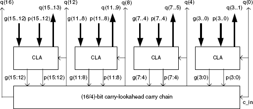
Figure 11.17 A 16-bit carry-lookahead carry-chain.

Figure 11.18 Augmented full adder.

Figure 11.19 An s2-digit carry-lookahead adder.
11.1.9 Prefix Adders
An n-bit prefix carry chain, based on the recursive algorithm 4.5 (BRE1982), is shown in figure 11.20. It is made up of components implementing the associative dot operation (Definitions 4.1), so that (4.5)
![]()
An n-bit prefix carry chain generates all the generalized generate and propagate functions of type g(i:0) and p(i:0), respectively. They have been underlined in Figure 11.20.
Let Cdot and Tdot be the cost and delay of the dot operator. According to Figure 11.20, the cost and computation time of an n-bit prefix carry chain (a Brent–Kung carry chain) are equal to
A recursive use of equations (11.52) yields

Figure 11.20 An n-bit Brent–Kung prefix carry chain.
In particular, if n = 2k+1 then

Comment 11.5 According to (11.54), TBrent–Kung(4) = 3.Tdot. It corresponds to the following scheduled algorithm:
- (g(3:2), p(3:2)): = (g(3), p(3)) • (g(2), p(2)); (g(1:0), p(1:0)): = (g(1), p(1)) • (g(0), p(0));
- (g(3:0), p(3:0)): = (g(3:2), p(3:2)) • (g(1:0), p(1:0));
- (g(2:0), p(2:0)): = (g(2), p(2)) • (g(1:0), p(1:0));
Nevertheless, the operations of cycles 2 and 3 could be executed in parallel, so that TBrent–Kung(4) = 2.Tdot. More generally,
In order to get the carries, an additional carry component (Figure 11.15b) should be added for computing
![]()
Example 11.10 (Complete VHDL source code available.) Generate a generic n-digit Brent-Kung base-B prefix adder. The following model is based on Figure 11.20.
entity prefix_2 is…
…
entity prefix_n_div_2 is…

entity prefix_n is
port (
  g, p: in std_logic_vector(n-1 downto 0);
  gg, pp: out std_logic_vector(n-1 downto 0)
);
end prefix_n;

 architecture circuit of prefix_n is
   component prefix_n_div_2…end component;
   signal a, b, aa, bb: std_logic_vector(n_div_2-1 downto 0);
 begin
   first_iteration: for i in 0 to n_div_2-1 generate
      dot_operation(g(2*i+1), p(2*i+1), g(2*i), p(2*i), a(i),
      b(i));
    end generate;
    component_instantiation: prefix_n_div_2 port map (a, b, aa,
    bb);
    second_iteration: for i in 1 to n_div_2-1 generate
        dot_operation(g(2*i), p(2*i), aa(i-1), bb(i-1), gg(2*i),
      pp(2*i));
    end generate;
    gg(0)<=g(0); pp(0)<=p(0);
    third_iteration: for i in 0 to n_div_2-1 generate
      gg(2*i+1)<=a(i); pp(2*i+1)<=b(i);
    end generate;
 end circuit;

 entity example11_10 is
 port (
   x, y: in digit_vector(n-1 downto 0);
   c_in: in std_logic;
   z: out digit_vector(n-1 downto 0);
   c_out: out std_logic
 );
 end example11_10;


 architecture circuit of example11_10 is
   component prefix_n…end component;
   signal p, g, pp, gg: std_logic_vector(n-1 downto 0);
   signal q: std_logic_vector(n downto 0);
 begin
   q(0)<=c_in;
   iterative_step: for i in 0 to n-1 generate
     p(i)<=‘1’ when x(i)+y(i)=B-1 else ‘0’;
     g(i)<=‘1’ when x(i)+y(i)>B-1 else‘0’;
     z(i)<=(x(i)+y(i)+conv_integer(q(i))) mod B;
  end generate;
  component_instantiation: prefix_n port map(g, p, gg, pp);
  carry_computation: for i in 1 to n generate
    q(i)<=gg(i-1) or (pp(i-1) and q(i-1));
  end generate;
  c_out<=q(n);
end circuit;
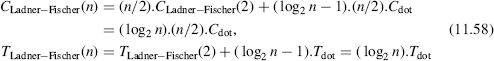
Another n-bit prefix carry chain, based on the recursive algorithm 4.6 ([LAD1980]), is shown in Figure 11.21.
Let Cdot and Tdot be the cost and delay of the dot operator. According to Figure 11.21 the cost and computation time of an n-bit prefix carry chain (a Ladner–Fischer carry chain) are equal to

Figure 11.21 An n-bit Ladner–Fischer prefix carry chain.
A recursive use of equations (11.56) yields
In particular, if n = 2k+1 then
Comments 11.6
- Several types of adders have been analyzed. As regards their cost and computation time, they can be classified into three groups:
- The ripple-carry and the carry-chain adders have O(n) cost and computation time, and the same occurs with the slice-based structures (carry-skip, base-Bs, carry-select) if s (the slice size) is a previously defined constant.
- In the case of the carry-skip and carry-select adders, the value of s can be optimized (Sections 11.1.4 and 11.1.7). Furthermore, the groups can have different sizes. Then the cost is O(n) and the computation time O(n1/2).
- The carry-lookahead and the prefix adders have O(n) cost (or even O(n.log(n)) and O(log(n)) computation time.
- Other parallel-prefix structures have been proposed, including [KOG1973], [HAN1987], and [SUG1990], all of them characterized by a logarithmic computation time.
11.1.10 FPGA Implementation of Adders
11.1.10.1 Carry-Chain Adders
FPGAs generally contain dedicated computation resources for generating fast adders. As an example, the Virtex-family programmable arrays (Chapter 9) include logic gates and multiplexers that, along with the general-purpose look-up tables, allow one to build effective carry-chain adders. The basic adder cell (Figure 11.22) allows implementation of the ripple adder of Figure 10.1. The carry chain is made up of multiplexers belonging to adjacent configurable blocks. The look-up table is used for implementing the exclusive-or function:
![]()
The computation time Tadder(n) of an n-bit adder is equal to
where tLUT is the computation delay of a general-purpose look-up table, tmux-cy the delay of a dedicated multiplexer along with the delay of the connection to the next adjacent block, and tXOR2 the delay of the 2-input XOR gate. It has been assumed that tXOR2 > tmux-cy. The delay from q(0) to q(n), assuming that all p(i) functions have already been calculated, is
Every slice of the Virtex family includes two cells so that the cost Cadder(n) of an n-bit adder is equal to
The computation time tLUT of a look-up table, as well as the average propagation time tconnection of a general-purpose connection, are much longer than tmux-cy (the delay of a dedicated multiplexer plus the connection to the next adjacent block). As a consequence, techniques such as the carry-lookahead or prefix adders, based on more complex computation resources (carry-lookahead generator, dot operation) and connection schemes, are generally inefficient. However, the carry-skip and carry-select techniques can be used. As an example, the FPGA implementation of carry-skip adders is analyzed in the next section.
11.1.10.2 Carry-Skip Adders
A key point in order to get fast circuits is the use of dedicated carry-logic multiplexers for any iterative subcircuit belonging to one of the critical paths. In the case of a carry-skip carry chain, both the circuits computing p(i.s + s-1:i.s) in every group (Figure 11.6) and the carry-skip multiplexers (shaded in Figure 11.7) can be implemented with carry-logic multiplexers. The computation of p(i.s + s − 1:i.s) is performed by the circuit of Figure 11.23. The look-up tables compute

Figure 11.23 Computation of p(i.s + s − 1:i.s).
p(i.s).p(i.s + 1) = (x(i.s) xor y(i.s)).(x(i.s + 1) xor y(i.s + 1)),
p(i.s + 2).p(i.s + 3) = (x(i.s + 2) xor y(i.s + 2)).(x(i.s + 3) xor y(i.s + 3)),
and so on.
The corresponding cost and delay are equal to
The multiplexers that select the output carry of every group—the so-called carry-skip multiplexers—belong to the critical path of the circuit, so that they must be implemented with dedicated carry multiplexers, as shown in Figure 11.24, where qq(i.s) is the carry locally generated by group number i − 1. Observe that the connection of p(i.s + s − 1:i.s) to the internal multiplexer must be done through the look-up table. The corresponding cost and propagation time are, respectively, equal to

Figure 11.24 Carry-skip multiplexers.
The implementation of an s-bit group of the adder is shown in figure 11.25. Its cost and delay are equal to
The complete circuit architecture is shown in Figure 11.26. The cost and computation time of an n-bit s-group carry-skip adder are equal to

As mentioned earlier (Comment 11.2(2)), the first carry-skip multiplexer is not necessary unless the adder is used as a building block for generating larger adders.

According to (11.65) the shortest theoretical delay is obtained when 2.s + n/s or 1,5.s + n/s is minimum, that is, when
11.1.10.3 Experimental Results
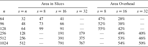
Several adders have been implemented [BIO2003] within a Spartan II-family FPGA. The synthesis was performed with the Xilinx Synthesis Technology (XST) and the physical implementation with the Xilinx ISE (Integrated System Environment) Version 5.1. In order to take advantage of the resources, the design was implemented instantiating the low-level FPGA components and using relative placement & routing (RPR).
The results are summarized in Table 11.1. The first column (s = n) gives the delay of a traditional adder. The last column gives the frequency increase of the fastest adder with respect to the traditional one. Additionally, Table 11.2 gives the area expressed in terms of FPGA slices.
Thanks to the use of the dedicated carry-logic circuitry for all blocks included within the critical path, the frequency increase for long-operand adders is substantial: more than 500% for a 1024-bit adder.
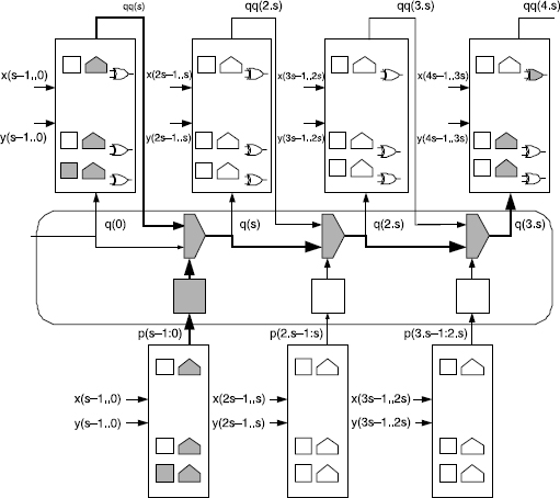
Figure 11.26 Complete carry-skip adder.
11.1.11 Long-Operand Adders
In the case of long-operand additions, the n-digit operands can be split down into s-digit groups and the addition computed according to Algorithm 4.10. The complete circuit is made up of an s-digit adder (procedure natural_addition of algorithm 4.10), connection resources giving access to the s-digit groups, a D-flip-flop that stores the carries (q in Algorithm 4.10), and a control unit whose kernel is an (n/s)-state counter. An example was seen in Chapter 10 (Example 10.4), where the access to the successive groups was through (n/s)-to-1 s-bit multiplexers.
TABLE 11.1 Experimental Results: Delay

TABLE 11.2 Experimental Results: Area
11.1.12 Multioperand Adders
11.1.12.1 Sequential Multioperand Adders
In order to compute z = x(0) + x(1) + … + x(m − 1), where every x(i) is a natural number, Algorithm 4.11 can be used. The corresponding sequential circuit is made up of an n-digit adder, an n-digit register, and a control unit; furthermore, some kind of connection resource (equivalent to an m-to-1 n-digit multiplexer) must be used in order to enter the m operands.
Example 11.11 (Complete VHDL code available.) Generate a generic m-operand n-digit adder. The circuit is shown in Figure 11.27.
The corresponding VHDL description (B = 2) is the following one:
 entity example11_11 is
 port (
   x: in operands;
   clk, start, reset: in std_logic;
   done: out std_logic;
   z: inout std_logic_vector(n-1 downto 0)
 );
 end example11_11;

  architecture circuit of example11_11 is
    signal adder_out, op_1: std_logic_vector(n-1 downto 0);
    signal operand_select: std_logic_vector(logm-1 downto 0);
    signal load, clear: std_logic;
    subtype state is integer range -3 to m;
    signal current_state: state;
  begin
    --data path:
    op_1<=x(conv_integer(operand_select));
    adder_out<=op_1+z;
    process(clk)
    begin
      if clear=‘1’ then z<=conv_std_logic_vector(0,n);
      elsif clk'event and clk=‘1’ then
        if load=‘1’ then z<=adder_out; end if;
      end if;
    end process;
    --control unit
    process(clk, reset)
    begin
      case current_state is
        when -3=>load<=‘0’; clear<=‘0’;
        operand_select<=conv_std_logic_vector(0, logm);
        done<=‘1’;
        when -2=>load<=‘0’; clear<=‘0’;
        operand_select<=conv_std_logic_vector(0, logm);
        done<=‘1’;
        when -1=>load<=‘0’; clear<=‘1’;
        operand_select<=conv_std_logic_vector(0, logm);
        done<=‘1’;
        when 0 to m-1=>load<=‘1’; clear<=‘0’;
        operand_select<=conv_std_logic_vector(current_state,
        logm); done<=‘0’;
        when m=>load<=‘0’; clear<=‘0’;
        operand_select<=conv_std_logic_vector(0, logm);
        done<=‘1’;
      end case;
      if reset=‘1’ then current_state<=-3;
      elsif clk'event and clk=‘1’ then
         case current_state is
           when -3=>if start=‘0’ then current_state<=
           current_state+1; end if;
           when -2 = >if start=‘1’ then current_state <=
           current_state+1; end if;
           when -1=>current_state<=current_state+1;
           when 0 to m-1=>current_state<=current_state+1;
           when m=>current_state<=-3;
         end case;
       end if;
   end process;
end circuit;

Figure 11.27 Sequential multioperand adder.
The cost and computation time of the preceding m-operand n-digit sequential adder are equal to
where Cadder(n) is the cost of an n-digit adder, Cregister(n) the cost of an n-digit register, Ccontrol(m) the cost of the control unit, approximately proportional to log2 m (the number of internal state variables of an m-state machine), Cmultjplexer(m, n) the cost of an m-to-1 n-digit multiplexer, Tadder(n) the computation time of an n-digit adder, Tpmax the maximum propagation time of a D-flip-flop, and TSUmin its minimum set up time.
In the case of a long-multioperand adder, the n-digit register is substituted by an (n/s)-word s-digit register bank, the 2-operand n-digit adder by a 2-operand s-digit adder, and the control unit is an m.(n/s)-state counter.
In conclusion, the computation time of an m-operand n-digit sequential adder is approximately proportional to m.log2 n if a fast adder is used.
11.1.12.2 Combinational Multioperand Adders
The combinational circuit that corresponds to Algorithm 4.11 is an iterative circuit made up of m-1 2-operand n-digit adders. If every 2-operand n-digit adder is a simple ripple-carry adder, then the complete circuit is a two-dimensional array made up of (m − 1).n full adders (Figure 11.28).

Figure 11.28 Multioperand addition array.
The corresponding cost and computation time—one of the critical paths has been shaded—are equal to
As regards the computation time, a better solution is a binary tree of 2-operand n-digit adders instead of an iterative circuit. An example in which every 2-operand n-digit adder is a simple ripple-carry adder is shown in Figure 11.29 (with n = 3 and m = 8). The depth of the tree is equal to log2 m. Its cost and computation time—see the shaded critical path—are equal to

Figure 11.29 Multioperand addition tree.
- In both the array (Figure 11.28) and the tree (Figure 11.29) circuits, the ripple-carry adder can be substituted by a faster one. Then the computation time would be proportional to the product of the number of computation steps (the number of lines of the array or the depth of the tree) by log2 n, that is, (m − 1).log2 n or log2 m.log2 n. Observe that if m > (n + log2 n)/(log2 n − 1), then (m − 1).log2 n is greater than m + n, and if log2 m > n/ (log2 n − 1) then log2 m.log2 n is greater than log2 m + n, so that, for certain values of m and n, the use of fast 2-operand n-digit adders could generate a slower multioperand adder than the one obtained with simple carry-ripple ones.
- All operands as well as the result were assumed to be n-digit base-B numbers. If all the operands belong to the same range, and the result is known to be an n-digit number whatever the value of the operands, then the operands can be represented with (n − k) digits where k ≅ logB m. The previously described circuits should be pruned and the cost evaluation modified.
11.1.12.3 Carry-Save Adders
The stored-carry encoding (Algorithm 4.13) consists of representing the result of a 3-operand n-digit addition under the form of two n-digit numbers:
According to Algorithm 4.13, the computation of u and v can be performed by an n-cell iterative circuit (Figure 11.30) whose basic cell, a 3-operand 1-digit adder, implements the two following functions:
In the binary case (B = 2), the 3-operand 1-bit adder is a full adder. This is not so in the nonbinary case (B ≥ 3), since the maximum value of (w(i) + x(i) + y(i))/B, that is, 3.(B − 1)/B = 3 − (3/B), could be equal to 0, 1, or 2 so the carry could be equal to 2.

Figure 11.30 Stored-carry encoder.
An m-operand carry-save array (Algorithm 4.14) is shown in Figure 11.31. The result is assumed to be the sum of two n-digit numbers u and v, and the same comment as before (Comment 11.7(2)) can be made. In order to get the actual (non-encoded) result, an additional 2-operand n-digit adder is necessary for computing u + v (last instruction of Algorithm 4.14). The corresponding cost and computation time (without the final addition) are equal to
With the additional 2-operand n-digit adder, the cost and computation time are equal to
Comments 11.8
- If one of the operands of the stored-carry encoder of Figure 11.30, say, y, has all its digits equal to 0 or 1, then the 1-digit adders can be substituted by full adders and v also has all its digits equal to 0 or 1. Thus, if one of the inputs of the carry-save array of Figure 11.31 has all its digits equal to 0 or 1, then all the 1-digit adders can be substituted by full adders.
Figure 11.31 Carry-save array.
- The computation time and cost of the carry-save array of Figure 11.31 are practically the same as the ones of a simple combinational (carry-propagate) adder: compare (11.73) with (11.68) assuming that T1-digit-adder = TFA, C1-digit-adder = CFA and that the 2-operand adder is a ripple-carry one so that Tadder(n) = n.TFA and Cadder(n) = n.CFA. The conclusion will be different if a sequential implementation is considered.

A sequential implementation of the carry-save adder is shown in Figure 11.32. Initially u and v are equal to 0 so that (Comment 11.8(1)) the n-digit stored-carry encoder is made up of full adders and v has all its digits equal to 0 or 1. The computation time is equal to

Figure 11.32 Sequential carry-save adder.
Compare now (11.74) with (11.67). If ripple-carry 2-operand adders are used, the computation times are approximately equal to
m.n.TFA (Figure 11.27, sequential carry-propagate adder),
(m + n).TFA (Figure 11.32, sequential carry-save adder).
The carry-save adder is much faster than the carry-propagate one.
Example 11.12 (Complete VHDL code available.) Generate a generic m-operand n-digit sequential carry-save adder (the 2-operand n-digit adder summing up u and v is not included).
 entity example11_12 is
 port (
   x: in operands;
   clk, start, reset: in std_logic;
   done: out std_logic;
   u: inout digit_vector(n-1 downto 0);
   v: inout std_logic_vector(n-1 downto 0)
 );
 end example11_12;

 architecture circuit of example11_12 is
   signal op_1, reg_in_u: digit_vector(n-1 downto 0);
   signal reg_in_v: std_logic_vector(n-1 downto 0);
   signal operand_select: std_logic_vector(logm-1 downto 0);
   signal load, clear: std_logic;
   subtype state is integer range -3 to m;
   signal current_state: state;
 begin
   --data path:
   op_1<=x(conv_integer(operand_select));
   reg_in_v(0)<=‘0’;
   encoder: for i in 0 to n-2 generate
     reg_in_v(i+1)<=‘0’ when op_1(i)+u(i)+conv_integer(v(i))
     < B else ‘1’;
     reg_in_u(i)<=(op_1(i)+u(i)+conv_integer(v(i))) mod B;
   end generate;
   reg_in_u(n-1)<=(op_1(n-1)+u(n-1)+conv_integer(v(n-1)))
   mod B;
   process(clk)
   begin
     if clear=‘1’ then u<=zero; v<=(others=>‘0’);
     elsif clk'event and clk=‘1’ then
     if load=‘1’ then u<=reg_in_u; v<=reg_in_v; end if;
     end if;
    end process;
    --control unit:
    <see example11_11>
 end circuit;
11.1.12.4 Parallel Counters
The stored-carry encoder of Figure 11.30 is made up of 3-operand 1-digit adders, each of them computing (11.71)
![]()
In other words, it reduces the sum of three digits to the (weighted) sum of two digits:
This type of computation resource is also called a parallel (3,2)-counter as it counts the total number of units among w(i), x(i), and y(i) and expresses the result as a 2-digit number. More generally, the following computation resource is defined.
Definition 11.3 A base-B (p,k)-counier is a p-input k-output circuit whose behavior is defined by the following equation
where all xi and yi are B-ary digits. The output vector y represents the total number of units among the p components of the input vector x.
As a matter of fact, a base-B (p,k)-counter is just a base-B p-operand 1-digit adder. The maximum value of the first member of (11.76) is p.(B − 1) so that the following relation must be satisfied:
Thus the minimum value of k is given by the following relation:
If k = logB(1 + p.(B − 1)) then the full capacity of the counter is used. Whatever the base B, this occurs if p = B + 1 and k = 2:
![]()
More generally, a full capacity base-B counter can be generated for all values of p such that p.(B − 1) can be expressed in the form Bk − 1. If B = 2 the preceding rule amounts to p = Bk − 1, for example, p = 3 and k = 2, p = 7 and k = 3, p = 15 and k = 4, and so on.
By connecting n (p, k)-counters in parallel, a (p, k)-stored-carry encoder is obtained. An example is given in Figure 11.33 with B = 2, p = 7, and k = 3. The behavior of the circuit is defined by the following equation:

Observe that a (3,2)-stored-carry encoder is what was called a stored-carry encoder in the preceding section (Figure 11.30).
The (p,k)-stored-carry encoder can in turn be used as a building block for generating carry-save adders. As an example, the circuit of Figure 11.34 is a binary carry-save tree that computes the sum of 31 numbers x(i) and expresses the result in the following form:
![]()
In order to complete the adder, a (3,2)-stored-carry encoder (Figure 11.30) would substitute the sum y + z + w by the sum of two numbers, say, u + v. Then it remains to compute u + v with a 2-operand adder. As a matter of fact, every (7,3)-stored-carry encoder is made up of (7,3)-counters, that is, 7-operand 1-bit adders (Figure 11.33). Each of them can be synthesized with full adders (Figure 11.35). So
![]()

Figure 11.33 Binary n-bit (7,3)-stored-carry encoder.

Figure 11.34 A 31-to-3 carry-save tree.
Then, according to Figures 11.34 and 11.35,

The same binary (7,3)-counter can be used in a different way. As an example, Figure 11.36 is a binary 5-operand ripple-carry adder.
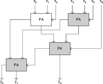
Figure 11.35 A 7-operand 1-bit adder.

Figure 11.36 Binary 5-operand ripple-carry adder.
An easy method for understanding the working of many arithmetic circuits is the dot notation. As an example, the function of a (7,3)-counter (namely, to reduce the sum of seven digits to three digits) is shown in Figure 11.37a, and that of the corresponding (7,3)-stored-carry encoder (namely, to substitute the sum of seven numbers by the sum of three numbers) in Figure 11.37b.
This type of notation facilitates the understanding of more complex counters. As an example, the function of a (5,5;4)-counter (Figure 11.38a) is to reduce the sum of five 2-digit numbers to four digits. So it is defined by the following relation:
![]()
By connecting in parallel n such (5,5;4)-counters (Figure 11.38b), a (5,2)-stored-carry-encoder is generated. Its function is to substitute the sum of five numbers by the sum of two numbers.
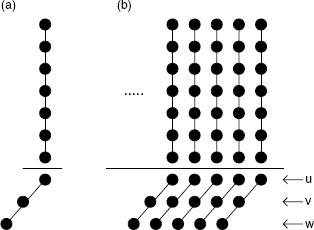
Figure 11.37 (a) A (7,3) counter and (b) a (7,3) stored-carry encoder.

Figure 11.38 (a) A (5,5;4) counter and (b) a (5,2) stored-carry encoder.
A (5,5;4)-counter, implemented with (3,2)-counters, is shown in Figure 11.39, and a (5,2)-stored-carry encoder in Figure 11.40.
According to Figures 11.39 and 11.40, the cost and computation time of the (5,2)-stored-carry encoder are equal to
![]()
The (5,2)-stored-carry encoder can be used for generating carry-save trees. For example, a 26-to-2 carry-save tree is shown in Figure 11.41. It expresses the sum of 26 numbers x(0), x(1), …, x(25), under the form y + z. With an additional 2-operand adder, a 26-operand adder is generated. Its cost and computation time are equal to

Figure 11.39 A (5,5;4) counter.
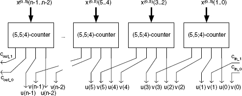
Figure 11.40 A (5,2) stored-carry encoder.
The (5,5;4)-counter is a particular case of the following type of computation resource:
Definition 11.4 A (pr − 1, pr − 2, …, p0; k)-counter is a (pr − 1 + pr − 2 + … + p0)-input k-output combinational circuit whose behavior is defined by the following equation:
![]()

Figure 11.41 A 26-to-2 carry-save tree.
(where p(j) stands for pj). The output vector y represents the number of units within the input vector x0, plus B times the number of units within the input vector x1, plus B2 times the number of units within the input vector x2, and so on.
Example 11.13 (Complete VHDL code available.) Generate the VHDL model of a binary 31-to-3 carry-save tree (Figure 11.34):
 entity seven_to_three is
 port (
   x_0, x_1, x_2, x_3, x_4, x_5, x_6: in std_logic;
   y_2, y_1, y_0: out std_logic
 );
 end seven_to_three;

 architecture circuit of seven_to_three is
   component full_adder…end component;
   signal a, b, c, d, e: std_logic;
 begin
   fa_1: full_adder port map(x_3, x_4, x_5, b, a);
   fa_2: full_adder port map(x_0, x_1, x_2, d, c);
   fa_3: full_adder port map(c, a, x_6, e, y_0);
   fa_4: full_adder port map(d, b, e, y_2, y_1);
 end circuit;

 entity stored_carry_encoder is
 port (
   x_0, x_1, x_2, x_3, x_4, x_5, x_6:
   in std_logic_vector(n-1 downto 0);
   u, v, w: out std_logic_vector(n-1 downto 0)
 );
 end stored_carry_encoder;

 architecture circuit of stored_carry_encoder is
   component seven_to_three…end component;
   signal v_n, w_n, w_nn: std_logic;
 begin
   v(0)<=‘0’; w(1)<=‘0’; w(0)<=‘0’;
   main_loop: for i in 0 to n-3 generate
     iterative_step: seven_to_three port map (x_0(i),x_1(i),
     x_2(i),x_3(i),x_4(i),x_5(i),x_6(i),
     w(i+2), v(i+1), u(i));
   end generate;
   second_last_step: seven_to_three port map
  (x_0(n-2),x_1(n-2),x_2(n-2),x_3(n-2),x_4(n-2),
   x_5(n-2),x_6(n-2), w_n, v(n-1), u(n-2));
   last_step: seven_to_three port map
   (x_0(n-1),x_1(n-1),x_2(n-1),x_3(n-1),x_4(n-1),
   x_5(n-1),x_6(n-1), w_nn, v_n, u(n-1));
  end circuit;

  entity carry_save_tree is
  port (
    x_0, x_1,…, x_30: in std_logic_vector(n-1 downto 0);
    y, z, w: out std_logic_vector(n-1 downto 0)
  );
  end carry_save_tree;

  architecture circuit of carry_save_tree is
    component stored_carry_encoder…end component;
    signal a1, a2,…, a12: std_logic_vector(n-1 downto 0);
    signal b1, b2, b3, b4, b5, b6: std_logic_vector(n-1 downto 0);
  begin
    encoder_1: stored_carry_encoder port map(x_2, x_3, x_4, x_5,
    x_6, x_7, x_8, a1, a2, a3);
    encoder_2: stored_carry_encoder port map(x_9, x_10, x_11,
    x_12, x_13, x_14, x_15, a4, a5, a6);
    encoder_3: stored_carry_encoder port map(x_16, x_17, x_18,
    x_19, x_2 0, x_21, x_2 2, a7, a8, a9);
    encoder_4: stored_carry_encoder port map(x_2 3, x_24, x_25,
    x_26, x_27, x_2 8, x_29, a10, a11, a12);
    encoder_5: stored_carry_encoder port map(x_1, a1, a2, a3, a4,
    a5, a6, b1, b2, b3);
    encoder_6: stored_carry_encoder port map(a7, a8, a9, a10,
    a11, a12, x_3 0,b4, b5, b6);
    encoder_7: stored_carry_encoder port map(x_0, b1, b2, b3, b4,
    b5, b6, y, z, w);
  end circuit;
11.1.13 Subtractors and Adder-Subtractors
Given two n-digit natural numbers x and y, and an input borrow b_in, the difference z=x − y − b_in could be a negative number. So, in the case of natural numbers, the subtractors must have a status output (a flag), indicating that the result of the subtraction is not a natural number. A first option consists in implementing Algorithm 4.17. The corresponding circuit—a ripple-carry subtractor—is made up of n full-subtractor (FS) cells (Figure 11.42) whose behavior is the following:
Another option is to use a simplified version of the Algorithm 4.21.
Algorithm 11.1 Natural Number Subtraction
for i in 0… n loop y′ (i): = B-1-y(i); end loop;
c_in:=1-b_in;
natural_addition(n, x, y′, c_in, z, c_out);
negative:=1-c_out;

Figure 11.42 Ripple-carry subtractor.
The advantage of the second method is that any type of adder can be used, so that all the adder implementations presented in the preceding sections can be considered. Furthermore, it's easy to design an adder/subtractor based on Algorithm 11.1 (Figure 11.43a):
if control = 0 the circuit computes the (n + 1)-digit number z = x + y + d_in, where z(n) = d_out;
if control = 1 and if x − y − d_in is nonnegative, the circuit computes the n-digit number z = x − y − d_in and the d_out output flag is put to 0; if x − y − d_in is negative, the d_out output flag is raised.
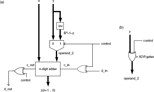
Figure 11.43 Adder-subtractor.
In the preceding circuit the combinational block inv is made up of n identical subcircuits that compute B − 1 − y(i) for every digit y(i) of y. If B = 2 then every subcircuit is an inverter. Furthermore, the n inverters and the multiplexer could be replaced by n XOR gates (Figure 11.43b).
Example 11.14 (Complete VHDL code available.) Generate the VHDL model of an adder-subtractor (Figure 11.43).
  entity example11_14 is
  port (
    x, y: in digit_vector(n-1 downto 0);
    control, d_in: in std_logic;
    z: out digit_vector(n-1 downto 0);
    d_out: out std_logic
  );
  end example11_14;
  architecture circuit of example11_14 is
    signal minus_y, operand_2: digit_vector(n-1 downto 0);
    signal carries: std_logic_vector(n downto 0);
  begin
    invert: for i in 0 to n-1 generate minus_y(i)<=B-1-y(i);
    end generate;
    with control select
    operand_2<=y when ‘0’, minus_y when others;
    carries(0)<=control xor d_in;
    adder: for i in 0 to n-1 generate
      iterative_step: z(i)<=(x(i)+operand_2(i)+
      conv_integer(carries(i))) mod B;
      carries(i+1)<=‘0’ when x(i)+operand_2(i)+
      conv_integer(carries(i))<B else ‘1’;
    end generate;
    d_out<=carries(n) xor control;
  end circuit;
11.1.14 Termination Detection
Self-timed circuits (Section 10.4) constitute an attractive option to build reliable and time-effective circuits. An example of their implementation has been seen in Chapter 10 (Example 10.6). In this section a slightly different approach is proposed: instead of computing the actual done condition a simpler condition is computed; nevertheless in most cases it will be equivalent to the done one ([BIO2003]).
For that purpose an n-bit adder is decomposed into n/s s-bit groups, and the propagation conditions p(i.s + s − 1:i.s) are computed as in the case of an s-bit carry-skip chain (Figure 11.6). Assume now that all the propagation conditions p(i.s + s − 1:i.s), i = 0,…, n/s − 1, are equal to 0. Then all the carries must have been generated or killed within the group or its predecessor. As a consequence, sum completion for the n-bit adder is guaranteed after a time delay less than
where Tadder(2.s) is the computation time of a partial adder made up of two successive groups.
The probability α of all propagation conditions p(i.s + s − 1:i.s) being equal to 0 is
Observe that if s is great enough, then
in such a way that if n/s << 2s, then α ≅ 1. Some particular values are given in Table 11.3.
Define the stat-done flag as follows:
![]()
An example of how to use the stat-done flag is shown in Figure 11.44. The circuit of Figure 11.44a is assumed to be part of a signal processing system. It is made up of an n-bit adder that generates the stat-done flag and an output register. The clock period must be greater than both Tcompletion (11.83) and the computation time of stat-done. The adder works as follows (Figure 11.44.b):
- if stat-done is equal to 1, the addition is performed within one clock cycle;
- if stat-done is equal to 0, a wait instruction is executed; the delay value is defined by the maximum computation time (a value that can be previously computed); according to Table 11.3 the value of s can be chosen in such a way that the probability of stat-done being equal to 0 is very small.
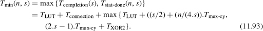
The minimum clock period is equal to
TABLE 11.3 Probability α of All p(i.s 1 s − 1:i.s) Being Equal to 0


Figure 11.44 Statistical approach.
where Tcompietjon(s) is the computation time of a partial adder made up of two successive groups, and Tstat-done(n, s) is the computation time of the stat-done flag.
The average computation time is equal to
Using (11.85),
For great values of n, the value of s can be chosen in such a way that
11.1.15 FPGA Implementation of the Termination Detection
The computation of the stat-done flag is performed as follows:
- Computation of p(s − 1: 0), p(2.s − 1: s),…, p(n.s − 1:(n − 1).s). An FPGA implementation is shown in Figure 11.23; the corresponding cost Cp and delay Tp are equal to (11.62)

- The computation of stat-done = not(p(s − 1:0) ∨ p(2.s − 1: s) ∨ … ∨ p(n.s − 1:(n − 1).s)) is performed with the circuit of Figure 11.45; the look-up tables compute

Figure 11.45 stat-done flag generation.

Its cost Cpb and computation time Tpb are equal to
The cost Cstat-done and computation time Tstat-done of the stat-done flag are equal to
The previous values (11.62), (11.90), and (11.91) are correct as long as both s/4 and n/(8.s) are smaller than the number of rows of the selected circuit matrix. Assume now that s/2 is also smaller than the number of rows. Then every s-bit group of the adder (Figure 11.25) can be placed within one column, so that Tcompletion, namely the computation time of a 2.s-digit adder, is equal to (see relation (11.59))
According to (11.86), (11.91), and (11.92), the minimum clock period Tclk of the system of Figure 11.44 is equal to
Example 11.15 Several adders have been implemented within a Spartan II FPGA. Tools and conditions are similar to the ones used in Section 11.1.10.3. The main results are summarized in Table 11.4.