9.4 PROGRAMMABLE LOGIC
Logic devices can be classified into two broad categories: fixed and programmable. Circuits in a fixed logic device are permanent: they perform one function or set of functions, and once manufactured, they cannot be changed, as traditional ASICs can. On the other hand, programmable logic devices (PLDs) are standard, off-the-shelf parts that can be modified at any time to perform any number of functions. A key benefit of using PLDs is that, during the design phase, designers can change the circuitry as often as they want until the design operates satisfactorily. PLDs are based on rewritable memory technology: to modify the design, the device only needs to be reprogrammed. Reusability is a further attractive feature of PLDs. Many types of programmable logic devices are currently available. The range of market products includes small devices capable of implementing a handful of logic equations up to huge FPGAs that can hold an entire processor core plus a number of peripherals. Besides this impressive diversity of sizes, numerous alternative architectures are offered to the designer. Within programmable logic devices, two major types deserve to be highlighted: the complex programmable logic device (CPLD) and field programmable gate array (FPGA). They are described below.
9.4.1 Programmable Logic Devices (PLDs)
At the low end of the spectrum stand the original programmable logic devices (PLDs). They were the first chips that could be used as hardware implementation of a flexible digital logic design. For instance, a couple of the 74xxx board parts could be removed and replaced by a single PLD. Other names also stand for this class of device: programmable logic array (PLA), programmable array of logic (PAL), and generic array logic (GAL). A PLD is made of a fully connected set of macrocells. These macrocells typically consist of some combinational logic (typically AND/OR gates and a flip-flop: Figure 9.15). A small Boolean equation can thus be built within each macrocell. This equation will convert the state of some binary inputs into a binary output and, if necessary, store that output in a flip-flop until the next clock edge. Obviously, the characteristics of the available logic gates and flip-flops are specific to each manufacturer and product family. But the general idea holds for any product. Hardware descriptions for these simple PLDs are generally either written in languages like ABEL or PALASM (the HDL equivalent of assembler) or drawn with the help of a schematic capture tool.

Figure 9.15 Typical PLD architecture.
As chip densities increased, PLD manufacturers naturally developed their products toward larger parts, called complex programmable logic devices (CPLDs). In a certain respect, CPLDs can be described as several PLDs (plus some programmable interconnection) in a single chip. The larger size of a CPLD allows implementing either more logic equations or more complicated designs.
Figure 9.16 contains a block diagram of a typical CPLD: within each logic block stands the equivalent of one PLD. Because CPLDs can hold larger designs than PLDs, their potential uses are quite wide-ranging. Sometimes they are used for simple applications, like address decoding, but more often they contain high-performance control-logic or complex finite state machines. At the high-end (in terms of numbers of gates), there is some overlapping with FPGAs in potential applications. Traditionally, CPLDs have been preferred over FPGAs whenever high-performance logic is required. Because of its less flexible internal architecture, delays through a CPLD are more predictable and usually shorter.

Figure 9.16 Internal structure of a theoretical CPLD.
9.4.2 Field Programmable Gate Array (FPGA)
Field programmable gate arrays (FPGAs) can be used to implement just about any hardware design. One common use of the FPGA is the prototyping of a piece of hardware that will eventually be implemented later into an ASIC. Nevertheless, FPGAs have been increasingly used as the final product platforms. Their use depends, for a given project, on the relative weights of desired performances, development, and production costs. See Section 9.1.2.2.
9.4.2.1 Why FPGA? A Short Historical Survey
By the early 1980s, most of the typical logic circuit systems were implemented within a small variety of standard large scale integrated (LSI) circuits: microprocessors, bus-I/O controllers, system timers, and so on. Nevertheless, every system still had the need for random “glue logic” to connect the large ICs, for example, generate global control signals and data formatting (serial to parallel, multiplexing, etc.). Custom ICs were often designed to replace the large amount of glue logic and consequently reduce system complexity and manufacturing cost, as well as improve performances. However, custom ICs are expensive to develop, while generating time-to-market (TTM) delays because of the prohibitive design time. Therefore the custom IC approach was only viable for products with very high volume (lowering the NRE cost impact), and not TTM sensitive. Coping with this problem, Xilinx™ (a startup company) introduced, in 1984,2 the FPGA technology as an alternative to custom ICs for implementing glue logic. Thanks to computer-aided design (CAD) tools, FPGA circuits can be implemented in a relatively short amount of time: no physical layout process, no mask making, no IC manufacturing, lower NRE costs, and short TTM.
9.4.2.2 Basic FPGA Concepts
The basic FPGA architecture consists of a two-dimensional array of logic blocks and flip-flops with means for the user to configure (i) the function of each logic blocks, (ii) the inputs/outputs, and (iii) the interconnection between blocks (Figure 9.17). Families of FPGAs differ from each other by the physical means for implementing user programmability, arrangement of interconnection wires, and basic functionality of the logic blocks.
Programming Methods There are three main types of programmability:
- SRAM Based (e.g., Xilinx™, Altera™): FPGA connections are achieved using pass-transistors, transmission gates, or multiplexers that are controlled by SRAM cells (Figure 9.18). This technology allows fast in-circuit reconfiguration. The major disadvantages are the size of the chip, required by the RAM technology, and the needs of some external source (usually external nonvolatile memory chips) to load the chip configuration. The FPGA can be programmed an unlimited number of times.
Figure 9.17 Basic architecture of FPGA: two-dimensional array of programmable logic cells, interconnections, and input/ouput.
- Antifuse Technology (e.g., Actel™, Quicklogic™): an antifuse remains in a high-impedance state until it is programmed into a low-impedance or “fused” state (Figure 9.18). This technology can be used only once on one-time programmable (OTP) devices; it is less expensive than the RAM technology.
- EPROM/EEPROM Technology (various PLDs): this method is the same as that used in EPROM/EEPROM memories. The configuration is stored within the device, that is, without external memory. Generally, in-circuit reprogramming is not possible.

Look-Up Tables The way logic functions are implemented in a FPGA is another key feature. Logic blocks that carry out logical functions are look-up tables (LUTs), implemented as memory, or multiplexer and memory. Figure 9.19 shows these alternatives, together with an example of memory contents for some basic operations. A 2n × 1 ROM can implement any n-bit function. Typical sizes for n are 2, 3, 4, or 5.
In Figure 9.19a, an n-bit LUT is implemented as a 2n × 1 memory; the input address selects one of 2n memory locations. The memory locations (latches) are normally loaded with values from the user's configuration bit-stream. In Figure 9.19b, the multiplexer control inputs are the LUT inputs. The result is a general-purpose “logic gate.” An n-LUT can implement any n-bit function.

Figure 9.18 Programming methods: (a) SRAM connection and (b) antifuse.

Figure 9.19 Look-up table implemented as (a) memory or (b) multiplexer and memory. (c) Memory contents example for different logic functions.
An n-LUT is a direct implementation of a function truth table. Each latch location holds the value of the function corresponding to one input combination. An example of a 4-LUT is shown in Figure 9.20.
FPGA Logic Block A simplified FPGA logic block can be designed with a LUT, typically a 4-input LUT, implementing a combinational logic function, and a register that optionally stores the output of the logic generator (Figure 9.21).
9.4.3 Xilinx™ Specifics
This section is devoted to the description of the Xilinx Virtex family ([XIL2001]) and, in particular, the Spartan II ([XIL2004c]), a low cost version of Virtex. The Virtex II ([XIL2004a]) device family is a more recent and powerful architecture, sharing most of the capabilities and basic concepts of Virtex. Spartan III ([XIL2004b]) is the low-cost version of Virtex II. Finally, Virtex II-Pro features additional hardwired Power-PC processors. For simplicity, minor details are omitted in the following.

Figure 9.20 4-LUT implementation and the truth-table contents.

Figure 9.21 A basic FPGA logic block.
All Xilinx FPGAs contain the same basic resources (Figure 9.22):
- Configurable logic blocks (CLBs), containing combinational logic and register resources.
- Input/output blocks (IOBs), interface between the FPGA and the outside world.
- Programmable interconnections (PIs).
- RAM blocks.
- Other resources: three-state buffers, global clock buffers, boundary scan logic, and so on.
Furthermore, Virtex II and Spartan III devices contain resources such as dedicated multipliers and a digital clock manager (DCM). The Virtex II-Pro also includes embedded Power-PC processors and full-duplex high-speed serial transceivers.

Figure 9.22 Example of distribution of CLBs, IOBs, PIs, RAM blocks, and multipliers in Virtex II.
9.4.3.1 Configurable Logic Blocks (CLBs)
The basic building block of Xilinx CLBs is the slice. Virtex and Spartan II hold two slices in one CLB, while Virtex II and Spartan III hold four slices per CLB. Each slice contains two 4-input function generators (F/G), carry logic, and two storage elements. Each function generator output drives both the CLB output and the D-input of a flip-flop. Figure 9.23 shows a detailed view of a single Virtex slice. Besides the four basic function generators, the Virtex/Spartan II CLB contains logic that combines function generators to provide functions of five or six inputs. The look-up tables and storage elements of the CLB have the following characteristics:
- Look-Up Tables (LUTs): Xilinx function generators are implemented as 4-input look-up tables. Beyond operating as a function generator, each LUT can be programmed as a (16 × 1)-bit synchronous RAM. Furthermore, the two LUTs can be combined within a slice to create a (16 × 2)-bit or (32 × 1)-bit synchronous RAM, or a (16 × 1)-bit dual-port synchronous RAM. Finally, the LUT can also provide a 16-bit shift register, ideal for capturing high-speed data.
- Storage Elements: The storage elements in a slice can be configured either as edge-triggered D-type flip-flops or as level-sensitive latches. The D-inputs can be driven either by the function generators within the slice or directly from the slice inputs, bypassing the function generators. As well as clock and clock enable signals, each slice has synchronous set and reset signals.
9.4.3.2 Input/Output Blocks (IOBs)
The Xilinx IOB includes inputs and outputs that support a wide variety of I/O signaling standards. The IOB storage elements act either as D-type flip-flops or as latches. For each flip-flop, the set/reset (SR) signals can be independently configured as synchronous set, synchronous reset, asynchronous preset, or asynchronous clear. Pull-up and pull-down resistors and an optional weak-keeper circuit can be attached to each pad. IOBs are programmable and can be categorized as follows:
- Input Path: A buffer in the IOB input path is routing the input signals either directly to internal logic or through an optional input flip-flop.
- Output Path: The output path includes a 3-state output buffer that drives the output signal onto the pad. The output signal can be routed to the buffer directly from the internal logic or through an optional IOB output flip-flop. The 3-state control of the output can also be routed directly from the internal logic or through a flip-flop that provides synchronous enable and disable signals.
- Bidirectional Block: This can be any combination of input and output configurations.
9.4.3.3 RAM Blocks
Xilinx FPGA incorporates several large RAM memories (block select RAM). These memory blocks are organized in columns along the chip. The number of blocks, ranging from 8 up to more than 100, depends on the device size and family. In Virtex/Spartan II, each block is a fully synchronous dual-ported 4096-bit RAM, with independent control signals for each port. The data width of the two ports can be configured independently. In Virtex II/ Spartan III, each block provides 18-kbit storage.

Figure 9.23 Simplified Virtex slice and IOB.
9.4.3.4 Programmable Routing
Adjacent to each CLB stands a general routing matrix (GRM). The GRM is a switch matrix through which resources are connected (Figure 9.24); the GRM is also the means by which the CLB gains access to the general-purpose routing. Horizontal and vertical routing resources for each row or column include:
- Long Lines: bidirectional wires that distribute signals across the device. Vertical and horizontal long lines span the full height and width of the device.
- Hex Lines route signals to every third or sixth block away in all four directions.
- Double Lines: route signals to every first or second block away in all four directions.
- Direct Lines: route signals to neighboring blocks—vertically, horizontally, and diagonally.
- Fast Lines: internal CLB local interconnections from LUT outputs to LUT inputs.
The routing performance factor of internal signals is the longest delay path that limits the speed of any worst-case design. Consequently, the Xilinx routing architecture and its place-and-route software were defined in a single optimization process.
Xilinx devices provide high-speed, low-skew clock distribution. Virtex provides four primary global nets that drive any clock pin; instead, Virtex II has 16 global clock lines—eight per quadrant.
9.4.3.5 Arithmetic Resources in Xilinx FPGAs
Modern FPGAs have special circuitry to speed-up arithmetic operations. Therefore adders, counters, multipliers, and other common operators work much faster than the same operations built from LUTs and normal routing only.
Dedicated carry logic provides fast arithmetic carry capability for high-speed arithmetic functions. There is one carry chain per slice; the carry chain height is 2 bits per slice. The arithmetic logic includes one XOR gate that allows a 1-bit full adder to be implemented within the available LUT (see Section 11.1.10). In addition, a dedicated AND gate improves the efficiency of multiplier implementations (see Section 12.1.7).
The dedicated carry path can also be used to cascade function generators for implementing wide logic functions.
9.4.4 FPGA Generic Design Flow
The FPGA design flow has several points in common with the semicustom ASIC design flow. Figure 9.25 presents a simplified FPGA design flow. The successive process phases (blocks) of Figure 9.25 are described as follows:
- Design Entry: creation of design files using schematic editor or hardware description language (Verilog, VHDL, Abel).
- Design Synthesis: a process that starts from a high level of logic abstraction (typically Verilog or VHDL) and automatically creates a lower level of logic abstraction using a library of primitives.
- Partition (or Mapping): a process assigning to each logic element a specific physical element that actually implements the logic function in a configurable device.
- Place: maps logic into specific locations in the target FPGA chip.
- Route: connections of the mapped logic.
- Program Generation: a bit-stream file is generated to program the device.
- Device Programming: downloading the bit-stream to the FPGA.
- Design Verification: simulation is used to check functionalities. The simulation can be done at different levels. The functional or behavioral simulation does not take into account component or interconnection delays. The timing simulation uses back-annotated delay information extracted from the circuit. Other reports are generated to verify other implementation results, such as maximum frequency and delay and resource utilization.

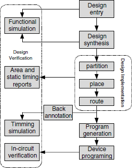
The partition (or mapping), place, and route processes are commonly referred to as design implementation.