
12.2 INTEGERS
12.2.1 B's Complement Multipliers
A straightforward implementation of Algorithm 5.7 (Section 5.3.1.1: mod Bn+m B's complement multiplication) consists of extending the representation of X and Y to n + m digits and computing the n + m less significant digits of R(Z) = R(X).R(Y). For that purpose any natural-number multiplier can be used. As an example, assume that a carry-save multiplier is used (Figure 12.5). The adder, ripple-carry, or whatever is no longer necessary as the n + m most significant digits must be truncated. So the array is limited to the rightmost n + m columns of the array represented in Figure 12.5. The cost and computation time of the obtained array are
![]()
where C2 and T2 are the cost and propagation time of the cell of Figure 12.3.
If m = n, then C(n) = n.(2.n + 1).C2, and T(n, m) = 2.n.T2. The computation time is the same as in the case of the natural numbers (12.3) but the cost is almost twice the cost CCSM = n.(n + 1).C2 given by formula (12.4).
Another option is to implement Algorithm 5.8. A circuit similar to the ripple-carry multiplier of Figure 12.4 can be used. Every cell of the last row (Figure 12.3 with i = n − 1) must be replaced by a different one whose behavior is defined by the following rules:
The cost and the computation time are (practically) the same as in the case of a ripple-carry multiplier for natural numbers.
A third option is a straightforward implementation of relation (5.10) of Section 5.2.1.3:
![]()
The block diagram, shown in Figure 12.23, has to be interpreted in the following manner.
- The product X0.Y0 is an (n + m − 2)-bit positive number with sign extension.

Figure 12.23 Postcorrection B's complement multiplication scheme.
 stand for sign digits
  (see Chapter 5, Section 5.2.1.3).
- If
 correction
  vanishes.
 - Whenever
 is nonzero, the correcting term is built up by changing the sign of (0, Y0) left-shifted by (n − 1) positions with sign extension (resp. (0, X0) left-shifted by (m − 1) positions with sign extension).
 - Whenever both
 and
and  are nonzero, a left-shifted 1 ((n + m − 2) positions plus sign extension) is added.
The above-mentioned operations are a lot simpler in 2's complement; moreover thanks to the simplifications suggested by Baugh and Wooley ([BAU1973]), the circuit of Figure 12.4 or 12.5 can be used with the following modifications:
- In the basic cell (Figure 12.3b), the and products
 and
and  have to be complemented, which is readily achieved by replacing the AND by a NAND gate in the corresponding cells. Observe that xn−1.ym−1 remains unchanged.
 - A bit 1 has to be added at levels m − 1 and n − 1 (a single 1 at level n if m = n).
- A bit 1 (sign) has to be added at level m + n − 1 (at level 2n − 1 if m = n).
The cost and the computation time are (practically) the same as in the case of the corresponding multiplier array for natural numbers (Figure 12.4 or 12.5).
12.2.2 Booth Multipliers
12.2.2.1 Booth-1 Multiplier
One first considers a Booth-1 representation for the n-bit binary 2's complement number X. In this case r = 1 means k = n and B = 2. According to formula (5.12) of Chapter 5, Booth-1 coding is defined as
![]()
The circuit corresponding to Algorithm 5.10 (Section 5.2.3.1) is an iterative one made up of n steps (Figure 12.24a). Step number i generates the value of ![]() as a function of
as a function of ![]() and xi, according to the following recurrence formulas:
and xi, according to the following recurrence formulas:
The final result is pnzn−1 … z0. Observe that all pi are m-bit numbers and that the circuit corresponding to equation (12.8) behaves like an adder/subtractor controlled by xi−1 and xi; in particular, the Boolean function ![]() may be used to control the sign of Y (negative if S = 1) while the function
may be used to control the sign of Y (negative if S = 1) while the function ![]() controls if ± Y is added (P = 1) or not (P = 0). Figure 12.24b depicts a possible implementation of the m-bit adder/subtractor assuming both pi and Y expressed in 2's complement.
controls if ± Y is added (P = 1) or not (P = 0). Figure 12.24b depicts a possible implementation of the m-bit adder/subtractor assuming both pi and Y expressed in 2's complement.
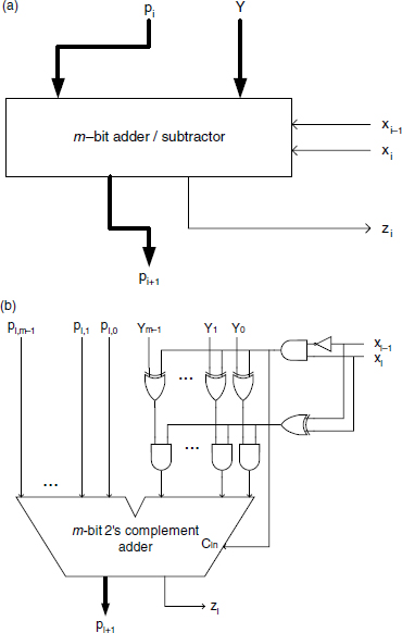
Figure 12.24 (a) Booth-1 multiplier step. (b) Booth-1 multiplier step implementation.
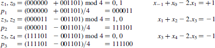
Example 12.10 Let X = 101011 and Y = 01101 (n = 6, m = 5), both given in 2's complement representation The circuit of Figure 12.24b (p0 is assumed 0) will compute recursively:

12.2.2.2 Booth-2 Multiplier
Let us focus now on the Booth-2 representation. In this case, r = 2, k = n/2, and B = 2. According to formula (5.12) of Chapter 5, Booth-2 coding is defined as
![]()
thus ![]() .
.
The circuit corresponding to Algorithm 5.10 (Section 5.2.3.1) is now made up of k = n/2 iterative steps (Figure 12.25a). Step number i generates the value of ![]() as a function of
as a function of ![]() and X2.i+1:
and X2.i+1:
Two bit results z2.i+1 and z2.i are generated at each step. The final result is ![]() Observe that all pi are still m-bit numbers but the circuit corresponding to equation (12.9) must now be able to compute pi + Y, pi − Y, pi + 2.Y, and Pi − 2.Y. The corresponding behavior is that of an adder/subtractor/left-shifter controlled by x2.i−1, x2.i and x2.i+1, as shown in Figure 12.25a. The control functions may be expressed as
Observe that all pi are still m-bit numbers but the circuit corresponding to equation (12.9) must now be able to compute pi + Y, pi − Y, pi + 2.Y, and Pi − 2.Y. The corresponding behavior is that of an adder/subtractor/left-shifter controlled by x2.i−1, x2.i and x2.i+1, as shown in Figure 12.25a. The control functions may be expressed as

S controls the sign (S = 1 for negative), P = 1 enables the sum (P = 0 for adding zero), and SL controls a one-position left-shift of Y (SL = 1 for shift). Shift registers are common in most microprocessors, but for high-speed shift, more specific circuits may be designed (Figure 12.25b). A possible combinational implementation of the control circuit is presented in Figure 12.25c. In FPGA implementations, high-speed look-up tables are used to implement those control functions. Figure 12.25d presents a detailed combinational implementation of the Booth-2 multiplier step.


Figure 12.25 (a) Booth-2 multiplier step. (b) A 1-bit left-shifter. (c) Control circuit for Booth-2 multiplier. (d) Booth-2 multiplier step implementation.
The most prominent feature of the Booth-2 algorithm with respect to Booth-1 rests on the number of steps: n/2 instead of n. Matching up Figures 12.24a–12.24b to Figures 12.25a–12.25d highlights the fact that the hardware complexity is quite similar for both implementations. Booth-2 needs additional resources: a shifter, an (m + 1)-bit adder instead of an m-bit adder, and a slightly more sophisticated control circuit.
Example 12.11 Let X = 10101101 and Y = 01101 (n = 8, m = 5), both given in 2's complement representation. The circuit of Figures 12.25a–12.25d (p0 is assumed 0) will compute recursively:
Note: For clarity, all successive values of pi, but the last one, have been extended to 6 bits.
Comment 12.3 Higher-level Booth-r multipliers (r > 2) appear more intricate because of the complexity of the ![]() . For example, Booth-3 coding would generate
. For example, Booth-3 coding would generate ![]() digits in the range [− 4, +4]. Besides adding, shifting and sign change, implementation of multiplication by 3 is also needed. A possible approach might consist of a previous computation of the suitable multiples of Y, to be then stored in a fast-access memory.
digits in the range [− 4, +4]. Besides adding, shifting and sign change, implementation of multiplication by 3 is also needed. A possible approach might consist of a previous computation of the suitable multiples of Y, to be then stored in a fast-access memory.
Example 12.12 (Complete VHDL source code available.) Generate a generic n-bit by m-bit Booth-1 multiplier for signed operands. The basic multiplier cell (Figure 12.24) is:
entity booth_1_cell is
Port (
  P: in std_logic_vector(M-1 downto 0);
  Y: in std_logic_vector(M-1 downto 0);
  x_i: in std_logic_vector(1 downto 0);
  S: out std_logic_vector(M downto 0)
  );
end booth_1_cell;

architecture behavioral of booth_1_cell is
begin
  the_mux: process(x_i,P, Y)
  begin
    case x_i is
      when “00”=>S<=(P(M-1) & P);
      when “01”=>S<=(P(M-1) & P)+(Y(M-1) & Y);
      when “10”=>S<=(P(M-1) & P)-(Y(M - 1) & Y);
      when “11”=>S<=(P(M-1) & P);
      when others=>NULL;
    end case;
  end process;
end behavioral;
The complete Booth-1 multiplier is:
entity booth_1 is
port (
  X: in std_logic_vector (N-1 downto 0);
  Y: in std_logic_vector (M-1 downto 0);
  P: out std_logic_vector (N+M-1 downto 0)
  );
end booth_1;

architecture simple_arch of booth_1 is
  type connect is array (0 to N) of std_logic_vector (M downto 0);
  signal wires: connect;
  signal eX: std_logic_vector (N downto 0);
begin
  eX(N downto 1)<=X; eX(0)<=‘0’;
  wires(0)<=(others=>‘0’);
  iterac: for i in 0 to N-1 generate
    mult: booth_1_cell port map (wires(i)(M downto 1), Y,
     eX(i+1 downto i), wires(i+1));
    p(i)<=wires(i+1)(0);
end generate;
P(M+N-1 downto N)<=wires(N)(M downto 1);
end simple_arch;
Example 12.13 (Complete VHDL source code available.) Generate a generic n-bit by m-bit Booth-2 multiplier for signed operands. The basic multiplier cell (Figure 12.25) is:
entity booth_2_cell is
Port (
  P: in std_logic_vector(M-1 downto 0);
  Y: in std_logic_vector(M-1 downto 0);
  X_i: in std_logic_vector(2 downto 0);
  Z: out std_logic_vector(1 downto 0);
  P_n: out std_logic_vector(M-1 downto 0)
  );
end booth_2_cell;

architecture behavioral of booth_2_cell is
signal long_P, long_Y, long_Y_2: std_logic_vector(M+1 downto
0);
signal S: std_logic_vector(M+1 downto 0);
begin
  long_P<=P(M-1) & P(M - 1) & P;
  long_Y<=Y(M - 1) & Y(M - 1) & Y;
  long_Y_2<=Y(M - 1) & Y & ‘0’;
  the_mux: process(x_i, long_P, long_Y, long_Y_2)
  begin
    case x_i is
      when “000”=>S<=long_P;
      when “001”=>S<=long_P+ long_Y;
      when “010”=>S<=long_P+ long_Y;
      when “011”=>S<=long_P+long_Y_2;
      when “100”=>S<=long_P-long_Y_2;
      when “101”=>S<=long_P-long_Y;
      when “110”=>S<=long_P-long_Y;
      when “111”=>S<=long_P;
     end case;
   end process;
   P_n<=S(M+1 downto 2); Z<=S(1 downto 0);
 end behavioral;
The complete Booth-2 multiplier is:
entity booth_2 is
port (
  X: in std_logic_vector (N-1 downto 0);
  Y: in std_logic_vector (M-1 downto 0);
  P: out std_logic_vector (N+M-1 downto 0)
  );
end booth_2;

architecture simple_arch of booth_2 is
type con is array (0 to N/2+1) of std_logic_vector (M-1 downto
0);
Signal wires: con
Signal eX: std_logic_vector (N+1 downto 0);
begin
  eX<=X(N-1) & X & ‘0’;
  wires(0)<=(others=>‘0’);
  iter: for i in 0 to (N+1)/2-1 generate
    mult: booth_2_cell port map (wires(i), Y,
     eX(2*i+2 downto 2*i), p(2*i+1 downto 2*i),wires(i+1));
  end generate;
  p(M+N-1 downto N+(N mod 2))<=
              wires((N+1)/2)(M-(N mod 2)-1 downto 0);
end simple_arch;
12.2.2.3 Signed-Digit Multiplier
Another type of multiplier can be deduced from Algorithm 5.12, in Section 5.2.3.2. It consists of a multiplier array processing Booth-coded signed digits. It is made up of an n/r by m/r array of signed-digit cells. The concept is introduced revisiting the example treated in Chapter 5: the 12-bit by 12-bit multiplier (m = n = 12) with Booth-3 (r = 3) digit coding. The general structure is shown in Figure 5.7. Assuming that the operands X and Y are initially given by their 2's complement representations, the method involves a preliminary coding according to formula (5.12) (see Algorithm 5.13: Booth_encode) and a final decoding process (Algorithm 5.14: Booth_decode). The Booth encoder and Booth decoder cells (r = 3) are shown in Figures 12.26 and 12.27, respectively. In this case, the bidimensional array uses cells computing functions G(a, b, c, d) and H(a, b, c, d) such that a.b + c + d = G.23+ H; a, b, c and d being elements of the set E = {− 4, −3,…, + 3, + 4}. If 2's complement codification is selected for the elements of E, the Booth encoding of X (resp. Y) can be achieved with the circuit of Figure 12.26. The input-output relation is given by

Figure 12.26 Booth-3 encoder cell.
According to formula (5.14), for r = 3, cell outputs G and H are in the range [− 4, +3]; actually as a, b, c, and d belong to the set E, the number (G, H) is in the following range:
![]()
In the same way, the adding array (Figure 5.7) produces signed digits in the range [−4, +3].
Figure 12.27 Booth-3 decoder cell.
A first option for the decoding of the multiplier output Z is an iterative circuit made up of (m + n)/3 steps (Algorithm 5.14a). Step number i generates the value of ![]() as a function of A(i) = aiz3.i−1 … z0 and Z(i):
as a function of A(i) = aiz3.i−1 … z0 and Z(i):
Algorithm 5.14b of Chapter 5 provides an alternative decoding circuit as described in Figure 12.28. Step i computes r new bits of the aimed 2's complement expression of Z(i), as a function of a carry (from the preceding step) and the r corresponding bits (signed digit zi) of the signed-digit expression of Z(i). This function actually subtracts modulo 2r from ![]() (zi, with its sign bit turned positive), the carry generated at the preceding step; the carry ci+1 is also generated. This carry ci+1 is the result of the potential positive adjustment of the first bit of (
(zi, with its sign bit turned positive), the carry generated at the preceding step; the carry ci+1 is also generated. This carry ci+1 is the result of the potential positive adjustment of the first bit of (![]() − ci). The circuit of Figure 12.28 is the materialization of the Boolean functions implementing the bitwise subtraction modulo-8:
− ci). The circuit of Figure 12.28 is the materialization of the Boolean functions implementing the bitwise subtraction modulo-8:
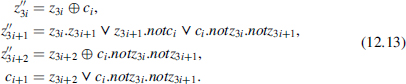
Figure 12.29 displays the generalized Booth-r decoder cell based on the same principle. The proposed cell may obviously be used sequentially or integrated in a full combinational iterative circuit.
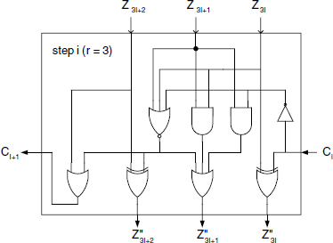
Figure 12.28 Booth-3 signed-digit decoder cell.
Figure 12.29 Booth-r signed-digit decoder cell.
Example 12.14 (Complete VHDL source code available.) Generate a generic n-bit by m-bit Booth-3 multiplier for signed operands. The basic multiplier cell (Figure 12.27) is:
entity booth_3_cell is
Port (
  P: in std_logic_vector(M-1 downto 0);
  Y: in std_logic_vector(M-1 downto 0);
  x_i: in std_logic_vector(3 downto 0);
  Z: out std_logic_vector(2 downto 0);
  P_n: out std_logic_vector(M-1 downto 0)
  );
end booth_3_cell;

architecture behavioral of booth_3_cell is
  signal s,l_P,l_Y,l_Y2,l_Y3,l_Y4: std_logic_vector(M+2 downto
  0);
begin
  l_P<=P(M-1) & P(M-1) & P(M-1) & P;
  l_Y<=Y(M-1)&Y(M-1)&Y(M-1)&Y; l_Y2<=Y(M-1)&Y(M-1)&Y&‘0’;
  l_Y3<=l_Y+ l_Y_2; l_Y4<=Y(M-1) & Y & “00”;
  the_mux: process(x_i,l_P, l_Y, l_Y2, l_Y3, l_Y4)
  begin
    case x_i is
      when “0000”|“1111”=>s<=l_P;
      when “0001”|“0010”=>s<=l_P+l_Y;
      when “0011”|“0100”=>s<=l_P+l_Y2;
      when “0101”|“0110”=>s<=l_P+l_Y3;
      when “0111”     =>s<=l_P+l_Y4;
      when “1000”     =>s<=l_P-l_Y4;
      when “1001”|“1010”=>s<=l_P-l_Y3;
      when “1011”|“1100”=>s<=l_P-l_Y2;
      when “1101”|“1110”=>s<=l_P-l_Y;
        end case;
      end process;
      P_n<=s(M+2 downto 3); Z<=s(2 downto 0);
end behavioral;
The complete Booth-3 multiplier is:
entity booth_3 is
port (
  X: in std_logic_vector (N-1 downto 0);
  Y: in std_logic_vector (M-1 downto 0);
  P: out std_logic_vector (N+M-1 downto 0)
  );
end booth_3;

architecture simple_arch of booth_3 is
  type connections is array (0 to (N+2)/3+1) of std_logic_vector
  (M−1 downto 0); signal wires: connections;
  signal eX: std_logic_vector (N+2 downto 0);
  constant bitsC: integer:=(3-(N mod 3)) mod 3;
begin
  eX<=X(N-1) & X(N-1) & X & ‘0’; wires(0)<=(others => ‘0’);
  iter: for i in 0 to (N+2)/3-1 generate
    mult: booth_3_cell port map (wires(i), Y,
          eX(3*i+3 downto 3*i),p(3*i+2 downto 3*i),wires(i+1));
    end generate;
  P(M+N-1 downto N+bitsC)<=wires((N+2)/3)(M-bitsC-1 downto 0);
end simple_arch;
Comment 12.4 The Per Gelosia adding technique can be applied. As an example, if m = n = 12 and r = 3, X and Y are represented with 4 digits belonging to E = {− 4, − 3,…,4}. The product of two digits belongs to the interval [−16, 16] and can be represented with two 3-bit 2's complement digits, thus within the range [(−4, −4), (3, 3)] in decimal [−36, 27]; as before, the digits of pij are constrained to belong to the range [−4, 3], which is sufficient to represent 2-digit numbers in the required range. A possible structure for the adding stage of the multiplier is described in what follows.
All the products pij = xi.yj are computed; xi and yj can be encoded with 4 bits (binary Booth encoding within E), while the 2-digit number pij needs 6 bits only; this corresponds to a cell with 8 inputs and 6 outputs. Moreover, it is possible to design an 8-input cell performing the coding together with the product as 6 Boolean functions of 8 variables: each 4-bit Booth-coded input is replaced by the 3 bits from the corresponding slice plus the 1 bit, from the next rightmost slice, involved in the Booth-coding operation. Standard minimization techniques can be used to provide a three-level NAND-gate circuit ([DAV1977]); alternatively, ROM (LUT) or PLA can be used.
The weighted sum of all pij can be performed according to the computation scheme of Figure 12.19, where each dot stands for a 3-bit 2's complement number; the sum of seven (or less) elements of {−4, − 3, …,3} belongs to the interval [− 28, 21] and can be represented by two digits within [(−3, −4), (3, −3)]. So, (7, 2), (5, 2), and (3, 2) counters can be synthesized to handle the overall sum. The scheme of Figure 12.20 is applicable but counters are now signed-digit counters; therefore, the design is somewhat different but with complexity comparable to that of base-8 counters. A (7, 2) signed-digit counter made up of signed-digit adders (Figure 12.30a) is presented in Figure 12.30b. Another alternative for the reducing stage is a carry-save array made up of signed-digit full adders. The signed digit full adder (SDFA: Figure 12.31) is similar to the adder of Figure 12.30a but is somewhat simpler in the sense that only 2-bit carries within {−1,0,1} are generated; this reduces the cell complexity to 8-input/5-output, instead of 9-input/6-output.
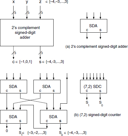
Figure 12.30 Signed-digit counter.

Figure 12.31 Signed-digit full adder.
In the same way that Booth encoding can be skipped, thanks to a special design of the multiplying cells, the output adders (SDOFA: Figure 12.32) from the final adding stage (e.g., ripple-carry adder) can be designed to cope with the Booth decoding process too. Actually, each adder of the chain has to add, with carry, signed digits in the range [− 4,3]. In order to avoid negative digits as a result (except for the last carry out), the adder cell is redesigned to generate a 3-bit positive digit sum S and a signed carry-out C in the range [− 2,1] accepting a carry-in in the same range [−2,1]. It is straightforward to note that the result of the above-mentioned sum remains in the (decimal) range [−10, 7] and can be expressed in a unique way in the form

Figure 12.32 Signed-digit output full adder.
where Ci, and Sj are the binary components of the signed carry-out C and the (positive) sum S, respectively. The inputs of the corresponding signed-digit output full adder (SDOFA) cell are similar to those of the SDFA of Figure 12.31 but the 3-bit output is now a positive 3-bit number while the carry-in and the carry-out are 2-bit signed digits in the range [−2,1]. The functions to be implemented are thus accordingly different. The last generated carry holds the bit-sign of the result.
12.2.3 FPGA Implementation of the Booth-1 Multiplier
An FPGA implementation of the circuit of Figure 12.24a is shown in Figure 12.33. The LUT functions are the following ones:

Figure 12.33 FPGA implementation of a Booth-1 multiplier step.

Figure 12.34 FPGA implementation of a Booth-1 multiplier.
if xi−1 = 1 and xi, = 0 then LUT_0 generates 0 and the other ones generate Yj xor Pj (addition);
if xi−1 = 0 and xi, = 1 then LUT_0 generates 1 and the other ones generate not(Yj) xor Pj (subtraction);
if xi−1 = xi, then LUT_0 generates 0 and the other ones generate Pj, so that cj+1 = not(Pj).Pj + Pj.Cj = 0 (c0 = 0) and Pj−1(i + 1) = 0 xor Pj(i) = Pj(i).
The general structure of the whole circuit (without LUT_0), along with one of the critical paths, is shown in Figure 12.34. The cost is equal to
![]()
and the computation time to
![]()
Observe that if m is not much greater than n then
![]()
so that the computation time is similar to that of a carry-save array.