
15.1 OPERATIONS IN Zm
15.1.1 Adders and Subtractors
The structure of a base-B modulo m adder is shown in Figure 15.1. It is based on Algorithm 8.2. Its cost is equal to

If every adder is a ripple-carry adder made up of full-adder cells, then its computation time is equal to
The structure of a modulo m subtractor is shown in Figure 15.2. It is based on Algorithm 8.4. Its cost and computation time are practically the same as in the case of the modulo m adder.
If every n-digit adder is a ripple-carry adder made up of full-adder cells, then its computation time is equal to
Example 15.1 (Complete VHDL source code available.) Generate VHDL models of binary (B = 2) modulo m adders and subtractors:
entity mod_adder is
port (
  x, y: in std_logic_vector(n-1 downto 0);
  z: out std_logic_vector(n-1 downto 0)
);
end mod_adder;

architecture circuit of mod_adder is
  signal z1, z2: std_logic_vector(n-1 downto 0);
  signal c1, c2: std_logic;
  signal long_x, long_y, long_result1, long_z1, minus_m,
  long_result2: std_logic_vector(n downto 0);
begin
  long_x<=‘0’&x; long_y<=‘0’&y;
  long_result1<=long_x+long_y;
  c1<=long_result1(n);
  z1<=long_result1(n-1 downto 0);
  long_z1<=‘0’&z1;
  minus_m<=conv_std_logic_vector((2**n)-m, n+1);
  long_result2<=long_z1+minus_m;
  c2<=long_result2(n);
  z2<=long_result2(n-1 downto 0);
  z<=z1 when (c1 or c2)=‘0’ else z2;
end circuit;

entity mod_subtractor is
port (
  x, y: in std_logic_vector(n-1 downto 0);
  z: out std_logic_vector(n-1 downto 0)
);
end mod_subtractor;

architecture circuit of mod_subtractor is
  signal z1, z2, inv_y: std_logic_vector(n-1 downto 0);
  signal c1: std_logic;
  signal long_x, long_inv_y, long_result1:
  std_logic_vector(n downto 0);
begin
  long_x<=‘0’&x;
  inversion: for i in 0 to n-1 generate
    inv_y(i)<=not(y(i));
  end generate;
  long_inv_y<=‘0’&inv_y;
  long_result1<=long_x+long_inv_y+‘1’;
  c1<=long_result1(n);
  z1<=long_result1(n-1 downto 0);
  z2<=z1+conv_std_logic_vector(m, n);
  z<=z1 when c1=‘1’ else z2;
end circuit;

Figure 15.2 Modulo m subtractor.
15.1.2 Multiplication
15.1.2.1 Multiply and Reduce
A first multiplier structure is shown in Figure 15.3. It is based on Algorithm 8.5. As regards the division, observe that the divider is greater than the dividend (p = x.y < m.m < m.Bn). Furthermore, it can be assumed that m ≥ Bm−1; in the contrary case all numbers could be represented with one digit less. The cost and computation time are equal to

Figure 15.3 Multiply and reduce algorithm implementation.
![]()
As regards the computation time observed, if an SRT divider (see Chapter 13, Section 13.2.3) is used, the total computation time is a linear function of n.
15.1.2.2 Shift and Add
Another multiplier structure can be deduced from Algorithm 8.6. It's an iterative circuit whose basic cell is shown in Figure 15.4. The total cost and computation time are equal to
![]()
In base B = 2, Algorithm 8.9 can be used. The corresponding iterative circuit is shown in Figure 15.5. Observe that, in Figure 15.5b,

Thus p2 is an (n + 2)-bit number and p3 an (n + 1)-bit number.

Figure 15.4 Shift-and-add basic cell.

Figure 15.5 Shift-and-add modular multiplier.
Example 15.2 (Complete VHDL source code available.) Generate the VHDL model of a binary (B = 2) modulo m shift-and-add multiplier:
entity iterative_step is
port (
  p, k: in std_logic_vector(n-1 downto 0);
  x: in std_logic;
  next_p: out std_logic_vector(n-1 downto 0)
);
end iterative_step;

architecture circuit of iterative_step is
  signal w, module: std_logic_vector(n-1 downto 0);
  signal sign2, sign3: std_logic;
  signal p1, long_w, p2: std_logic_vector(n+1 downto 0);
  signal long_module, p3: std_logic_vector(n downto 0);
begin
  module<=conv_std_logic_vector(m, n);
  w<=module when x=‘0’ else k;
  long_w<=“00”&w;
  p1<=‘0’&p&‘0’; p2<=p1-long_w; sign2<=p2(n+1);
  long_module<=‘0’&module;
  with sign2 select p3<=p2(n downto 0)+long_module when ‘1’,
  p2(n downto 0)-long_module when others;
  sign3<=p3(n);
  next_p<=p2(n-1 downto 0) when sign3=‘1’
  else p3(n-1 downto 0);
end circuit;

entity mod_multiplier is
port (
  x, y: in std_logic_vector(n-1 downto 0);
  z: out std_logic_vector(n-1 downto 0)
);
end mod_multiplier;

architecture circuit of mod_multiplier is
  component iterative_step..end component;
  signal p: p_vector;
  signal k, module: std_logic_vector(n-1 downto 0);
begin
  module<=conv_std_logic_vector(m, n);
  k<=module-y;
  p(0)<=zero;
  iteration: for i in 0 to n-1 generate
  step: iterative_step port map (p(i), k, x(n-i-1), p(i+1));
  end generate;
  z<=p(n);
end circuit;
15.1.2.3 Montgomery Multiplication
The iterative circuit of Figure 15.6a implements the Montgomery multiplication (Algorithm 8.10). It can be used for computing the modular product (Algorithm 8.12) or the modular exponentiation (Algorithm 8.15).
The cost of the Montgomery cell of Figure 15.6b is equal to
![]()
and its computation time, if ripple-carry adders are used, is
![]()
The total cost is equal to
![]()
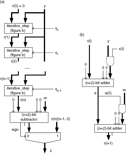
Figure 15.6 Montgomery multiplier.
If ripple adders are used then
![]()
and
Example 15.3 (Complete VHDL source code available.) Generate the VHDL model of a binary (B = 2) Montgomery multiplier:
entity Montgomery_step is
port (
  r: in std_logic_vector(n downto 0);
  y: in std_logic_vector(n-1 downto 0);
  x: in std_logic;
  next_r: out std_logic_vector(n downto 0)
);
end Montgomery_step;

architecture circuit of Montgomery_step is
  signal long_r, y_by_x, a, m_by_a, two_r:
  std_logic_vector(n+1 downto 0);
  signal module: std_logic_vector(n-1 downto 0);
begin
  long_r<=‘0’&r;
  and_gates1: for i in 0 to n-1 generate
    y_by_x(i)<=y(i) and x;
  end generate;
  y_by_x(n)<=‘0’; y_by_x(n+1)<=‘0’;
  a<=long_r+y_by_x;
  module<=conv_std_logic_vector(m, n);
  and_gates2: for i in 0 to n-1 generate
    m_by_a(i)<=module(i) and a(0);
  end generate;
  m_by_a(n)<=‘0’; m_by_a(n+1)<=‘0’;
  two_r<=a+m_by_a;
  next_r<=two_r(n+1 downto 1);
end circuit;

entity Montgomery_multiplier is
port (
  x, y: in std_logic_vector(n-1 downto 0);
  z: out std_logic_vector(n-1 downto 0)
);
end Montgomery_multiplier;

architecture circuit of Montgomery_multiplier is
  component Montgomery_step…end component;
  signal r: r_vector;
  signal module: std_logic_vector(n-1 downto 0);
  signal long_r_n, long_module, dif:
  std_logic_vector(n+1 downto 0);
begin
  module<=conv_std_logic_vector(m, n);
  r(0)<=zero;
  iteration: for i in 0 to n-1 generate
    step: Montgomery_step port map (r(i), y, x(i), r(i+1));
  end generate;
  long_r_n<=‘0’&r(n); long_module<=“00”&module;
  dif<=long_r_n - long_module;
  with dif(n+1) select z<=dif(n-1 downto 0) when ‘0’,
  r(n)(n-1 downto 0) when others;
end circuit;
15.1.2.4 Modulo (Bk-c) Reduction
In the case where m = Bk − c for some small c the modulo m reduction can be performed with Algorithm 8.13. The corresponding cell is shown in Figure 15.7a: z is assumed to be a q-digit number and c a t-digit one. The value of new_z is smaller than the initial value z. After several steps, a number last_z is obtained with the following properties: last_z mod m = x mod m, and last_z < Bn. If m ≥ Bn−1, then x mod m = last_z − q.m for some q < B. The total cost and computation time depend on the number of steps, that is, on the particular values of x and m. An additional one-step divider is necessary in order to generate the final result (Figure 15.7b).
Example 15.4 (Complete VHDL source code available.) Generate the VHDL model of a circuit that computes x modulo 2n − c, x being a 2.n-bit number (e.g., the result of multiplying two n-bit numbers). The structure of the data path is shown in Figure 15.8.
entity data_path is
port (
  x: in std_logic_vector(2*n-1 downto 0);
  clk, sel, enable: in std_logic;
  z: out std_logic_vector(n-1 downto 0);
  equal_zero: out std_logic
);
end data_path;

architecture circuit of data_path is
  signal next_x1, next_x0, x1, x0, y1, y0:
  std_logic_vector(n-1 downto 0);
  signal x1_by_c, long_x0, y: std_logic_vector(2*n-1 downto 0);
  signal long_y0, minus_m, y0_minus_m:
  std_logic_vector(n downto 0);
begin
  with sel select next_x1<=y1 when ‘0’, x(2*n-1 downto n)
  when others;
  with sel select next_x0<=y0 when ‘0’, x(n-1 downto 0)
  when others;
  process(clk)
  begin
    if clk'event and clk=‘1’ then
      if enable=‘1’ then x1<=next_x1; x0<=next_x0; end if;
    end if;
  end process;
  x1_by_c<=x1*conv_std_logic_vector(c, n);
  long_x0<=zero&x0;
  y<=x1_by_c+long_x0;
  y1<=y(2*n-1 downto n); y0<=y(n-1 downto 0);
  equal_zero<=‘1’ when y1=zero else ‘0’;
  long_y0<=‘0’& y0;
  minus_m<=conv_std_logic_vector(2**n - m, n+1);
  y0_minus_m<=long_y0+minus_m;
  with y0_minus_m(n) select z<=y0_minus_m(n-1 downto 0)
  when ‘1’, y0 when others;
end circuit;

entity control_unit is
port (
  clk, reset, start, equal_zero: in std_logic;
  done, sel, enable: out std_logic
);
end control_unit;

architecture rtl of control_unit is
  subtype internal_state is natural range 0 to 3;
  signal state: internal_state;
begin
  process(clk, reset)
  begin
    case state is
      when 0=>sel<=‘1’; enable<=‘0’; done<=‘1’;
      when 1=>sel<=‘1’; enable<=‘0’; done<=‘1’;
      when 2=>sel<=‘1’; enable<=‘1’; done<=‘0’;
      when 3=>sel<=‘0’; enable<=‘1’; done<=‘0’;
  end case;
    if reset=‘1’ then state<=0;
    elsif clk'event and clk=‘1’ then
    case state is
      when 0=>if start=‘0’ then state<=state+1; end if;
      when 1=>if start=‘1’ then state<=state+1; end if;
      when 2=>state<=state+1;
      when 3=>if equal_zero=‘1’ then state<=0;end if;
    end case;
    end if;
  end process;
end rtl;

entity mod_reduction is
port (
  x: in std_logic_vector(2*n-1 downto 0);
  clk, reset, start: in std_logic;
  z: out std_logic_vector(n-1 downto 0);
  done: out std_logic
);
end mod_reduction;

architecture circuit of mod_reduction is
  component data_path…end component;
  component control_unit…end component;
  signal sel, enable, equal_zero: std_logic;
begin
  component1: data_path port map(x, clk, sel, enable, z,
  equal_zero);
  component2: control_unit port map(clk, reset, start,
  equal_zero, done, sel, enable);
end circuit;

Figure 15.7 (a) Mod m reduction cell. (b) Divider.

Figure 15.8 Data path of the modulo (2n − c) reduction circuit.
As was mentioned in Chapter 8, for some particular values of m (still) more specific algorithms can be used.
Example 15.5 (Complete VHDL source code available.) The circuit of Figure 15.9 implements a mod 239 reduction circuit based on the algorithm of Example 8.5.

Figure 15.9 Mod 239 reduction circuit.
Observe that if x = x(15) x(14) … x(0) and x′ = x′(9) x′(8) … x′(0), then

If x can be any 16-bit number, then

15.1.2.5 Exponentiation
The data path of Figure 15.10 allows us to execute Algorithm 8.15. Its cost and computation time are equal to
If ripple-carry adders are used within the Montgomery multiplier, then (15.5):
For large values of n:
Example 15.6 (Complete VHDL source code available.) Generate the VHDL model of a circuit that computes yx modulo m, where x and y are two n-bit numbers. The structure of the data path is shown in Figure 15.10.
entity exp_data_path is
port (
  y: in std_logic_vector(n-1 downto 0);
  sel: in std_logic_vector(1 downto 0);
  clk, enable_e, enable_y: in std_logic;
  z: out std_logic_vector(n-1 downto 0)
);
end exp_data_path;

architecture circuit of exp_data_path is
  signal mult_in1, mult_in2, mult_out, reg_e_in, e_t, y_t,
  exp_n, exp_2n: std_logic_vector(n-1 downto 0);
  component Montgomery_multiplier…end component;
begin
  exp_2n<=conv_std_logic_vector(int_exp_2n, n);
  with sel select mult_in1<=y when “00”, e_t when others;
  with sel select mult_in2<=exp_2n when “00”, e_t when “01”,
  y_t when “10”, one when others;
  multiplier: Montgomery_multiplier
  port map (mult_in1, mult_in2, mult_out);
  exp_n<=conv_std_logic_vector(int_exp_n, n);
  with sel select reg_e_in<=exp_n when “00”, mult_out when
  others;
  process(clk)
  begin
    if clk'event and clk=‘1’ then
    if enable_e=‘1’ then e_t<=reg_e_in; end if;
    end if;
  end process;
  process(clk)
  begin
    if clk'event and clk=‘1’ then
    if enable_y=‘1’ then y_t<=mult_out; end if;
    end if;
  end process;
  z<=e_t;
end circuit;

entity exp_control_unit is
port (
  clk, reset, start: in std_logic;
  x: in std_logic_vector(n-1 downto 0);
  done, enable_e, enable_y: out std_logic;
  sel: out std_logic_vector(1 downto 0)
);
end exp_control_unit;

architecture rtl of exp_control_unit is
  subtype internal_state is natural range 0 to 7;
  signal state: internal_state;
  subtype count is integer range 0 to n-1;
  signal counter: count;
begin
  process(clk, reset)
  begin
    case state is
    when 0=>sel<=“00”; enable_e<=‘0’; enable_y<=‘1’;
    done<=‘1’;
    when 1=>sel<=“00”; enable_e<=‘0’; enable_y<=‘1’;
    done<=‘1’;
    when 2=>sel<=“00”; enable_e<=‘1’; enable_y<=‘0’;
    done<=‘0’;
    when 3=>sel<=“00”; enable_e<=‘0’; enable_y<=‘1’;
    done<=‘0’;
    when 4=>sel<=“01”; enable_e<=‘1’; enable_y<=‘0’;
    done<=‘0’;
    when 5=>sel<=“10”; enable_e<=‘1’; enable_y<=‘0’;
    done<=‘0’;
    when 6=>sel<=“10”; enable_e<=‘0’; enable_y<=‘0’;
    done<=‘0’;
    when 7=>sel<=“11”; enable_e<=‘1’; enable_y<=‘0’;
    done<=‘0’;
  end case;
  if reset=‘1’ then state<=0; counter<=n-1;
  elsif clk'event and clk=‘1’ then
    case state is
      when 0=>if start=‘0’ then state<=state+1; end if;
      when 1=>if start=“1” then state<=state+1; end if;
      when 2=>state<=state+1;
      when 3=>state<=state+1; counter<=n-1;
      when 4=>if x(counter)=‘1’ then state<=state+1;
      else state<=6; end if; counter<=counter - 1;
      when 5=>state<=state+1;
      when 6=>if counter<0 then state<=state+1;
      else state<=4; end if;
      when 7=>state<=0;
    end case;
    end if;
  end process;
end rtl;

entity exponentiate is
port (
  x, y: in std_logic_vector(n-1 downto 0);
  clk, reset, start: in std_logic;
  z: out std_logic_vector(n-1 downto 0);
  done: out std_logic
);
end exponentiate;

architecture circuit of exponentiate is
  component exp_data_path…end component;
  component exp_control_unit…end component;
  signal sel: std_logic_vector(1 downto 0);
  signal enable_e, enable_y: std_logic;
begin
  first_component: exp_data_path port map (y, sel, clk,
  enable_e, enable_y, z);
  second_component: exp_control_unit port map (clk, reset,
  start, x, done, enable_e, enable_y, sel);
end circuit;
