14.1 BASE CONVERSION
14.1.1 General Base Conversion
The general conversion algorithm described in Algorithm 7.1 for natural numbers has a mainly theoretical interest. In the context of general-purpose binary computers, a general circuit to convert n-digit base-B1 numbers into m-digit base-B2 ones doesn't seem to warrant practical interest. A block diagram is nevertheless presented in Figure 14.1 to illustrate a possible implementation of such a circuit, assuming a binary coding for the digits in both bases.
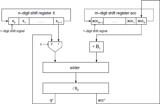
Figure 14.1 Block diagram of a general base converter.
The multiplier by B1, the adder stage, and the divider by B2 are binary operators defined as follows:
- The multiplier-by-B1 has a (1 +
 log2 (B2 − 1)
 )-bit input and a (2 + log2(B2 − 1)+ log2 B1)-bit output.
 - The adder stage inputs are the output of the multiplier, and a (1 + log2 (B1 − 1))-bit digit; the output is a (1 + log2 (B2.B1 − 1))-bit digit.
- The divider-by-B2 input is the output of the adder while the outputs, namely, the quotient q+ and the remainder acc+, are, respectively, (1+ log2 (B1 − 1))-bit and (1 + log2 (B2 − 1))-bit digits.
At the start, the shift register X of Figure 14.1 is loaded with the n-digit base-B1 number to be converted, while the result will be stored in the m-digit shift register acc initially set to zero. Control signals are then generated as follows, according to Algorithm 7.1:
- at the first step (i = 0; j = 0) the multiplexer control signal c is set to 1, then (j ≥ 1) c is reset to 0 until i is incremented (j back to zero);
- each time j is incremented, a shift signal generates a circular 1-digit right-shift of register acc;
- each time j is reset to zero (from m − 1), i is incremented and shift signals generate circular 1-digit right-shifts of both registers X and acc; the multiplexer control signal c is set to 1, then reset to zero as soon as j = 1.
The cost C(n, m) and computation time T(n, m) of the implementation suggested by Figure 14.1 are
where m is such that
m is thus computed as
14.1.2 BCD to Binary Converter
14.1.2.1 Nonrestoring 2p Subtracting Implementation
To make sense, this implementation assumes that the successive powers of 2 are expressed in BCD and that a BCD subtractor is available. Figure 14.2 presents a block diagram of a possible implementation. The BCD-coded 2p (p = 0, 1, … , n − 1) may be read from a look-up table. The allowed range for a given BCD number X is
that is,
![]()
Figure 14.2 presents a combinational (part (a)) and a sequential (part (b)) implementation circuit. In both instances, the successive BCD powers of 2 have to be generated. The sequential circuit requires a multiplexer to initialize the process by loading the data XBCD. The complemented successive sign-bits are the desired binary components of X.
The cost C(n) and computation time T(n) of the combinational implementation suggested by Figure 14.2a are (excluding registers)

Figure 14.2 Nonrestoring BCD to binary converter.
For the sequential implementation, the computation time behavior is roughly the same while the cost C(n) is reduced to
14.1.2.2 Shift-and-Add BCD to Binary Converter
According to the first step of Algorithm 7.2, the leftmost BCD digit is multiplied by ten and added to the next right neighbor digit. The next iteration steps then consist of multiplying the successive results by ten and adding the next right neighbor digit. Multiplication by ten (binary coded 1010) is handled by a double shift as illustrated in the following.
where X(i) is a 4-bit binary number (BCD code). The current step i is then completed by adding X(i − 1) to the result.
A customized multiplier by ten can be designed or, alternatively, operation (14.7) can be handled by a 2-bit shift, a sum, and a 1-bit shift. Figure 14.3 depicts a 2-adder circuit to carry out the elementary step:
Figure 14.3 Shift-and-add BCD to binary converter: elementary step.
Figure 14.4 presents a combinational (part (a)) and a sequential (part (b)) implementation circuit. The sequential circuit requires a multiplexer to initialize the process by loading the data XBCD(m − 1). The cost C(m) and computation time T(m) of the combinational implementation of Figure 14.4a are
For the sequential implementation the computation time behavior is roughly the same while the cost C(n) is reduced to
Formula (14.3) for B2 = 10 and B1 = 2 gives
Thus, comparing formulas (14.9) to (14.5), we find better cost and computation time behaviors for the shift-and-add implementation. Moreover, the binary adder is simpler than the BCD adder-subtractor needed in the nonrestoring implementation of Section 14.1.2.1.

Figure 14.4 Shift-and-add BCD to binary converter.
14.1.3 Binary to BCD Converter
The binary-to-BCD conversion procedure described by Algorithm 7.3 basically consists in doubling the BCD partial result bcd(i) and adding the next bit from the binary expression to be converted. Two basic procedures have to be defined:
- Add a 1-bit number to a BCD number.
- Multiplication by two of a BCD number.
Since the binary digit x also stands for the BCD number 000x, the first procedure is just a straight BCD sum. The multiplication by two is less straightforward for BCD numbers than for binary numbers (shift). The procedure BCDx2_step, described in Chapter 7, may be carried out in parallel on each BCD digit. Assuming that each digit is 1-bit left shifted, a carry is computed and set to 0 whenever the shifted digit is not greater than 9; otherwise the carry is set to 1 and a correction of (0110)2 is added modulo 16 to the shifted BCD digit. The computed carry can be used to feed the correction input of the mod 16 adder. Since the next left neighbor digit has also been 1-bit shifted, the carry will stand at the rightmost position of the next digit without generating carry propagation. The Boolean expression (Chapter 7)
generates a carry y(i + 1)0 = 0 whenever the BCD digit X(i) is not greater than 4, that is,
![]()
y(i + 1)0 = 1 otherwise. Figure 14.5a shows the carry circuit. Figure 14.5b displays the BCDx2_step circuit.
The circuits of Figure 14.6 implement the full conversion process described in Algorithm 7.3. Observe that the first three steps are trivial, so one can initialize the computation scheme with the partial result bcd(n − 3) = (0 xn−1 xn−2 xn−3); the next partial results bcd(n − j) are then iteratively multiplied by two and added to (0 0 0 xn−j−1). The cost C(n) and computation time T(n) of the combinational implementation of Figure 14.6a are
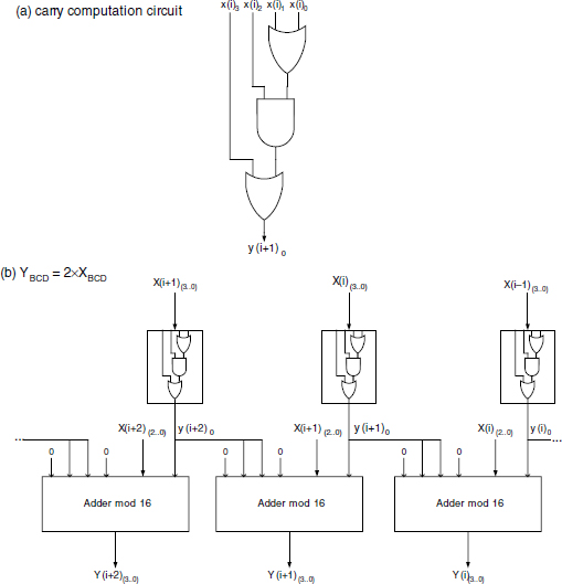
Figure 14.5 BCDx2_step implementation circuit.

Figure 14.6 BCD to binary converter.
For the sequential implementation (Figure 14.6b) the computation time behavior is roughly the same while the cost C(n) is reduced to
The relation (14.11) between m and n still holds.
14.1.4 Base-B to RNS Converter
be an n-digit B-ary number to be converted in a RNS system defined by the non redundant set of moduli {mj}, j = 1,2, …, s. One assumes that
otherwise the conversion would be modulo M.
The most straightforward circuit to convert base-B to RNS consists of a set of dividers by the respective moduli mj (Figure 14.7). The remainders Rj are the desired RNS components: results of the successive reductions modulo mj. The design problem is thus that of the synthesis of integer dividers by mj. Optimization techniques generally start from the selection of the set of moduli. As quoted in Chapters 8 and 15, specific moduli can lead to better algorithms and higher performance implementations.
The converter circuit presented in Figure 14.8 implements Algorithm 7.4. It is assumed that the xi and mj are binary coded, as well as the outputs: RNS components rj, and Rj. The circuit first computes the RNS expressions of xi.Bi (i = 0, 1, … , n − 1) then adds them. This operation corresponds to s multioperand additions mod mj (j = 0, 1, … , s).
The n.s values rj(i) of (xi.Bi) mod mj are read from n look-up tables LUTi such as those displayed in Figure 7.1 to illustrate Example 7.5. Since the factor Bi is implicit, only ![]() log2(B)
log2(B)![]() ) binary inputs are needed to address any LUTi and Σj(
) binary inputs are needed to address any LUTi and Σj(![]() log2 (mj)
log2 (mj)![]() ) binary outputs are required to code the RNS expression of (xi.Bi). The size CLUT of LUTi, expressed as a number of binary entries, is given by
) binary outputs are required to code the RNS expression of (xi.Bi). The size CLUT of LUTi, expressed as a number of binary entries, is given by

Figure 14.7 Base-B to RNS converter.
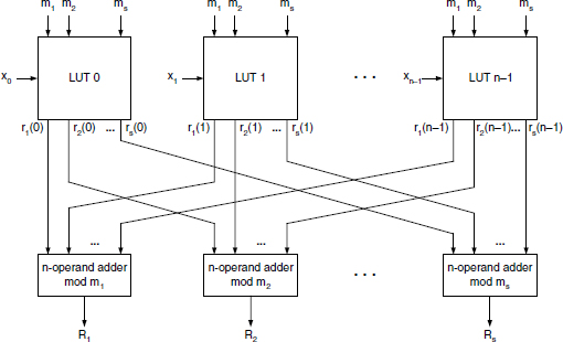
Figure 14.8 Base-B to RNS converter using LUTs.
The n-operand adder mod mj can be designed as a tree of 2-operand adders. From the cost and computation time point of view, the choice of the modulus set is critical. The cost C(n, s) and computation time T(n, s) of the circuit presented in Figure 14.8 are
14.1.5 CRT RNS to Base-B Converter
The implementation proposed in this section is based on the Chinese remainder theorem (Algorithm 7.6); it is assumed that {![]() } and {(1/
} and {(1/![]() ) mod mi} are available from look-up tables. The circuit presented in Figure 14.9 is made up of s multipliers mod M, s multipliers mod mj (j = 1, 2, … , s), and 1 multioperand adder mod M.
) mod mi} are available from look-up tables. The circuit presented in Figure 14.9 is made up of s multipliers mod M, s multipliers mod mj (j = 1, 2, … , s), and 1 multioperand adder mod M.
If binary coding is assumed, log2 mi bits will be required for the inputs and outputs of the respective multipliers mod mj, and log2 M bits for the multipliers mod M and the multioperand adder mod M. The cost C(M, s) and computation time T(M, s) of the circuit presented in Figure 14.9 are

Figure 14.9 CRT RNS to base-B converter.
The size of the look-up tables is bounded by s.log2 m bits (m is the greatest modulus).
Given the range M, a set of pairwise prime moduli {mi} may be selected as minimal according to some particular criterion ([GAR1959], [SZA1967]). So if a strategy is defined to select the set of moduli from a given range M, the cost and time complexity can actually be computed as a function of M only.
If a parameterized circuit can be synthesized to achieve mod mi multiplication, a low-cost iterative sequential circuit can be designed (Figure 14.10).
The cost C(M, s) and computation time T(M, s) of the circuit presented in Figure 14.10 are roughly
where m stands for the greatest modulus of the set {mj}. It is assumed that

Figure 14.10 CRT RNS to base-B sequential converter.
The preceding examples emphasize the fact that RNS converter design mainly consists of finite field operator design (Chapters 8 and 15). Nevertheless, this result may be seen as a part of the more general problem coming out of the complete design of a RNS system; this involves the modulus set selection, the RNS arithmetic unit design, and the coding–decoding process implementation. Typically, modulus selection plays a prominent role in the complexity of RNS arithmetic operators, including coding–decoding units. Special moduli such as Mersenne numbers, 2n − 1 or more generally Bn − c, with c ![]() Bn (Chapter 8), are often considered; as quoted before carefully selected moduli can lead to specific algorithms for which implementations can be derived with better time/cost characteristics.
Bn (Chapter 8), are often considered; as quoted before carefully selected moduli can lead to specific algorithms for which implementations can be derived with better time/cost characteristics.
14.1.6 RNS to Mixed-Radix System Converter
Since the conversion from mixed-radix system to base-B is straightforward, the following implementation can be set to achieve the RNS to base-B conversion.
According to Chapters 3 and 7, let
be a mixed-radix expression in a system defined by the set of radices {b0, b1, …, bn−1} setting down the set of weights {B0, B1, …, Bn−1} such that B0 = 1 and
The mixed-radix digit_extraction algorithm 7.7 achieves the conversion from a source RNS system with a set of moduli {mi} to a target mixed-radix system with the same set {mi} as radix set. The mi do not need to be ordered by size or whatever; that same order must be respected for both source and target systems. Nevertheless, ordering the residues ri from left to right, by decreasing the size of the mi, makes trivial the iterative RNS coding of the successive residues with respect to the left side moduli, as required by substep 2 of each iteration step. In the iterative circuit, presented in Figure 14.11, the initial RNS expression is denoted R1(s..1), assuming ![]() such that i > j. The first mixed-radix digit x0 (substep 1) is readily extracted as R1(1). The next stage (substep 2) achieves the RNS subtraction R1(s..1) − R1(1); as the mi are ordered by increasing size from right to left,
such that i > j. The first mixed-radix digit x0 (substep 1) is readily extracted as R1(1). The next stage (substep 2) achieves the RNS subtraction R1(s..1) − R1(1); as the mi are ordered by increasing size from right to left, ![]() the RNS components of R1(1) are repeatedly R1(1). The third stage (substep 3) divides its RNS input R2(s..2) by m1: this operation is achieved through componentwise multiplication mod mi>1 of R2(i) by (1/m1) mod mi. From the result
the RNS components of R1(1) are repeatedly R1(1). The third stage (substep 3) divides its RNS input R2(s..2) by m1: this operation is achieved through componentwise multiplication mod mi>1 of R2(i) by (1/m1) mod mi. From the result ![]() (s..2), the next mixed-radix digit x1 is extracted as
(s..2), the next mixed-radix digit x1 is extracted as ![]() (2). Step k starts with input
(2). Step k starts with input ![]() (s..k); xk−1 is first extracted as
(s..k); xk−1 is first extracted as ![]() (k) then (substep 2) the subtracter computes
(k) then (substep 2) the subtracter computes ![]() the third substep finally multiplies Rk+1(s..k + 1) by 1/mk through componentwise multiplication mod mi>k of Rk+1(i) by (1/mk) mod mi.
the third substep finally multiplies Rk+1(s..k + 1) by 1/mk through componentwise multiplication mod mi>k of Rk+1(i) by (1/mk) mod mi.
Example 14.1 This example illustrates a converter for a RNS source system with the following set of 6 (s) moduli (ordered by size) defining a range of 23881935:
The LUT design is first tackled by computing the inverses of mi modulo mj>i. Table 14.1 displays the contents of the LUTs related to the respective (1/mi).
According to Figure 14.11, the specific circuit can be built with 5 (s − 1) sets (LUT + subtractor + multiplier) as shown in Figure 14.12, where a numeric example is worked out. The source RNS expression is given as R1 = (11, 10, 9, 8, 7, 6) for which the target mixed-radix expression is computed as X = (12, 22, 3, 3, 8, 6).

Figure 14.11 RNS to mixed-radix system converter.
TABLE 14.1 Inverse (1/mi) mod mj>i

The mixed-radix system weights, computed from (14.24), are
![]()
from which the decimal value of X can be computed as 9832808.
If standard LUT and RNS operators are used, the cost C(s) and computation time T(s) of the circuit presented in Figure 14.11 are
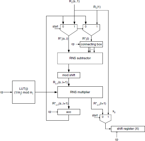
otherwise, the sizes of the operators may decrease step by step as appears in figures 14.11 and 14.12. Observe that the sizes of the moduli are also involved in the overall complexity. The sequential implementation of the circuit depicted in Figure 14.11 is given in figure 14.13. In that case, the maximum size is required for the subtractor and multiplier units. Three multiplexers are used to initialize the process with the source RNS expression R1(s..1), and to extract the first mixed-radix digit x0. As the size (number of residues) of ![]() (s..i) decreases step by step after each subtraction, a special mod shift operator is needed to adjust the result Ri+1(s..i + 1) before the multiplier stage. In the same way, a connecting box sets the connections
(s..i) decreases step by step after each subtraction, a special mod shift operator is needed to adjust the result Ri+1(s..i + 1) before the multiplier stage. In the same way, a connecting box sets the connections ![]() (i) to the subtractor. The cost C(s, m) and computation time T(s, m) of the circuit presented in Figure 14.13 are
(i) to the subtractor. The cost C(s, m) and computation time T(s, m) of the circuit presented in Figure 14.13 are
where m stands for the greatest modulus ms.
For practical implementations, binary coding is used for residues and moduli; so standard digital cells may be used to synthesize all the elements of Figures 14.11 to 14.13. Observe that the circuits presented are conceptually independent of the coding selected; the available technology will lead the choice.