12.1 NATURAL NUMBERS
12.1.1 Basic Multiplier
According to the Hörner expansion presented in Chapter 5, formula (5.6),
![]()
is easily mapped into a combinational circuit to materialize Algorithm 5.2 (shift and add 2). A basic space iteration of the shift and add multiplier in base B is shown in Figure 12.1. The function Z implemented by this n-digit × m-digit multiplier is
![]()
where D = P(0) is an m-digit number.
Whenever B > 2, the size of the result Z is m + n; moreover, (m + 1)-digit adders are needed, because xi.Y may exceed Bm − 1. Otherwise, in the binary case, the size of the result is limited to m + n − 1, and m-digit adders meet the requirement. After each addition step, a digit result appears as the rightmost digit of the shifted sum. According to the case at hand, inverting the role of multiplicand and multiplicator may appear useful. The effects of this permutation are that the products yi.X are n-digit products (instead of m for xi.Y), while the n (m + 1)-digit adders are switched for m (n + 1)-digit ones. Obviously the size of the result doesn't change.
The hardware cost of this circuit is high because of the n (resp. m) adders involved. The time is roughly equal to n (m + 1)-digit (resp. m (n + 1)-digit) adders. As will be observed later, if ripple-carry adders are used, this implementation reduces to the ripple-carry multiplier (Section 12.1.3.1).
Example 12.1 (Complete VHDL source code available.) Generate a generic n-digit by m-digit base-B basic multiplier. The first multiplier step called is mult_by_1_digit:
 entity mult_by_1_digit is
 Port (
   A: in digit_vector(M-1 downto 0);
   B: in digit_vector(M-1 downto 0);
   x_i: in digit;
   P: out digit_vector(M downto 0)
   );
 end mult_by_1_digit;

 architecture Behavioral of mult_by_1_digit is
 begin
   process(B, A, x_i)
   variable carry: digit_vector(M downto 0);
   begin
 carry(0):=0;
 for i in 0 to M-1 loop
   P(i)<=(B(i)*X_i+A(i)+carry(i)) mod BASE;
   carry(i+1):=(B(i)*X_i+A(i)+carry(i))/BASE;
 end loop;
 P(M)<=carry(M);
  end process;
end Behavioral;

Figure 12.1 Basic base-B multiplier.
The multiplier structure of Figure 12.1 is:
 entity basic_base_B_mult is
 port (
   X: in digit_vector(N-1 downto 0);
   Y: in digit_vector(M-1 downto 0);
   P: out digit_vector(N+M-1 downto 0)
   );
 end basic_base_B_mult;

 architecture simple_arch of basic_base_B_mult is
   type connections is array (0 to N) of digit_vector(M downto 0);
  signal wires: connections;
 begin
  wires(0)<=(others=>0);
  iterac: for i in 0 to N-1 generate
    mult: mult_by_1_digit port map (wires(i)(M downto 1),
       Y, X(i), wires(i+1));
    p(i)<=wires(i+1)(0);
  end generate;
  p(M+N-1 downto N)<=wires(N)(M downto 1);
end simple_arch;
Example 12.2 (Complete VHDL source code available.) Generate a generic n-bit by m-bit base-2 basic multiplier. The first multiplier step called is mult_by_1_bit:
 entity mult_by_1_bit is

 Port (
   A: in std_logic_vector (M-1 downto 0);
   B: in std_logic_vector (M-1 downto 0);
   X_i: in std_logic;
   S: out std_logic_vector (M downto 0)
   );
end mult_by_1_bit;

architecture Behavioral of mult_by_1_bit is
begin
  add_mux: process(x_i,A,B)
  begin
    if x_i=‘1’ then
      S<=(‘0’ & A)+B;
    else
       S<=(‘0’ & A);
     end if;
   end process;
end Behavioral;
The multiplier structure is:
 entity basic_base2_mult is
 port (
   X: in std_logic_vector (N-1 downto 0);
   Y: in std_logic_vector (M-1 downto 0);
   P: out std_logic_vector (N+M-1 downto 0)
   );
end basic_base2_mult;

architecture simple_arch of basic_base2_mult is
type connect is array (0 to N) of std_logic_vector (M downto 0);
signal wires: connect;
begin
  wires(0)<=(others=>‘0’);
  iterac: for i in 0 to N-1 generate
    mult: mult_by_1_bit port map (wires(i)(M downto 1), Y, X(i),
    wires(i+1));
    p(i)<=wires(i+1)(0);
  end generate;
  p(M+N-1 downto N)<=wires(N)(M downto 1);
end simple_arch;
12.1.2 Sequential Multipliers
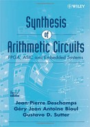
Shift and add Algorithms 5.1 and 5.2 are actually more suited for time iteration, that is, using the same adder recursively. As an example, a sequential multiplier derived from Algorithm 5.2 is shown in Figure 12.2. Initially, the n-digit shift register contains X. If the m-digit register is preset to P(0) = D then Z = X.Y + D after n clock cycles.
12.1.3 Cellular Multiplier Arrays
Most combinational multipliers belong to the class of multiplication arrays. An essential characteristic of multiplication arrays is that they rest on computation primitives that are independent of the data size. The multiplication process consists of two main phases: in the first phase, the digit-by-digit products xiyj are computed; in the second phase, the addition phase, those products are added. These phases are not necessarily successive. According to the type of implementation some mix can happen between making products and adding them. This occurs typically when a reduced set of cells is used sequentially. Most multiplication arrays start from the basic pencil and paper scheme described in Chapter 5, Figure 5.1. Actually, in the literature, the cell arrays are generally presented according to this scheme, obviously not related to the place and route process result in the physical circuits. Most often, partial products are represented by simple dots, whose coordinates (i, j) in the scheme stand for the actual indices of the digit product being represented.
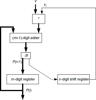
Figure 12.2 Sequential base-B shift and add multiplier.
Example 12.3 (Complete VHDL source code available.) Generate a generic n-digit by m-digit base-B basic sequential multiplier. The basic cell mult_by_1_digit is similar as in Example 12.1. The circuit of Figure 12.2 including the state machine is:
 entity basic_base_B_mult_seq is
 port (
   clk: in std_logic;
   ini: in std_logic;
   X: in digit_vector(N-1 downto 0);
   Y: in digit_vector(M-1 downto 0);
   done: out std_logic;
   P: out digit_vector(N+M-1 downto 0)
   );
 end basic_base_B_mult_seq;

 architecture simple_seq_arch of basic_base_B_mult_seq is
   signal reg_X: digit_vector(N-1 downto 0);
   signal reg_Y, reg_P: digit_vector(M-1 downto 0);
   signal n_reg_P: digit_vector(M downto 0);
   signal counter: integer range 0 to N+1;
   signal work: std_logic;
 begin
   state_mach: process (clk, work, ini)
   begin
     if clk’event and clk=‘0’ then
       if ini=‘1’ then
         work<=‘1’; counter<=0;
         reg_P<=(others=>0);
         reg_X<=X; reg_Y<=Y;
       elsif work=‘1’ then
         counter<=counter+1;
         reg_P<=n_reg_P(M downto 1);
         reg_X<=n_reg_P(0) & reg_X(N-1 downto 1);
         if (counter=N) then
           P<=reg_P & reg_X;
           work<=‘0’;
         end if;
       end if;
     end if;
   end process;
   mult: mult_by_1_digit port map (reg_P,reg_Y,reg_X(0),n_
   reg_P);
   done<=not work;
 end simple_seq_arch;
12.1.3.1 Ripple-Carry Multiplier
The space iteration of Algorithm 5.4 (cellular ripple-carry algorithm) is materialized by the combinational circuit displayed in Figure 12.4. The basic cell (Figure 12.3) computes
![]()
and
![]()
The implementation of the basic cell depends on the cost/speed trade-off to be considered by the designer. A full-custom high-speed circuit option would suggest, for binary-coded digits (e.g., high-radix or binary-coded decimal—BCD), a look-up table procedure or a 3-level combinational implementation. In the case of BCD digits, the problem at hand is that of a simultaneous synthesis of eight 16-variable functions. Thanks to the symmetry, this problem is affordable but the hardware cost could be prohibitive compared to the one suggested by Figure 12.3b with standard adders and multipliers or using FPGA. The circuit of Figure 12.4 displays the ripple-carry array for an n-digit × m-digit multiplier. It is the direct mapping of the precedence graph presented in Chapter 5, Figure 5.2.

Figure 12.3 Basic cell: (a) symbol and (b) details.

Figure 12.4 Ripple-carry multiplier.
Comment 12.1 In base 2, the circuit of Figure 12.3b is reduced to an AND (carry-free) gate for the binary product and a base-2 full adder. Although this could suggest a cell implementation with one additional gate delay, classic synthesis techniques readily provide 3-level implementations at a reasonable cost.
Example 12.4 (Complete VHDL source code available.) Generate a generic n-bit by m-bit base-2 ripple-carry multiplier. The first multiplier cell (Figure 12.3b) is:
 entity basic_mul_cell is
 Port (
   x_i, y_j: in std_logic;
   cin, pin: in std_logic;
   cout, pout: out std_logic;
   );
 end basic_mul_cell;

 architecture behavioral of basic_mul_cell is
   signal int_p: std_logic;
 begin
   int_and<=x_i and y_j;
   cout<=(cin and pin) or (cin and int_p) or (pin and int_p);
   pout<=cin xor int_p xor pin;
 end behavioral;
The multiplier structure (Figure 12.4) is:
 entity ripple_carry_mult is
 Port (
   X: in std_logic_vector(N-1 downto 0);
   Y: in std_logic_vector(M-1 downto 0);
   P: out std_logic_vector(M+N-1 downto 0));
 end ripple_carry_mult;

 architecture behavioral of ripple_carry_mult is

 component basic_mul_cell

 type connect is array (0 to N) of std_logic_vector
 (M downto 0);
 signal cin, pin, cout, pout: connect;
 begin
  init: for i in 0 to N-1 generate cin(i)(0)<=‘0’; end generate;
  pin(0)<=(others=>‘0’);
  ext_loop: for i in 0 to N-1 generate
   int_loop: for j in 0 to M-1 generate
    cell: basic_mul_cell port map(X(i), Y(j),
       cin(i)(j), pin(i)(j), cout(i)(j), pout(i)(j));
    cin(i)(j+1)<=cout(i)(j);
    j0: if j=0 generate p(i)<=pout(i)(j); end generate;
    jn: if j>0 generate pin(i+1)(j-1)<=pout(i)(j); end generate;
   end generate;
   pin(i+1)(M-1)<=cin(i)(M);
   end generate;
   P(M+N21 downto N)<=pin(N)(M-1 downto 0);
 end behavioral;
12.1.3.2 Carry-Save Multiplier
The space iteration of Algorithm 5.5 is materialized by the combinational circuit displayed in Figure 12.5. The basic cell now computes
![]()
and
![]()
This is a straightforward application of the carry-save technique of Chapter 11 (Figure 11.40). A carry-save multiplier, with m = n, is shown in Figure 12.5.
The basic cell is the same as that of Figure 12.3a, with a single difference: the carry output (ci(j+1) in the ripple-carry array) is now indexed as c(i+1)j. This means that this carry is now connected as input to cell (i + 1, j), instead of cell (i, j + 1) for the ripple-carry. This reindexing technique corresponds to new connection assignments as it appears in Figure 12.5. Basically the array is similar to the ripple-carry one with respect to the number of cells but an additional n-bit adder is necessary at the bottom of the array. Observe that, due to the maximum length of the result, the leftmost half-adder has carry necessarily zeroed; this module may accordingly be reduced to a single XOR gate. As will be shown in the following section, the time saving of the carry-save array with respect to the ripple-carry one is asymptotically 33.3%, while the cost increase remains negligible (n).

Figure 12.5 Carry-save multiplier.
Example 12.5 (Complete VHDL source code available.) Generate a generic n-bit by m-bit base-2 carry-save multiplier. The multiplier cell (Figure 12.3b) is the same as in Example 12.4. The multiplier structure (Figure 12.5) is:
 entity carry_save_mult is
 Port (
   X: in std_logic_vector(N-1 downto 0);
   Y: in std_logic_vector(M-1 downto 0);
   P: out std_logic_vector(M+N-1 downto 0));
 end carry_save_mult;

 architecture behavioral of carry_save_mult is

 type connect is array (0 to N) of std_logic_vector (M downto 0);
 signal cin, pin, cout, pout: connect;
 begin
   pin(0)<=(others=>‘0’); cin(0)<=(others => ‘0’);
   ext_loop: for i in 0 to N-1 generate
    int_loop: for j in 0 to M-1 generate
     cell: basic_mul_cell port map(X(i), Y(j),
        cin(i)(j), pin(i)(j), cout(i)(j), pout(i)(j));
      cin(i+1)(j)<=cout(i)(j);
      j0:if j=0 generate p(i)<= pout(i)(j); end generate;
      jn:if j>0 generate pin(i+1)(j-1)<=pout(i)(j); end generate;
    end generate;
    pin(i+1)(M-1)<=‘0’;
  end generate;
  P(M+N-1 downto N)<= pin(N)(M-1 downto 0)+cin(N)(M-1 downto 0);
end behavioral;
12.1.3.3 Figures of Merit
Assuming that T2 and C2 are the respective time and gate complexity of the standard cells displayed in Figure 12.3, the ripple-carry (n-digit × n-digit) multiplier has overall figures given by:
while the carry-save implementation scheme gives
(the same cost C2 is assumed for the half and full adder cells).
Moreover, if the adding stage is implemented through a fast adding technique, formula (12.3) can be improved.
12.1.4 Multipliers Based on Dissymmetric Br × Bs Cells
This section is a generalization of multiplier arrays to dissymmetric multiplication cells. First, a particular case is treated with xi and yj as 2-digit and 4-digit base-B numbers, respectively; in base 2 it corresponds to radix-16 by radix-4 multiplication. The elementary unit computes a 2-digit carry
and a 4-digit sum
A possible implementation is shown in Figure 12.6, where GHA and GFA are generalized half-adder (two 2-digit operands), and full adder (three 2-digit operands) respectively. Figure 12.7 illustrates a typical array for a 12-digit × 6-digit ripple-carry multiplication with additive operands; for clarity, inputs related to xi and yj have been omitted.
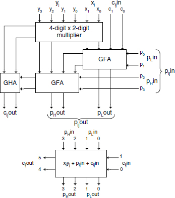
Figure 12.6 A 4-digit × 2-digit multiplication cell.
In Figure 12.7 the digits of the additive operands C and D are displayed at the top and right inputs of the array. The construction is self-explanatory and can readily be expanded to 4m-digit by 2n-digit arrays. Figure 12.7 shows that the concepts of carry and sum, as defined at formulas (12.5) and (12.6), are somewhat artificial; as a matter of fact, one could have defined a 4-bit carry and a 2-bit sum. Each file of cells behaves as a ripple-carry adder producing xi.Y + ci + Pi in, shifted 2 positions to the left with respect to the preceding file.
A carry-save array can be derived but the interconnection structure is somewhat more irregular than that of base-2 multiplications, as it appears in Figure 12.8a. As in the preceding array, inputs corresponding to xi and yj have been omitted; cell inputs and outputs have been labeled according to the exponent of the corresponding power of B weights. The cell inputs and outputs can be, expressed respectively, as
![]()
and
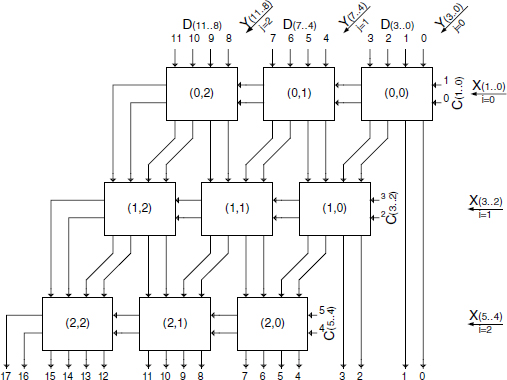
Figure 12.7 Multiplication ripple-carry array using 4-digit by 2-digit cells—X.Y + C + D.
where coefficients of powers of B are 2-digit numbers. So with regard to cell coordinates (i, j), the input and output labels are set, respectively, as
![]()
and
![]()
To make the drawing simpler, inputs and outputs have been reorganized according to the cell presented in Figure 12.8b. The overall circuit is shown in Figure 12.8c; it is strictly equivalent to the one presented in Figure 12.8a.
Observe that a ripple-carry adder has been selected for adding the two numbers provided after the carry-save reduction. This alternative is arbitrary; the choice of the adder type is left to the designer.
Application of carry-save reduction to arbitrary m-digit by n-digit cells is manageable but circuits are less regular.


Figure 12.8 (a) Multiplication carry-save array using 4-digit by 2-digit cells—X.Y + C + D. (b) Carry-save cell, input-output settings, (c) Multiplication carry-save array using 4-digit by 2-digit cells—X.Y + C + D.
Example 12.6 (Complete VHDL source code available.) Generate a generic n-bit by m-bit base-2 ripple-carry multiplier using a 4 by 2 digits multiplier cell. The basic 4 × 2 bits multiplier cell (Figure 12.6) is:
 entity mul_4x2_cell is
 Port (
   x_i: in std_logic_vector(1 downto 0);
   y_j: in std_logic_vector(3 downto 0);
   cin: in std_logic_vector(1 downto 0);
   din: in std_logic_vector(3 downto 0);
   cout: out std_logic_vector(1 downto 0);
   dout: out std_logic_vector(3 downto 0));
 end mul_4x2_cell;

 architecture behavioral of mul_4x2_cell is
 signal int_prod, int_result: std_logic_vector(5 downto 0);
 begin
   int_prod<=x_i*y_j;
   int_result<=int_prod+cin+din;
   dout<=int_result(3 downto 0);
   cout<=int_result(5 downto 4);
 end behavioral;
The multiplier structure (Figure 12.7) is:
package mypackage is
  constant HORZ_CELL: natural:=2;
  constant VERT_CELL: natural:=5;
  constant N: natural:=VERT_CELL*2;
  constant M: natural:=HORZ_CELL*4;
end mypackage;

entity ripple_carry_4x2_mult is
Port (
  X: in std_logic_vector(N-1 downto 0);
  Y: in std_logic_vector(M-1 downto 0);
  P: out std_logic_vector(M+N-1 downto 0));
end ripple_carry_4x2_mult;

architecture behavioral of ripple_carry_4x2_mult is
  type connect_x2 is array (0 to VERT_CELL, 0 to HORZ_CELL) of
  std_logic_vector (1 downto 0); signal cin, cout: connect_x2;
  type connect_x4 is array (0 to VERT_CELL, 0 to HORZ_CELL) of
  std_logic_vector (3 downto 0); signal din, dout: connect_x4;
begin
iniH: for i in 0 to HORZ_CELL-1 generate
  din(0, i)<=“0000”; end generate;
iniV: for i in 0 to VERT_CELL-1 generate
  cin(i, 0)<=“00”; end generate;

ext_loop: for i in 0 to VERT_CELL-1 generate
  int_loop: for j in 0 to HORZ_CELL-1 generate
    cell: mul_4x2_cell port map(
        X((i+1)*2-1 downto i*2),Y((j+1)*4-1 downto j*4),
        cin(i,j), din(i,j), cout(i,j), dout(i,j));
    cin(i,j+1)<=cout(i,j);
    j_0: if j=0 generate
    P((i+1)*2-1 downto i*2)<=dout(i,j)(1 downto 0);
    din(i+1,j)(1 downto 0)<=dout(i,j)(3 downto 2);
  end generate;

  jn0: if j>0 generate
    din(i+1,j-1)(3 downto 2)<=dout(i,j)(1 downto 0);
    din(i+1,j)(1 downto 0)<=dout(i,j)(3 downto 2);
    end generate;
  end generate;
  din(i+1,HORZ_CELL-1)(3 downto 2)<=cin(i,HORZ_CELL);
end generate;

outp_loop: for i in 0 to HORZ_CELL-1 generate
  P((i+1)*4+N-1 downto i*4+N)<=din(VERT_CELL,i);
  end generate;
end behavioral;
Example 12.7 (Complete VHDL source code available.) Generate a generic n-bit by m-bit sequential multiplier for signed operands. The basic multiplier cell is:
entity mult_by_1_bit is
Port (
  A: in std_logic_vector(M-1 downto 0);
  B: in std_logic_vector(M-1 downto 0);
  op: in std_logic; - -(add/sub)=1 or nothing
  a_s: in std_logic; - -add or subtract
  P: out std_logic_vector(M downto 0)
  );
end mult_by_1_bit;

architecture behavioral of mult_by_1_bit is
begin
  process(B, A, op, a_s)
  begin
    if op=‘1’ then
      if a_s=‘0’ then P<=(A(M-1) & A)+(B(M-1) & B);
      else P<=(A(M-1) & A)-(B(M-1) & B);
      end if;
    else P<=(A(M-1) & A);
    end if;
  end process;
end behavioral;
The multiplier including the state machine is:
 entity signed_mult_seq is
 port (
   clk: in std_logic;
   ini: in std_logic;
   X: in std_logic_vector(N-1 downto 0);
   Y: in std_logic_vector(M-1 downto 0);
   done: out std_logic;
   P: out std_logic_vector(N+M-1 downto 0)
   );
 end signed_mult_seq;

 architecture simple_seq_arch of signed_mult_seq is
   signal reg_X: std_logic_vector(N-1 downto 0);
   signal reg_Y, reg_P: std_logic_vector(M-1 downto 0);
   signal n_reg_P: std_logic_vector(M downto 0);
   signal counter: integer range 0 to N;
   signal work, add_sub: std_logic;
 begin
   state_mach: process (clk, work, ini)
   begin
     if clk’event and clk=‘0’ then
       if ini=‘1’ then
         work<=‘1’; add_sub<=‘0’;
         counter<=0;
         reg_X<=X; reg_Y<=Y; reg_P<=(others => ‘0’);
       elsif work=‘1’ then
         counter<=counter+1;
         reg_P<=n_reg_P(M downto 1);
         reg_X<=n_reg_P(0) & reg_X(N-1 downto 1);
         if (counter=N-2) then
           add_sub<=‘1’;
         end if;
         if (counter=N-1) then
            P<=n_reg_P & reg_X(N-1 downto 1);
            work<=‘0’;
         end if;
       end if;
     end if;
  end process;
  done<=not work;
  mult: mult_by_1_bit port map (reg_P, reg_Y,
               reg_X(0), add_sub, n_reg_P);
 end simple_seq_arch;
12.1.5 Multipliers Based on Multioperand Adders
A straightforward way to translate relation (5.4) to a multiplication circuit consists of (i) generating all (shifted) products xn−1.Y.Bn−1, xn−2.Y.Bn−2, …, x2.Y.B2, x1.Y.B, x0.Y and (ii) adding them. The corresponding circuit structure is shown in Figure 12.9.
The multioperand adder can be synthesized according to any one of the methods proposed in Section 11.1.12: carry-save array, carry-save tree (Wallace/Dadda tree) ([WAL1964], [DAD1965]), (p, k)-counter-based adders, and ripple-carry multioperand adders.
Examples 12.8
- An 8-bit × 7-bit multiplier using carry-save tree.
Multioperand adding techniques, as described in Chapter 11, are used to perform a 2-stage reduction tree followed by a 2-operand sum. Parallel counters up to (7,3) are used at the first stage, in such a way that the second stage provides two operands using full adders and half-adders only. Figure 12.10 shows the dot diagram while Figure 12.11 displays the carry-save tree according to Section 11.1.12.4. The detailed circuit is shown in Figure 12.12.
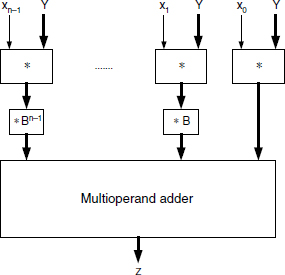
Figure 12.9 Multiplier structure.

Figure 12.10 An 8-bit × 7-bit multiplier: dot diagram.
2. 8-bit × 7-bit multiplier using one-stage carry-save tree with (2, 3; 3), (1, 5; 3), (6, 3), (7, 3) counters and a 3-operand ripple-carry adder made up of parallel counters.

Figure 12.11 An 8-bit × 7-bit multiplier: 7-operand carry-save tree.

Figure 12.12 An 8-bit × 7-bit multiplier circuit.

Figure 12.13 An 8-bit × 7-bit multiplier dot diagram. First stage is a carry-save reduction.
In this example, the carry-save reduction stage is carried out by counters, easy to synthesize as 7-input (at most) Boolean functions or LUTs. The dot diagram reduction process is illustrated in Figure 12.13. As in the preceding example, the three operands of the second stage could readily be reduced to two, by half adders and full adders. As an alternative a ripple-carry adder made up from (5, 3)-counters is presented in Figures 12.14 (dot diagram) and 12.15 (circuit).
3. When inexpensive fast counters are available, an m-bit by 31-bit multiplier can be designed as a 31-to-5 reduction stage—using (31, 5) counters—followed by a 5-operand ripple-carry adder such as the one displayed in Figure 11.45 of the preceding chapter.

Figure 12.14 An 8-bit × 7-bit multiplier dot diagram. Second stage is a ripple-carry-counter adder.

Figure 12.15 An 8-bit × 7-bit multiplier circuit with ripple-carry (5, 3)-counter adder.
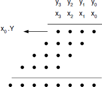
Figure 12.16 Binary products dot scheme.
12.1.6 Per Gelosia Multiplication Arrays
12.1.6.1 Introduction
Whenever base B is greater than 2, partial products appear less straightforward than what is involved in binary products (straight AND operation). Moreover, base-B elementary products generate carries. This basic difference between respective multiplication processes is illustrated in Figures 12.16 and 12.17, where dot schemes are presented without loss of generality for 4-digit multiplication.
Figure 12.16 displays the classical shift and add scheme, where each line i stands for the binary expression of xi.Y. The problem is reduced to a multioperand sum process. In Figure 12.17, the dot diagram suggests that xi.Y is not explicitly completed, xi.Y is presented as a subdiagram, where each xi.yj appears as a shifted double dot dealing with carries generated through partial products generation. Per Gelosia technique doesn't compute xi.Y, allowing a parallel treatment of all partial products xi.yj. Each 2-digit partial product is then part of a multioperand base-B adding scheme ([DAV1977]).

Figure 12.17 Base-B products dot scheme.
12.1.6.2 Adding Tree for Base-B Partial Products
The adding stage dot diagram of Figure 12.17, generalized to n-bit × n-bit B-ary multiplication, is represented in Figure 12.18. The maximum depth of the tree displayed in Figure 12.18 is 2.n − 1; therefore, (m, k) B-ary counters can be fruitfully used to reduce the tree. An example is given hereafter for n = 4.
Example 12.9 We present a reduction tree for 4-digit × 4-digit multiplication in base 6. (3, 2), (5, 2), and (7, 2) counters are needed to proceed to a 2-operand reduction in one stage. Then a B-ary ripple-carry adder can be used (Figure 12.19).
Observe that, as far as 2.n − 1 doesn't exceed B + 1, (m, 2)-counters can be used to get the two summands within one reduction stage (sufficient condition). Whenever n increases with respect to B, a k-operand reduction can be made with (m, k)-counters, with k > 2, and/or more reduction stages.
The 4-digit x 4-digit multiplication circuit is shown in Figure 12.20, where partial products Xi.yj are quoted as (Pij1, Pij0). With this indexing rule, each column L of the adding tree is characterized by:
![]()
L being the rank of the column.

Figure 12.18 Adding stage dot diagram for n-digit base-B multiplication.

Figure 12.19 (4 × 4)-digit dot scheme.
Comment 12.2 According to Section 11.1.12 of Chapter 11, multioperand addition (m n-bit operands), using a carry-save reduction tree followed by a fast (logarithmic delay) adder, has an overall computation time given by T(m,n) = O(log m.n). Considering that the partial products can be performed in parallel, this order of magnitude can be assumed for implementations of m-digit by n-digit multiplication based on this technique.

Figure 12.20 Counters and adder stage.
12.1.7 FPGA Implementation of Multipliers
In order to take advantage of the Virtex-family slice structure, relation (5.4) can be slightly modified as follows (B = 2, n even):
Every term of the preceding sum can be computed with an (m + 1)-cell iterative circuit whose basic ij-cell (computation of (2.xi+1 + xi).Y) is shown in Figure 12.21.
The look-up table computes
![]()
so that
![]()
where cin = cj and cout = cj+1.
Thus (m + 1).n/2 ij-cells are needed: i = 2k, k ∈ [0,(n − 2)/2]; j ∈ [0, m]; y−1 = ym = 0.
It remains to compute the sum (12.7) of the so obtained (and previously shifted) n/2 terms. Figure 12.22 displays the complete circuit for n = 6, m = 4. As before, inputs x and y are not represented. Observe that the iterative line i actually computes a 2-operand sum. The look-up tables recursively compute the values of the propagate function as defined in Chapter 4. Figure 12.22 corresponds to ripple-carry adders implementation; nevertheless, each option remains open to the designer. The carry-skip technique (Chapter 11, Section 11.1.10.2) is particularly well suited for high-speed adders on FPGA ([BIO2003]). In Figure 12.22, a carry-save reduction tree, using full adders, provides two operands processed by a ripple-carry adder. This last adding step could also be left open to the designer.
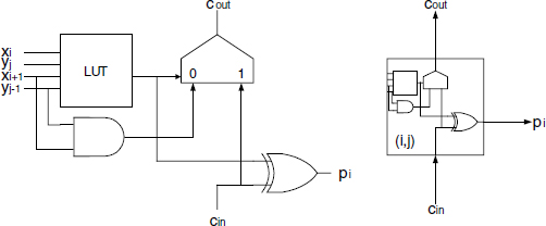
Figure 12.21 Slice configuration.

Figure 12.22 A 4-bit by 6-bit multiplier on FPGA.
The cost in terms of (i, j)-cells of this implementation is given by
![]()
The cost of the carry-save reduction, with full adders, is asymptotically equal to
![]()
while the cost of the 2-operand adder is linear with n + m.
The delays mainly depend on the type of adders and elementary counter cells selected for carry-save reduction. This delay may be expressed as
![]()
where Textended-adder (m) stands for the time delay involved in the iterative circuit computing (2.xi+1 + xi).Y, Tadder stands for the delay of the final adding stage, and Tcarry-save represents the carry-save reduction tree delay.
Observe that Textended-adder (m) depends only on m, because functions (2.xi+1 + xi).Y are computed in parallel. Whenever n < m, the number of operands to be added decreases but the operand length increases, so that the final adding stage will be accordingly longer.