
Chapter ID-1
Dye-Sensitized Photoelectrochemical Cells
Chapter Outline
2.1. Levels of Energy and Potential
2.4. The Semiconductor--Electrolyte Junction
2.5. Light-Induced Charge Separation
2.7. Basic Operational Principles of Photoelectrochemical Cells
3.1. Overview of Current Status and Operational Principles
3.2. Overview of the Different Electron-Transfer Processes
3.2.1. Reactions 1 and 2: Electron Injection and Excited State Decay
3.2.2. Reaction 3: Regeneration of the Oxidized Dyes
3.2.3. Reaction 4: Electron Transport Through the Mesoporous Oxide Film
3.2.4. Reaction 5 and 6: Recombination of Electrons in the Semiconductor with Oxidized Dyes or Electrolyte Species
3.2.5. Reaction 7: Transport of the Redox Mediator and Reactions at the Counterelectrode
3.3. Characterization of DSC Devices
3.3.1. Efficiency Measurements
3.3.2. External and Internal Quantum Efficiencies
3.3.4. The Stark Effect in DSC
3.4. Development of Material Components and Devices
1 Introduction
The magnitude of the change required in the global energy system will be huge. The challenge is to find a way forward that simultaneously addresses issues of energy supply and saving, climate change, security, equity, and economics. The mean global energy consumption rate was 13 terawatt (TW) in the year 2000. Assuming a kind of “business-as-usual” scenario with rather optimistic but reasonable assumptions of population growth and energy consumption, the projection is that the global energy demand in 2050 will at least be double. Solar energy will play a pivotal role in the paradigm shift that is needed for energy supply. After fusion, solar energy has the largest potential to satisfy future global needs for renewable energy sources. From the 1.7×10⁵ TW of solar energy that strikes Earth’s surface, a practical terrestrial global solar potential value is estimated to be about 600 TW. Thus, using 10% efficient solar farms, about 60 TW of power could be supplied. The umbrella of solar-energy conversion encompasses solar thermal, solar fuels, solar-to-electricity (photovoltaic, PV) technology, and the great many subcategories below those. Photovoltaics, or solar cells, are fast growing both with regards to industrialization and research. Globally, the total PV installation is around 40 gigawatt (GW), and an annual growth rate of 45% has been experienced over recent years. Solar cell technologies can be divided into three generations. The first is established technology such as crystalline silicon. The second includes the emerging thin-film technologies that have just entered the market, while the third generation covers future technologies that are not yet commercialized. A link for PV updates is www.solarbuzz.com, and our own contribution for a review of PV technologies with special emphasis on the materials science aspects is reference [1].
When comparing different photovoltaic technologies, a figure of merit is the production cost per peak watt of solar electricity produced. For so-called second-generation thin-film solar cells, production costs down to and even below $1/Wpeak are reported. To be competitive for large-scale electricity production, new PV technologies thus need to aim at production costs below $0.5/Wpeak. To give an example, this means a cost of 70 $/m2 at a module efficiency of 14%. The dye-sensitized solar cell (DSC) is a molecular solar cell technology that has the potential to achieve production costs below $0.5/Wpeak.
DSC is based on molecular- and nanometre-scale components. Record cell efficiencies of 12%, promising stability data and energy-efficient production methods, have been accomplished. In the present table of record solar cell efficiencies [2], in which the solar cell area must be at least 1 cm2, the record is held by the Sharp company in Japan at 10.4 ± 0.3% [3]. The record for a DSC module is 9.2% achieved by Sony, Japan [4]. As selling points for the DSC technology, the prospect of low-cost investments and fabrication and short energy-payback time (<1 year) are key features. DSCs offer the possibilities to design solar cells with a large flexibility in shape, colour, and transparency. Integration into different products opens up new commercial opportunities for niche applications. Ultimately, the comparison of different energy sources is based on the production cost per kWh—i.e., the cost in relation to energy production. For DSC technology, it is advantageous to compare energy cost rather than cost per peak watt. DSCs perform relatively better compared with other solar cell technologies under diffuse light conditions and at higher temperatures.
DSC research groups have been established around the world with the most active groups in Europe, Japan, Korea, China, and Australia. The field is growing fast, which can be illustrated by the fact that about two or three research articles are being published every day. From a fundamental research point of view, we can conclude that the physical chemistry of several of the basic operations in the DSC device remain far from fully understood. For specific model and reference systems and controlled conditions, there is a rather detailed description in terms of energetics and kinetics. It is, however, still not possible to predict accurately how a small change to the system—e.g., replacing one component or changing the electrolyte composition—will affect DSC performance. With time, the chemical complexity of DSCs has become clear, and the main challenge for future research is to understand and master this complexity, in particular at the oxide–dye–electrolyte interface. It is noteworthy that such a fundamental effect as the Stark shift of the dye molecules at the interface took more than 15 years to identify and describe. This was independently made by ourselves [5] and Meyer et al. [6], USA. A challenging but realizable goal for the present DSC technology is to achieve efficiencies above 15%. We have for many years known where the main losses in the state-of-the-art DSC device are—that is, the potential drop in the regeneration process and the recombination loss between electrons in the TiO2 and acceptor species in the electrolyte. With our breakthrough of using one-electron transfer redox systems such as co-complexes, in combination with a dye, which efficiently prevents the recombination loss, we may now have found the path to increase the efficiency significantly [7]. With the recent world record of 12.3 by Grätzel and co-workers [8] using co-complexes, the main direction of the research field is now to explore this path.
The industrial interest in DSCs is strong with large multinational companies such as BASF and Tata Steel in Europe and Toyota, Sharp, Panasonic, Sony, Fujikura, and Samsung in Asia. These companies present encouraging results, in particular with regard to upscaling with world record minimodule efficiencies above 9% (Sony and Fujikura). In this context, we note that world record efficiencies are not the same as stable efficiencies obtained after durability tests. Reported stable module efficiencies vary significantly in the literature and are difficult to judge. Best values in the literature are about 5%, although presentations at conferences report better results. Several companies are dedicated to setting up manufacturing pilot lines. G24i is a company based in Cardiff, Wales, that focuses on consumer electronics. On its Web site (www.g24i.com), such niche products are now for sale. Companies that sell material components, equipment, and consultancy services have increased and are growing.
The structure of this chapter basically follows the paper by McEvoy in the first edition of Practical Handbook of Photovoltaics: Fundamentals and Applications [9]. Our aim is to provide the reader with a general description of photoelectrochemical cells with a specific focus on DSCs. There are several recent reviews on DSCs, and the reader is referred to these papers for further information [10–22]. Instead of trying to add another review article to the field, we want to make this chapter more of a handbook. We present the general concepts and principles of PEC and put more emphasis on different types of characterization methods for DSC devices rather than provide detailed overviews of, for example, materials development. This also means that the reference list is more of a general summary of the field, including mainly books, review articles, and some original papers.
2 Photoelectrochemical Cells
The photovoltaic effect was first observed by A.-E. Becquerel almost 200 years ago [23] when he illuminated a thin layer of silver chloride coated on a sheet of Pt immersed in an electrolytic solution and connected to a counterelectrode. The Becquerel device would at present be classified as a photoelectrochemical (PEC) cell, see, for example, reference [9]. The contact of the semiconductor with the electrolyte, in which the conduction mechanism is the mobility of ions rather than of electrons or holes, forms a photoactive junction functionally equivalent to those later discovered for solid-state photovoltaic devices. Unlike their solid-state counterparts, however, semiconductor–liquid junctions are versatile in that solar energy can be used to drive chemical reactions—for example, for the production of chemical fuels and self-cleaning and anti-fogging surfaces. For an interesting and recent review on the origins of photoelectrochemistry, see reference [24].
The first boom of photoelectrochemistry came with the famous 1972 paper of Fujishima and Honda, who reported the use of a TiO2 photoanode in an electrochemical cell to split water into H2 and O2 [25]. As pointed out by Rajeshwar [24], perhaps the first instance of the use of a light-responsive electrode for the photo-assisted decomposition of water is the 1960 paper ‘Decomposition of Water by Light’ [26]. The promising results of PEC cells as solar-energy converters together with the 1973 oil crisis triggered a dramatic growth of research in this area. From an industrial point of view, the biggest success so far of the Fujishima–Honda paper was probably the development of photocatalytic TiO2 systems for environmental remediation, self-cleaning materials, and antifogging surfaces [24,27,28]. For solar-energy conversion, the intense activities on PEC systems from the mid-1970s to the mid-1980s was followed by a considerable slowing down of the progress [24]. The second boom of photoelectrochemistry for solar-energy conversion occurred in the early 1990s starting with the seminal paper by O’Regan and Grätzel in 1991 [29]. The very unexpected finding that a high-surface-area electrode could be used to dramatically increase the performance of dye-sensitized photoelectrochemical cells caused a paradigm shift in the understanding of how an efficient solar cell can be prepared and operate. The principle of dye-sensitized solar cells has also become a part of the core chemistry and energy science teaching and research. Textbooks have sections or chapters dealing with DSC [30,31]. Laboratory kits have been developed for educational purposes making use of dyes from all possible natural sources such as blackberries, spinach, blueberries, tea, and wine. Not only photoelectrochemistry but also energy science, photochemistry, materials science, and transition metal coordination chemistry have significantly benefitted from DSC research.
The basic structure of a PEC cell is a working electrode (semiconductor), an electrolyte, and a counterelectrode (normally a metallic material with a low overpotential for reduction–oxidation of the electrolyte). The heart of the device is the semiconductor–electrolyte interface (SEI) of the working electrode. In the following, we go through the basic features of this interface, starting with the individual components followed by the description of the SEI and finishing with the phenomenon of dye sensitization.
2.1 Levels of Energy and Potential
The semiconductor–electrolyte junction is an ‘interface’ between physics and chemistry. In solid-state physics and electrochemistry, one normally uses the energy scale with vacuum as reference for the former and the potential scale with the standard hydrogen electrode (SHE) or normal hydrogen electrode (NHE) as reference for the latter. The electrochemical potential of electrons in a semiconductor is normally referred to as the Fermi level, EF, and in an electrolyte solution it is often referred to as the redox potential, ![]() in energy scale and
in energy scale and ![]() in potential scale. At equilibrium, the electrochemical potentials (or the Fermi levels) of the semiconductor and electrolyte will be equal. For most purposes in electrochemistry, it is sufficient to reference the redox potentials to the NHE (or any other more practical reference system), but it is sometimes of interest to have an estimate of the absolute potential (i.e., versus the potential of a free electron in vacuum). For example, it may be of interest to estimate relative potentials of semiconductors, redox electrolytes, and solid hole conductors in solid-state DSC based on their work functions. Taking a redox system dissolved in an electrolyte as an example, the absolute energy of a system is shifted against the conventional scale by the free energy Eref, according to
in potential scale. At equilibrium, the electrochemical potentials (or the Fermi levels) of the semiconductor and electrolyte will be equal. For most purposes in electrochemistry, it is sufficient to reference the redox potentials to the NHE (or any other more practical reference system), but it is sometimes of interest to have an estimate of the absolute potential (i.e., versus the potential of a free electron in vacuum). For example, it may be of interest to estimate relative potentials of semiconductors, redox electrolytes, and solid hole conductors in solid-state DSC based on their work functions. Taking a redox system dissolved in an electrolyte as an example, the absolute energy of a system is shifted against the conventional scale by the free energy Eref, according to
![]() (1)
(1)
For the NHE, ![]() is estimated to be −4.6±0.1 eV63. With this value, the standard potentials of other redox couples can be expressed on the absolute scale.
is estimated to be −4.6±0.1 eV63. With this value, the standard potentials of other redox couples can be expressed on the absolute scale.
2.2 The Semiconductor
In nondegenerate semiconductors, the equilibrium Fermi level is given by
![]() (2)
(2)
where Ec is the energy at the conduction band edge, kBT is the thermal energy, nc is the density of conduction band electrons, and Nc is the effective density of conduction band states. With respect to vacuum, Ec is given by the electron affinity EA, as shown in Figure 1. The ionization energy, I, in the same figure determines the position of the valence band, EV, whereas the distance between the vacuum level and the equilibrium Fermi level is the work function, ![]() . Thus, the positions of the energy bands can be predicted from electron-affinity values.
. Thus, the positions of the energy bands can be predicted from electron-affinity values.

FIGURE 1 Positions of energy bands for a semiconductor with respect to vacuum level.
However, these values are very sensitive to the environment, and measurements of absolute and relative energies in vacuum must be carefully interpreted and analyzed in terms of their relevance to DSCs. In the field of semiconductor electrochemistry, the standard approach of determining the so-called flatband potential of a semiconductor, Vfb, which estimates the work function of the semiconductor in contact with the specific electrolyte, is Mott-Schottky analysis of capacitance data [32]. This approach is based on the potential-dependent capacitance of a depletion layer at the semiconductor surface. For a DSC, such behaviour is not expected to be observed for the ~20-nm anatase nanocrystals that are expected to be fully depleted [10,14]. Instead, cyclic voltammetry and spectroelectrochemical procedures have been used to estimate Ec. These methods also give information of the density of states (DOS) of the semiconductor.
For a recent review on the measurements of Ec, and the density of states in mesoporous TiO2 films, see reference [14]. Fitzmaurice has reviewed the first spectroelectrochemical measurements of Ec for transparent mesoporous TiO2 electrodes [33]. Using an accumulation-layer model to describe the potential distribution within the TiO2 nanoparticle at negative potentials [34], and assuming that Ec remains fixed as the Fermi level is raised into accumulation conditions, Ec values in organic and aqueous electrolytes were estimated. At present there is an extensive compilation of data that shows that Ec is not that well defined. Many electrochemical and spectroelectrochemical studies indicate that mesoporous TiO2 films possess a tailing of the DOS (trap states) rather than an abrupt onset from an ideal Ec. Nevertheless, the Ec values estimated in the early work by Fitzmaurice and co-workers are still used today, at least qualitatively, to discuss, for example, the energy-level matching between the conduction band edge of the oxide and the excited state of the dye.
The position of the conduction band edge depends on the surface charge (dipole potential). The pH dependence of Ec for mesoporous TiO2 films in aqueous solutions follows a Nernstian behaviour with a shift of 59 mV/pH unit due to protonation–deprotonation of surface titanol groups on TiO2 (see references [14,34]). In nonaqueous solutions, Ec can be widely tuned by the presence of positive ions, cations. This effect is greatest with cations possessing a large charge-to-radius ratio. For example, Ec has been reported to be –1.0 V vs. SCE in 0.1 M LiClO4 acetonitrile electrolyte and ~–2.0 V when Li+ was replaced by a large cation, tert-butyl ammonium. The large variation of Ec with different ‘potential-determining’ ions can be explained by cation-coupled reduction potentials for TiO2 acceptor states, due to surface adsorption or insertion into the anatase lattice [14]. This cation-dependent shift in Ec is used to promote photo-induced electron injection from the surface-bound sensitizer. For this to occur, Ec must be at a lower energy than the excited state of the sensitizer, S+/S∗. In contrast, one would like Ec to be at as high energy as possible to achieve a high photovoltage. Thus, there is a compromise for the position of Ec in order to attain an efficient electron injection while maintaining a high photovoltage. Additives in the electrolyte are normally used to fine-tune the energy-level matching of Ec and S+/S∗. The effect of the additive—most often 4-tert-butylpyridine (tBP) is used—can be studied by measuring the relative shifts of Ec, depending on surface charge, and by measuring the electron lifetime. The shift of Ec is measured by charge-extraction methods and electron lifetime measurements as described in the toolbox section.
2.3 The Electrolyte
The electrochemical potential of electrons, or the Fermi level, for a one-electron redox couple is given by the Nernst equation and can be written as
![]() (3)
(3)
where cox and cred are the concentrations of the oxidized and reduced species of the redox system. Besides the Fermi energy, we also need a description of the energy states being empty or occupied by electrons. The electronic energies of a redox system are shown in Figure 2 and are based on the model developed by Gerischer [32,35–37].

FIGURE 2 (a) Electron energies of a redox system using vacuum as a reference level. ![]() ,
, ![]() ,
, ![]() . (b) Corresponding distribution functions.
. (b) Corresponding distribution functions.
In this energy scale, Ered0 corresponds to the energy position of occupied electron states and Eox0 to the empty states. They differ from the Fermi level EF,redox0 by the so-called reorganization energy, λ. The reorganization energy is the energy involved in the relaxation process of the solvation shell around the reduced species following transfer of an electron to the vacuum level. For the reverse process—i.e., electron transfer from vacuum to the oxidized species—there is an analogous relaxation process. It is normally assumed that λ is equal for both processes. The electron states of a redox system are not discrete energy levels but are distributed over a certain energy range due to fluctuations in the solvation shell surrounding the molecule. This is indicated by the distribution of energy states around E0red and Eox0 (Figure 2b). Dred is the density of occupied states (in relative units) represented by the reduced component of the redox system and Dox the density of empty states represented by the oxidized component. Assuming a harmonic oscillation of the solvation shell, the distribution curves, Dred and Dox, are described by Gaussian functions:
![]() (4)
(4)
![]() (5)
(5)
Dred0 and Dox0 are normalizing factors such that ![]() . The half-width of the distribution curves is given by
. The half-width of the distribution curves is given by
![]() (6)
(6)
Accordingly, the widths of the distribution function depend on the reorganization energy, which is of importance for the kinetics of electron-transfer processes at the oxide–dye–electrolyte interface. Typical values of λ are in the range from a few 10ths of an eV up to 2 eV. In Figure 2b, the concentrations of reduced and oxidized species are equal (Dred = Dox). Changing the concentration ratio varies the redox potential (EF,redox0), according to the Nernst equation.
2.4 The Semiconductor--Electrolyte Junction
If a semiconductor is immersed in the electrolyte, chemical equilibrium will be established—i.e., the Fermi levels of the semiconductor and the electrolyte will adjust to each other and
![]() (7)
(7)
where q is the elementary charge and Vredox the electrochemical (redox) potential of the electrolyte. From now on, we limit the discussion to n-type doped semiconductors keeping in mind that the inverse but analogous situation occurs with p-type semiconductors. For an n-type semiconductor with the initial Fermi level higher than the redox potential, the equilibration of EF and EF, redox occurs by transfer of electrons from the semiconductor to the electrolyte. This will produce an electrical field in the solid—i.e., the so-called space charge layer (also referred to as the depletion layer since the region is depleted of majority carries) (see Figure 3).
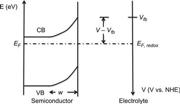
FIGURE 3 Energy-versus-distance diagram for an n-type semiconductor–liquid junction in equilibrium. For an n-type semiconductor, the space charge region, w, is positively charged due to depletion of conduction band electrons.
For an n-type semiconductor the space charge layer is positive. The electric field is represented by curvature of the conduction and the valence bands (band bending) and indicate the direction that the free carriers will migrate in the field. The width of the space charge layer was derived by Gärtner [38] to be
![]() (8)
(8)
where ε is the relative dielectric constant, ε0 the permittivity of free space, ND the donor concentration (or dopant density), and Vfb and V the electrostatic potentials of the semiconductor surface and the bulk, respectively. Thus, V—Vfb gives the band bending. While the space charge layer normally extends from a few nanometres to micrometres, the main part of the potential drops takes place in the solution within a few Ångströms of the surface in the so-called Helmholtz layer. This is particularly the case in solutions with high ionic strengths.
For a semiconductor, the space charge layer formed gives rise to a capacitance CSC in this region, which is usually much smaller than that of the adjacent Helmholtz layer in the electrolyte, CH. Since the total capacity is given by
![]() (9)
(9)
it follows that 1/C≈1/CSC. Thus, any variation in an externally applied voltage, V, often changes only the potential drop within the semiconductor—i.e., the Fermi level in the semiconductor—and so the band bending is changed. The energy (or potential) difference between the conduction band edge position at the semiconductor surface and Fermi level of the electrolyte is therefore not affected by the external voltage. The flatband potential, Vfb, is the potential at which the semiconductor bands are flat (zero space charge), and is measured with respect to a reference electrode with a well-defined electrode potential.
The above-described situation is different in a colloidal semiconductor or in a nanocrystalline network. The potential distribution in a spherical semiconductor particle has been derived by semiconductor nanoparticles, the total potential drop within the semiconductor becomes
![]() (10)
(10)
where r0 is the radius of the particle and LD = (εε0kT/2q2ND)0.5 is the Debye length, which depends on the number of ionized dopant molecules per cubic centimetre, ND. From this equation, it is apparent that the electrical field in semiconductor nanoparticles is usually small and that high dopant levels are required to produce a significant potential difference between the surface and the center of the particle. For example, in order to obtain a 50 mV potential drop in a TiO2 nanoparticle with ro = 6 nm, a concentration of 5×1019 cm−3 of ionized donor impurities is necessary. Undoped TiO2 nanoparticles have a much smaller carrier concentration and the band bending within the particles is therefore negligibly small.
This chapter focuses on dye-sensitized solar cells, which are based on a mesoporous semiconductor oxide film. When the dye-sensitized mesoporous solar cell was first presented, perhaps the most puzzling phenomenon was the highly efficient charge transport through the nanocrystalline TiO2 layer. Early on it was realized that the mesoporous electrodes were very much different compared to their compact analogues described above because (1) the inherent conductivity of the film is very low, (2) the small size of the individual colloidal particles does not support a built-in electrical field, and (3) the oxide particles and the electrolyte-containing pores form interpenetrating networks whose phase boundaries produce a junction of huge contact area. These films are thus best viewed as an ensemble of individual particles through which electrons can percolate by hopping from one crystallite to the next. Charge transport in mesoporous systems is still under keen debate today [21,39–41] and will be described in Section 3.2.3. Common characteristics in the operations of mesoporous oxide electrodes are the filling of trap states and that the charge-separation process after photoexcitation is mainly governed by the kinetics at the SEI.
The effect of an external field in a mesoporous semiconductor film is then different compared to the discussion above for a doped compact semiconductor in which the applied potential changed the band bending of the semiconductor. Since there is no macroscopic space charge layer formed in a mesoporous electrode, the applied potential will change the Fermi level at the back contact (conducting substrate–mesoporous oxide interface) throughout the mesoporous film with the result of a different electron concentration of the electrode compared to zero bias. The term flatband potential is therefore not appropriate for a mesoporous electrode. The term position of the conduction band edge, Ec, is then used for conventional DSC systems.
2.5 Light-Induced Charge Separation
The depletion layer at the interface between a compact semiconductor and a liquid medium plays an important role in light-induced charge separation. The local electrostatic field present in the space charge layer serves to separate the electron–hole pairs generated by illumination of the semiconductor. For n-type materials, the direction of the field is such that holes migrate to the surface where they undergo a chemical reaction, while the electrons drift through the bulk to the back contact of the semiconductor and subsequently through the external circuit to the counterelectrode. Charge carriers which are photogenerated in the field-free space of the semiconductor can also contribute to the photocurrent. In solids with low defect concentration, the lifetime of the electron–hole pairs is long enough to allow for some of the minority carriers to diffuse to the depletion layer before they undergo recombination.
In the case of semiconductor nanoparticles, the band bending is small and charge separation occurs via diffusion. The absorption of light leads to the generation of electron–hole pairs in the particle, which are oriented in a spatially random fashion along the optical path. These charge carriers subsequently recombine or diffuse to the surface where they undergo chemical reactions with suitable solutes or catalysts deposited on the surface of the particles. Since in nanoparticles the diffusion of charge carriers from the interior to the particle surface can occur more rapidly than their recombination, it is feasible to obtain quantum yields for photoredox processes approaching unity. Whether such high efficiencies can really be achieved depends on the rapid removal of at least one type of charge carrier—i.e., either electrons or holes—upon their arrival at the interface. This underlines the important role played by the interfacial charge-transfer kinetics.
The charge-separation process in mesoporous electrodes was measured independently for mesoporous TiO2 films [42] and electrodeposited CdS and chemically deposited CdSe [43]. High quantum yields were measured in all cases. By illuminating the mesoporous film both through the electrolyte and through the transparent conducting oxide (TCO) substrate, the dependence of the quantum yield as a function of depth in the semiconductor film could be monitored. From these measurements, a qualitative model to describe the photocurrent generation in nanocrystalline films was presented. The electrolyte penetrates the whole mesoporous film up to the surface of the back contact, and a semiconductor–electrolyte junction occurs thus at each nanocrystal, much like a normal nanoparticle system. During illumination, light absorption in any individual nanoparticle will generate an electron–hole pair. Assuming that the kinetics of charge transfer to the electrolyte is much faster for one of the charges (holes for TiO2) than for the recombination processes, the other charge (electrons) can create a gradient in the electrochemical potential between the particle and the back contact. In this gradient, the electrons (for TiO2) can be transported through the interconnected colloidal particles to the back contact, where they are withdrawn as a current. The charge separation in a mesoporous semiconductor electrode therefore does not need to depend on a built-in electric field but is mainly determined by kinetics at the SEI. The creation of the light-induced electrochemical potential for the electrons in TiO2 also explains the building up of a photovoltage. Early on in DSC research it was concluded that charge transport in mesoporous films is dominated by diffusion of the charge carriers [44].
2.6 Dye Sensitization
The history of dye-sensitized photoelectrochemical cells goes back to the early days of colour photography. For further insights into this interesting parallel between sensitization in photography and photoelectrochemistry, readers are referred to references [9,12,45]. In 1873, Vogel, professor of “photochemistry, spectroscopy and photography” in Berlin, established empirically that silver halide emulsions could be sensitized to red and even infrared light by suitably chosen dyes [46]. The concept of dye enhancement was carried over already by 1887 from photography to the photoelectric effect by Moser [47] using the dye erythrosine, again on silver halide electrodes. That the same dyes were particularly effective for both processes was recognized among others by Namba and Hishiki [48] at the 1964 International Conference on Photosensitization in Solids in Chicago, a seminal event in the history of dyes in the photosciences. It was also recognized there that the dye should be adsorbed on the semiconductor surface in a closely packed monolayer for maximum sensitization efficiency [49]. On that occasion, the theoretical understanding of the processes was clarified, since until then it was still disputed whether the mechanism was a charge transfer or an Auger-like energy-coupling process. With the subsequent work of Gerischer and Tributsch [50,51] on ZnO, there could be no further doubt about the mechanism, and it was evident that the process involved the excitation of the dye from its charge-neutral ground state to an excited state by the absorption of the energy of a photon followed by a charge transfer from the excited dye to the semiconductor.
Excitation of a sensitizer dye molecule, S, for example by the absorption of the energy of a photon, can promote an electron from the highest occupied molecular orbital (HOMO) to the lowest unoccupied molecular level (LUMO). Therefore, as far as absorption of light is concerned, the HOMO–LUMO gap of a molecule is fully analogous to the band gap of a semiconductor. It defines the response to incident light and consequently the optical absorption spectrum. At the same time, the absolute energy level of the excited state of S, approximately the LUMO, can determine the energetics of the permitted relaxation processes of the excited molecule. When it lies above the conduction band edge of a semiconductor substrate, relaxation may take the form of emission of an electron from the dye into the semiconductor, leaving that molecule in a positively charged oxidized state. The Fermi level of the oxidation potential of S is E0F,redox(S/S+). An excited sensitizer, S∗, is more easily reduced or oxidized, because of the excitation energy ΔE∗ stored in the molecule. The Fermi levels of excited molecules, E∗F,redox(S∗/S+), can be estimated by adding ΔE∗ from the redox energy level of the molecule in the ground state. The stored excitation energy ΔE∗ corresponds to the energy of the 0–0 transition between the lowest vibrational levels in the ground and excited states—that is, ΔE∗ = ΔE0−0. ΔE0−0 can be estimated by the photoluminescence (PL) onset or from the intersection of the absorption and PL spectra. If difficulties arise in measuring the PL spectrum, another way to estimate ΔE0−0 is from the absorption onset of the dyes adsorbed on the oxide at a certain percentage (e.g., 10%) of the full amplitude at the absorption maximum.
Introducing the corresponding distribution functions of the occupied and empty states for the most relevant reactions in a photoelectrochemical cell, we arrive at a so-called Gerischer diagram for an excited-state electron injection from surface-bound sensitizers into the density of states of a TiO2 film (Figure 4). In Figure 4, the distribution functions of the empty and occupied states for the ground state and excited state are drawn with equal areas, indicating that the concentrations of the different species are the same. Differences in concentration will lead to different Fermi levels, E0F,redox(S/S+) and E∗F,redox(S∗/S+), and thus, different driving forces for electron injection and for regeneration of the oxidized dyes by the electrolyte. The actual concentrations of the different species indicated in Figure 4 will depend on several factors such as the Fermi levels of the semiconductor and electrolyte, dye loading, extinction coefficients, and light intensity.
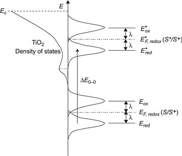
FIGURE 4 Gerischer diagram of DSC with iodide–triiodide electrolyte. The level of the unstable reaction intermediate didiodide (I2−) is indicated.
(Adapted from reference [14] and reproduced by permission of the Royal Society of Chemistry; and reference [35], copyright 1985, with permission from Elsevier.)
2.7 Basic Operational Principles of Photoelectrochemical Cells
DSC is an example of a PEC cell that converts solar energy to electricity. The basic operational principles of such a device are described in Section 3.1. Since a PEC can be integrated into an electrolytic cell, it is also an option that electrochemistry can give rise to a photoelectrolytic or a photosynthetic effect converting solar energy to chemistry. Figure 5 is an example of an energy-level diagram for photoelectrolysis [32,35] in which water is split into its elements as reported by Fujishima and Honda [25]. In Figure 5, light is absorbed by an n-type semiconductor electrode in contact with a water-based electrolyte.

FIGURE 5 Energy-level diagram for photoelectrolysis in which water is split into its elements.
The counterelectrode on the right-hand side of the figure is a metal, and the whole configuration is similar to a photoelectrochemical photovoltaic cell. The two electrodes are short-circuited by an external wire. In the case of an n-type semiconductor electrode, the holes created by light excitation must react with H2O, resulting in O2 formation, whereas at the counterelectrode H2 is produced. The electrolyte can be described by two redox potentials (Fermi levels)—E0F,redox(H2O/H2) and E0F,redox(H2O/O2)—that differ by 1.23 eV. The two reactions can obviously only occur if the band gap is >1.23 eV, the conduction band in energy being above E0F,redox(H2O/H2) and the valence band below (positive) E0F,redox(H2O/O2). Since multielectronic steps are involved in the reduction of and oxidation of H2O, certain overvoltages occur for the individual processes that lead to losses. In general, it can be stated that it is usually easy to produce hydrogen with n-type semiconductor electrodes; the real problem is the oxidation of H2O. Much research is at present taking place and being launched worldwide to address this “holy grail” of photoelectrochemistry, also with the use of molecular systems such as ruthenium complexes for light absorption and oxygen evolution [52,53].
3 Dye-Sensitized Solar Cells
Attempts to develop dye-sensitized photoelectrochemical cells had been made before [12,45,54,55] the breakthrough of O’Regan and Grätzel in 1991 [29]. The basic problem was the belief that only smooth semiconductor surfaces could be used. The light-harvesting efficiency (LHE) for a monomolecular layer of dye sensitizer is far less than 1% of the AM 1.5 spectrum. Attempts to harvest more light by using multilayers of dyes were in general unsuccessful. Indications of the possibilities to increase the roughness of the semiconductor surface so that a larger number of dyes could be adsorbed directly to the surface and simultaneously be in direct contact with a redox electrolyte had also been reported before 1991. For example, Matsumura et al. [56] and Alonso et al. [57] used sintered ZnO electrodes to increase the efficiency of sensitization by rose bengal and related dyes. But the conversion yields from solar light to electricity remained well below 1% for these systems. Grätzel, Augustynski, and co-workers presented results on dye-sensitized fractal-type TiO2 electrodes with high surface area in 1985 [58]. For DSC, there was thus an order-of-magnitude increase when O’Regan and Grätzel in 1991 reported efficiencies of 7–8% [29]. With regards to stability, a turnover number of 5×10⁶ was measured for the ruthenium-complex sensitizer. This was followed up by the introduction of the famous N3 dye, giving efficiencies around 10% [59]. For more than a decade, the ruthenium complex N3, Ru(Lbip)2 (NCS)2 with Lbip being a dicarboxylated bipyridyl ligand, its salt analogue N719, and the so-called black dye RuLter(NCS)3 with L being a ter-pyridyl ligand, were state-of-the art sensitizers. Recently developed Ru complexes such as C101 show now higher performances both in terms of efficiency and stability [20,60]. The molecular structures of N3, the black dye, and C101 are shown in Figure 6.
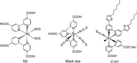
FIGURE 6 Molecular structures of N3, the black dye, and C101.
3.1 Overview of Current Status and Operational Principles
Since the initial work in the beginning of the 1990s, a wealth of DSC components and configurations have been developed. At present, several thousands of dyes have been investigated. Fewer, but certainly hundreds of electrolyte systems and mesoporous films with different morphologies and compositions have been studied and optimized. For DSCs at present, in the official table of world record efficiencies for solar cells, the record is held by the Sharp company in Japan at 10.4±0.3% [61]. A criterion to qualify for these tables is that the solar cell area is at least 1 cm2. For smaller cells, conversion efficiencies above 12% have been reached using the so-called C101 sensitizer as the sensitizer and with Co-complex based electrolytes [8], see Section 3.4.3.
A schematic of the interior of a DSC showing the principle of how the device operates is shown in Figure 7.

FIGURE 7 A schematic of the interior of a DSC showing the principle of how the device operates.
The typical configuration is as follows. At the heart of the device is the mesoporous oxide layer composed of a network of TiO2 nanoparticles, which have been sintered together to establish electronic conduction. The layer is in the sintering step also deposited on a transparent conducting oxide (TCO) substrate forming an ohmic contact. Typically, the mesoporous film thickness is ca 10 μm and the nanoparticle size 10–30 nm in diameter; the porosity is 50–60%. The mesoporous layer is deposited on a transparent conducting oxide on a glass or plastic substrate. A typical scanning electron microscopy (SEM) image of a mesoporous TiO2 film is shown in Figure 8.

FIGURE 8 SEM picture of a typical mesoporous TiO2 film.
Attached to the surface of the nanocrystalline film is a monolayer of the charge-transfer dye. Photoexcitation of the latter results in the injection of an electron into the conduction band of the oxide leaving the dye in its oxidized state. The dye is restored to its ground state by electron transfer from the electrolyte, usually an organic solvent containing the iodide–tri-iodide redox system. The regeneration of the sensitizer by iodide inhibits the recapture of the conduction band electron by the oxidized dye. The I3− ions formed by oxidation of I− diffuse a short distance (<50 μm) through the electrolyte to the cathode, which is coated with a thin layer of platinum catalyst where the regenerative cycle is completed by electron transfer to reduce I3− to I−. For a DSC to be durable for more than 15 years outdoors, the required turnover number is 108, which is attained by the ruthenium complexes mentioned above.
The voltage generated under illumination corresponds to the difference between the electrochemical potential of the electron at the two contacts, which for DSCs is generally the difference between the Fermi level of the mesoporous TiO2 layer and the redox potential of the electrolyte. Overall, electric power is generated without permanent chemical transformation.
As mentioned earlier, a huge number of material components, dyes, mesoporous and nanostructured electrodes, electrolytes, and counterelectrodes have been synthesized and developed for DSC applications. The material component variations of a DSC device are therefore endless. It is important to keep in mind that the description above, and the one below in the next section, of the conventional DSC device with a mesoporous TiO2, a Ru-complex sensitizer, I−/I3− redox couple, and a platinized TCO counterelectrode is only valid for this particular combination of material components. As soon as one of these components is modified or completely replaced by another component, the picture has changed; energetics and kinetics are different and need to be determined for the particular system at hand. To generalize a result in DSC research is therefore difficult and can many times be misleading.
3.2 Overview of the Different Electron-Transfer Processes
The basic electron-transfer processes in a DSC, as well as the potentials for a state-of-the-art device based on the N3 dye adsorbed on TiO2 and I−/I3− as redox couple in the electrolyte, are shown in Figure 9. The corresponding kinetic data for the different electron-transfer processes taking place at the oxide–dye–electrolyte interface are summarized in Figure 10.
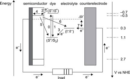
FIGURE 9 Simple energy-level diagram for a DSC. The basic electron-transfer processes are indicated by numbers (1–7). The potentials for a DSC based on the N3 dye, TiO2, and the I−/I3− redox couple are shown.
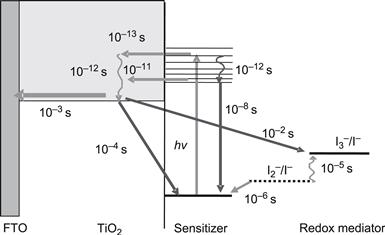
FIGURE 10 Summary of the kinetic data for the different electron-transfer processes depicted in Figure 9.
Besides the desired pathway of the electron-transfer processes (processes 2, 3, 4, and 7) described in Figure 9, the loss reactions 1, 5, and 6 are indicated. Reaction 2 is electron injection from the excited state of the dye to the semiconductor, 3 is regeneration of the oxidized dye by the electrolyte, 4 is electron transport through the mesoporous oxide layer, and 7 is the reduction of the electrolyte at the counterelectrode. Reaction 1 is direct recombination of the excited dye reflected by the excited state lifetime. Recombination reactions of injected electrons in the TiO2 with either oxidized dyes or with acceptors in the electrolyte are numbered 5 and 6, respectively. In principle, electron transfer to I3− can occur either at the interface between the nanocrystalline oxide and the electrolyte or at areas of the TCO contact that are exposed to the electrolyte. In practice, the second route can be suppressed by using a compact blocking layer of oxide deposited on the anode by spray pyrolysis [62,63]. Blocking layers are mandatory for DSCs that utilize one-electron redox systems or for cells using solid organic hole-conducting media [21].
3.2.1 Reactions 1 and 2: Electron Injection and Excited State Decay
One of the most astounding findings in DSC research is the ultrafast injection from the excited ruthenium complex in the TiO2 conduction band. Although the detailed mechanism of this injection process is still under debate, it is generally accepted that a fast, femtosecond (fs) component is observed for these types of sensitizers, directly attached to an oxide surface [64–67]. This would then be one of the fastest chemical processes known to date. There is a debate for a second, slower, injection component on the picosecond (ps) timescale. The reason for this could, on one hand, be due to an intersystem crossing of the excited dye from a singlet to a triplet state. The singlet state injects on the fs time scale whereas the slower component arises from the relaxation time of the singlet to triplet transition and from a lower driving force in energy between the triplet state and the conduction band of the TiO2 [67]. Another view of the slower component is that it is very sensitive to sample condition and originates from dye aggregates on the TiO2 surface [66]. For DSC device performance, the time scales of the injection process should be compared with direct recombination from the excited state of the dye to the ground state. This is given by the excited state lifetime of the dye, which for typical ruthenium complexes used in DSC, is 30–60 ns [11]. Thus, the injection process itself has not generally been considered to be a key factor limiting device performance. Koops et al. observed a much slower electron injection in a complete DSC device with a time constant of around 150 ps. This would then be slow enough for kinetic competition between electron injection and excited state decay of the dye, with potential implications for the overall DSC performance [68]. These results are debated since they are obtained with a single-photon counting technique that is a nondirect measurement of the injection process. A slower injection in the sub-ps time regime could be even more severe for organic dyes, for which the excited state decay time could be less than nanoseconds. Research on the electron injection process will thus continue to be an important topic in DSC research and needs to be extended to other classes of sensitizers beside the ruthenium complexes.
3.2.2 Reaction 3: Regeneration of the Oxidized Dyes
The interception of the oxidized by the electron donor, normally I−, is crucial for obtaining good collection yields and high cycle life of the sensitizer. For a turnover number (cycle life of the sensitizer in the DSSC device) above 108 (which is required for a DSC lifetime of >15 years in outdoor conditions), the lifetime of the oxidised dye must be longer than 100 s if the regeneration time is 1 μs [69]. This is achieved by the best performing ruthenium complexes such as C101.
A large number of sensitizers are efficiently regenerated by iodide, as follows from their good solar cell performance. Most of these sensitizers have oxidation potentials that are similar to or more positive than that of the standard N3 sensitizer Ru(Lbip)2(NCS)2 (V0redox = +1.10 V vs. NHE). Because the redox potential of the iodide–triiodide electrolyte with organic solvent is about +0.35 V versus NHE, the driving force ΔG0 for regeneration of N3 is 0.75 eV. It is of interest to estimate how much driving force is needed. Kuciauskas et al. [70] investigated regeneration kinetics of a series of Ru and Os complexes and found that Os(Lbip)2(NCS)2 with a ΔG0 = 0.52 eV is not (or is very slowly) regenerated by iodide, while Os(Lbip)2(CN)2 (ΔG0 = 0.82 eV) is regenerated. The black dye, RuLter(NCS)3, with ΔG0 = 0.60 eV, shows rapid regeneration [71]. Clifford et al. [72] studied regeneration in a series of Ru sensitizers and found that Ru(Lbip)2Cl2 with ΔG0 = 0.46 eV gave slow regeneration (>100 μs), leading to a low regeneration efficiency. The results suggest that 0.5 to 0.6 eV driving force is needed for regeneration of Ru complex sensitizers in iodide–triiodide electrolyte. The need for such a large driving force comes probably from the fact that the initial regeneration reaction involves the I−/I2− redox couple, having a more positive potential than I−/I3− [73].
Fast regeneration kinetics are also found for the one-electron redox mediators. Cobalt(II)-bis[2,6-bis(1´-butylbenzimidazol-2´-yl)pyridine] (Co(dbbip)22+) gave regeneration times of some microseconds and regeneration efficiencies of more than 0.9 [74,75]. Ferrocene and phenothiazine gave rapid regeneration, while cobalt(II) bis(4,4´-di-tert-butyl-2,2´-bipyridine) was slow [76]. Interestingly, mixtures of this Co complex with ferrocene and phenothiazine were efficient in dye-sensitized solar cells, suggesting that a mix of redox mediators can be a viable approach in DSCs [76]. Very rapid dye regeneration was observed in the case of the solid-state DSCs where the redox electrolyte is replaced by the solid hole conductor spiro-MeOTAD [77]. Bach et al. found that hole injection from the oxidized Ru(Lbip)2 (SCN)2 dye to the spiro-MeOTAD proceeds over a broad timescale, ranging from less than 3 ps to a few nanoseconds [78].
Very recently, several papers have been published dealing with the regeneration of oxidized dyes with the iodide–tri-iodide electrolyte [73,79,80].
3.2.3 Reaction 4: Electron Transport Through the Mesoporous Oxide Film
The mesoporous semiconductor electrode consists of numerous interconnected nanocrystals. Because these particles are typically not electronically doped and surrounded by ions in the electrolyte, they will not have an internal electrical field and will not display any significant band bending. Electrons photoinjected into the nanoparticles from the dye molecules are charge compensated by ions in the electrolyte. Photocurrent will be detected in the external circuit once the electrons are transferred into the conducting substrate. The gradient in electron concentration appears to be the main driving force for transport in the mesoporous oxide films—that is, electron transport occurs by diffusion [cf. 14,21,41]. Because the electrons in the mesoporous electrode are charge compensated by ions in the electrolyte, the diffusion processes of electrons and ions will be coupled through a weak electric field. This will affect transport of charge carriers. The measured electron diffusion can thus be described by an ambipolar diffusion model [81,82].
In contrast to the notion that electron transport occurs by diffusion, it is observed that the electron transport depends on the incident light intensity, becoming more rapid at higher light intensities [83,84]. This can be explained by a diffusion coefficient that is light-intensity dependent or, more correctly, dependent on the electron concentration and Fermi level in the TiO2. The measured value of the diffusion coefficient is orders of magnitude lower than that determined for single-crystalline TiO2 anatase (<0.4 cm2 s−1) [85]. These observations are usually explained using a multiple trapping model [84,86–89]. In this model, electrons are considered to be mostly trapped in localized states below the conduction band, from which they can escape by thermal activation. Experiments suggest that the density and energetic location of such traps is described by an exponentially decreasing tail of states below the conduction band [86,88]. The origin of the electron traps remains obscure at present: they could correspond to trapping of electrons at defects in the bulk, grain boundaries, or surface regions of the mesoporous oxide or to Coulombic trapping due to local field effects through interaction of electrons with the polar TiO2 crystal or with cations of the electrolyte [90–92].
3.2.4 Reaction 5 and 6: Recombination of Electrons in the Semiconductor with Oxidized Dyes or Electrolyte Species
During their relatively slow transport through the mesoporous TiO2 film, electrons are always within only a few nanometres distance of the oxide–electrolyte interface. Recombination of electrons with either oxidised dye molecules or acceptors in the electrolyte is therefore a possibility. The recombination of electrons with the oxidised dye molecules competes with the regeneration process, which usually occurs on a timescale of submicroseconds to microseconds. The kinetics of the back electron-transfer reaction from the conduction band to the oxidised sensitizer follow a multiexponential time law, occurring on a microsecond to millisecond timescale, depending on electron concentration in the semiconductor and, thus, the light intensity. The reasons suggested for the relatively slow rate of this recombination reaction are (1) weak electronic coupling between the electron in the solid and the Ru(III) centre of the oxidised dye, (2) trapping of the injected electron in the TiO2, and (3) the kinetic impediment due to the inverted Marcus region [93]. Application of a potential to the mesoporous TiO2 electrode has a strong effect [94–97]. When the electron concentration in the TiO2 particles is increased, a strong increase in the recombination kinetics is found. Under actual working conditions, the electron concentration in the TiO2 particles is rather high and recombination kinetics may compete with dye regeneration.
Recombination of electrons in TiO2 with acceptors in the electrolyte is, for the I−/I3− redox system, generally considered to be an important loss reaction, in particular under working conditions of the DSC device when the electron concentration in the TiO2 is high. The kinetics of this reaction are determined from voltage decay measurements and normally referred to as the electron lifetime. Lifetimes observed with the I−/I3− system are very long (1–20 ms under one-sun light intensity) compared with other redox systems used in DSCs, explaining the success of this redox couple. The mechanism for this recombination reaction remains unsettled but appears to be dominated by the electron trapping–detrapping mechanism in the TiO2 [98]. Recently, a lot of attention has been drawn to the effects of the adsorbed dye on the recombination of TiO2 electrons with electrolyte species. There are several reasons: first, adsorption of the dye can lead to changes in the conduction band edge of TiO2 because of changes in surface charge. This will lead to a larger driving force for recombination. Second, dyes can either block or promote reduction of acceptor species in the electrolyte [99]. The size of the oxide particle, and thus the surface-to-volume ratio, is also expected to have a significant effect on electron lifetime [100,101].
3.2.5 Reaction 7: Transport of the Redox Mediator and Reactions at the Counterelectrode
Transport of the redox mediator between the electrodes is mainly driven by diffusion. Typical redox electrolytes have a high conductivity and ionic strength so that the influence of the electric field and transport by migration is negligible. In viscous electrolytes such as ionic liquids, diffusion coefficients can be too low to maintain a sufficiently large flux of redox components, which can limit the photocurrent of the DSC [102].
In the case of the iodide–tri-iodide electrolyte, an alternative and more efficient type of charge transport can occur when high mediator concentrations are used: the Grotthus mechanism. In this case, charge transport corresponds to formation and cleavage of chemical bonds. In viscous electrolytes, such as ionic liquid-based electrolytes, this mechanism can contribute significantly to charge transport in the electrolyte [102–105]. In amorphous hole conductors that replace the electrolyte in solid-state DSCs, charge transport takes place through hole hopping. In the most investigated molecular hole conductor for DSCs, spiro-MeOTAD, mobility is increased 10-fold by the addition of a Li salt [106]. Resistance, however, in the hole-transporting layer can be a problem in sDSCs.
At the counterelectrode in standard DSCs, triiodide is reduced to iodide. The counterelectrode must be catalytically active to ensure rapid reaction and low overpotential. Pt is a suitable catalyst as iodine (tri-iodide) dissociates to iodine atoms and iodide upon adsorption, enabling a rapid one-electron reduction. The charge-transfer reaction at the counterelectrode leads to a series resistance in the DSC, the charge-transfer resistance RCT. Ideally, RCT should be ≤1 Ω cm2 to avoid significant losses. A poor counterelectrode will affect the current–voltage characteristics of the DSC by lowering the fill factor.
3.3 Characterization of DSC Devices
In this section, we describe the basic solar cell measurements—i.e., the determination of solar-to-electrical energy conversion efficiency, η, and the quantum efficiency. Then there are the so-called DSC toolbox techniques that are useful in order to obtain information on the energetics of the different components and on the kinetics of the different charge-transfer processes in complete DSC devices measured under normal solar cell operating conditions. As mentioned previously, there are a huge number of material components and combinations, which can be used to prepare a DSC device. As examples of results from the characterizations methods described in this chapter we will therefore limit the possibilities to a few systems, including a comparison between liquid and solid-state DSC [107]. This comparison demonstrates one of the main use of the DSC toolbox—namely, comparing different material components to investigate how properties of individual components affect the complete DSC device. The results refer to a DSC device built using an organic sensitizer, D35, with a liquid I−/I3− electrolyte or a solid-state hole conductor (spiro-MeOTAD). The molecular structures of D35 and spiro-MeOTAD are shown in Figure 11.

FIGURE 11 Molecular structures of the organic dye D35 and hole conductor spiro-MeOTAD.
For the liquid cell, a platinized fluorine-doped tin oxide TCO substrate is used as counterelectrode and for the solid-state DSC (sDSC) an evaporated silver layer on top of the hole conductor is used. Mesoporous TiO2 films, 1.8-μm thick, screen printed on dense TiO2 blocking layers, were used as working electrodes. The mesoporous TiO2 films were treated with a TiCl4 solution [108]. The electrolyte concentrations were 0.05 M I2, 0.5 M LiI, and 0.5 M 4-tert butyl pyridine (tBP) in 3-methoxy propionitrile (MPN), while the spiro-MeOTAD solution used for spin coating consisted of 150 mg spiro-MeOTAD per ml of chlorobenzene with 15 mM LiTFSI and 60 mM tBP added.
With these examples of results, it should be kept in mind that they do not represent optimized efficiencies of the DSC devices but are used for general descriptions of the methods and for comparing different material components.
3.3.1 Efficiency Measurements
Current–voltage measurements (IV-measurements) under illumination are used to determine the power conversion efficiencies of solar cells. A lamp with a spectrum simulating the solar AM1.5 spectrum is used for illumination and calibrated to an intensity of 1000 W m−2 for measurements at one-sun intensity. A Newport solar simulator of class B was used for the results presented below. A voltage is then applied between the working and counterelectrode of the solar cell and the current output is measured. The voltage range should include the voltage at which the current is zero (the open-circuit voltage, VOC) and 0 V, at which the short-circuit current density (JSC) is measured. The resulting current–voltage curve is usually referred to as an IV curve. The conditions for measuring the current–voltage characteristics of a DSC device should be carefully checked so that the determined efficiencies represent “steady-state” efficiencies. The IV characteristics of DSC can be quite sensitive to scan rate, preconditioning of the cell (which potential is applied and for how long), as well as changes occurring after repeated scans—see, for example, discussions in reference [107].
Measurements can also be carried out in the dark, and the measured data is accordingly called a dark current curve. Figure 12 shows an example of IV curves under illumination and in the dark for the solid and the liquid-electrolyte cell with the D35 dye.
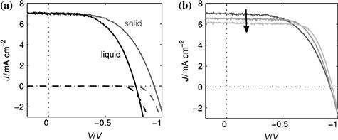
FIGURE 12 IV curves of a solid-state DSC (grey) and a liquid-electrolyte DSC (black) with D35 as sensitizer under one-sun illumination (solid line) and in the dark (dashed line).
(Taken from Figure 5.12 in reference [107].)
The efficiency of a solar cell, η, is given by
![]() (11)
(11)
where Pin is the illumination intensity and Pmax is the maximum power output of the solar cell at this light intensity. To describe the efficiency of a solar cell in terms of VOC and JSC, a quantity called the fill factor (FF) is introduced, relating Pmax to VOC and JSC:
![]() (12)
(12)
The efficiency can then be written as
![]() (13)
(13)
For the example in Figure 12, the efficiencies of the liquid DSC and sDSC were 2.9% and 3.6%, with VOC of 0.77 V and 0.93 V, JSC of 7.0 and 7.0 mA/cm2 and FF of 0.54 and 0.55, respectively. Thus, the solid-state DSC has a higher VOC than the liquid-electrolyte DSC, which is the reason for the higher efficiency of the sDSC. It should be noted that the film thickness is only 1.8 μm, so the optical density of the film is relatively low, reducing the overall efficiency. What was also observed in reference [107] and shown in Figure 12b is that in consecutive scans, the short-circuit current of the solid-state cell decreases, while the fill factor and the overall efficiency increase, demonstrating how care must be taken in measuring IV curves for DSCs, in particular for sDSCs.
With regards to illumination of the DSC cell, the cells should be masked. A mask size that is 1mm on each side bigger than the active area is recommended in reference [109]. Using thin TCO glass (ca 1 mm) and a device size of at least 5×5 mm is also recommended. This will reduce optical artefacts that can enhance or diminish the apparent power-conversion efficiency. To be qualified in the official table of world record efficiencies for photovoltaics, the solar cell area must be at least 1 cm2. For efficiency measurements of solar cells in general, we refer to [110]. For DSC specifically, we summarize the discussions above according to [111].
1. Scan rate must be slow, and the IV curve should be scanned in both directions to determine if it is slow enough.
2. The efficiency depends on premeasurement state. The temperature should be 25°C, and there should be a one-sun light bias at Pmax. Procedures that approximate this can be used. It should be noted that VOC or JSC might not give the same results as preconditioning at Pmax.
3. Light piping from outside the defined area is possible. The magnitude of this should be determined by looking at JSC with or without an aperture.
4. Quantum efficiency measurements (see below) may be nonlinear, and the results should be checked as function of light intensity. It is recommended that these measurements should be done with bias light and preferably chopped monochromatic beam.
3.3.2 External and Internal Quantum Efficiencies
The incident photon to current conversion efficiency (IPCE), sometimes also called the external quantum efficiency of the solar cell, describes how many of the incoming photons at one wavelength are converted to electrons:
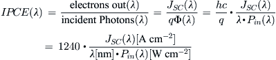 (14)
(14)
where JSC is the short-circuit current density, Φ the photon flux, Pin the light intensity at a certain wavelength λ, q the elementary charge, and h and c Planck’s constant and speed of light, respectively.
IPCEs are made typically using a xenon or halogen lamp coupled to a monochromator. The photon flux of light incident on the samples is measured with a calibrated photodiode, and measurements are typically made at 10- or 20-nm wavelength intervals between 400 nm and the absorption threshold of the dye. Since the DSC is a device with relatively slow relaxation times, it is important to make sure that the measurement duration for a given wavelength is sufficient for the current to be stabilized (normally 5–10 seconds). If it is observed that IPCE depends on light intensity, then the measurements should be made with additional bias light to ascertain that IPCE is determined at relevant light-intensity conditions. The reasons for light-intensity–dependent IPCE may be that the charge-collection efficiency (process 4 in Figure 9) increases with light intensity due to faster electron transport, or that there are mass transport limitations in the electrolyte, decreasing IPCE with light intensity.
The magnitude of the IPCE spectrum depends on how much light is absorbed by the solar cell and how much of the absorbed light is converted to electrons, which are collected:
![]() (15)
(15)
where LHE is the light-harvesting efficiency and equal to 1–10–A with A being the absorbance of the film; φinj and φreg the quantum yields for electron injection and dye regeneration, respectively; and ηCC the charge-collection efficiency.
IPCE spectra of the liquid and solid-state DSCs sensitized with D35 are shown in Figure 13 [107].
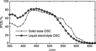
FIGURE 13 IPCE spectra of the solid-state DSC and the liquid-electrolyte DSC with D35 as sensitizer.
(Taken from Figure 5.14 in reference [107].)
The spectra are slightly different in shape, although the same TiO2 thickness and the same dye were used. The spectrum of the solid-state DSC is lower at around 380 nm and higher at the red edge of the spectrum than the spectrum of the liquid-electrolyte DSC. These differences can be explained with Equation (15): at around 380 nm, spiro-MeOTAD absorbs strongly causing a filtering effect at this wavelength in the solid-state device compared to the liquid-electrolyte DSC and therefore decreasing the IPCE. LHE at the absorption maximum of D35 was close to 1 for the devices, resulting in IPCE maxima of 80%. However, at longer wavelengths, light harvesting was incomplete. In the solid-state DSC, the reflecting back contact increased the light harvesting at these wavelengths and therefore also the IPCE.
The short-circuit current of a solar cell can be calculated by integrating over the product of the IPCE and the AM 1.5 solar spectrum:
![]() (16)
(16)
where ϕph,AM1.5 is the photon flux in AM1.5 at wavelength λ. For the DSC presented in Figure 13, the integrated JSC were determined to be 7.75 mA cm−2 for the solid-state DSC and 7.4 mA cm−2 for the liquid-electrolyte cell. These currents are slightly higher than the currents determined in the IV measurements. For the solid-state DSC, this might be due to the fact that the IPCE measurement was carried out prior to the IV measurements, so the analysis of the data must be checked according to the discussions above.
From a fundamental viewpoint, the so-called absorbed photon to current conversion efficiency (APCE) values provide further insight into the properties of the device. APCE (or internal quantum efficiency) shows how efficiently the numbers of absorbed photons are converted into current. APCE is obtained by dividing the IPCE number by the LHE (0–100%). The IUPAC name for LHE is absorptance. Thus,
![]() (17)
(17)
Quantitative in situ measurement of the light-harvesting efficiency of complete dye solar cells is complicated because of light scattering by the mesoporous oxide film and light absorption by the other cell components. For fundamental studies, it is therefore advisable to use transparent mesoporous TiO2 films. There are several descriptions of the procedures to obtain LHE in the literature—see, for example, [112–115]. As an example, we refer to the work by Barnes et al. [114] on relatively transparent TiO2 films.
To take into account reflective and absorption losses in the DSC that are not attributable to the dye–oxide system, measurement of the conducting glass, platinized counterelectrode layer, and electrolyte are made. In the example of Barnes et al., a platinized counterelectrode and a liquid I−/I3− electrolyte were used. We follow their notation and denote reflectance from the glass by R, (1 − TPt) for the absorption due to the Pt layer and (1 − TI) for the absorption in the electrolyte between the TiO2 and the Pt layer. The fraction of light transmitted by complete cells with dye (Tdye/TiO2) and without dye (TTiO2) and of film thickness d gives the absorption coefficient of the dye coated mesoporous film according to
![]() (18)
(18)
The assumptions underlying Equation (18) are that there is an exponential variation of light intensity with position in the mesoporous film and that the dye molecules do not scatter a significant fraction of light—i.e., Tdye/TiO2/TTiO2 ≈ [Tdye/TiO2/(1−Rdye/TiO2)]. Since iodine in the electrolyte, filling the oxide pores, absorbs light, one needs to take this into account by determining its absorption coefficient, αl(λ) by measuring transmission with and without iodine in the electrolyte and estimating the porosity of the films. In the work by Barnes et al. [114], relatively nonscattering TiO2 films were used and scattering effects were negligible for λ > 480 nm. To describe scattering effects, the optical measurements should be made with an integrating sphere and more sophisticated and appropriate models that include the scattering properties such as Kubelka–Munk [116].
Integration of the generation rate of excited dye states as a function of position x in the film across the thickness of the oxide film gives the LHE for illumination from the working electrode side, LHEWE, and from the counterelectrode–electrolyte side, LHECE [114]:
![]() (19)
(19)
![]() (20)
(20)
3.3.3 The DSC Toolbox
The dye-sensitized solar cell is a complex, highly interacting system. To understand the precise working mechanism of the DSC and to optimize its performance, it is important to map the energetics of the different components and interfaces and the kinetics of the different electron-transfer reactions for complete DSC devices working under actual operating conditions. The so-called toolbox of characterization techniques is used to in situ investigate the kinetics of different reactions in DSC devices. These studies are particularly fruitful, as the interactions between different components can be studied. Toolbox methods are continuously being developed by several research groups, and for two recent reviews we refer to references [21,40]. In this section, we specifically discuss the following techniques:
• photovoltage and photocurrent as a function of light intensity;
• small-modulation photocurrent and photovoltage transients to investigate electron transport and recombination;
• steady-state, quantum efficiency, measurements to determine injection efficiency, collection efficiency, and electron diffusion length;
• electron-concentration measurements;
• determination of the internal potential (quasi-Fermi level) in the mesoporous electrode; and
• photo-induced absorption spectroscopy to obtain information on recombination reactions and regeneration of the oxidized dye by the electrolyte.
A set of very powerful toolbox techniques is based on electrochemical impedance spectroscopy (EIS). The reader is referred to the works of Bisquert and co-workers on this topic, and as examples of references we propose [39,40,117]. In EIS, the potential applied to a system is perturbed by a small sine-wave modulation, and the resulting sinusoidal current response (amplitude and phase shift) is measured as a function of modulation frequency. The impedance is defined as the frequency domain ratio of the voltage to the current and is a complex number. For a resistor (R), the impedance is a real value, independent of modulation frequency, while capacitors (C) and inductors (L) yield an imaginary impedance with values that vary with frequency. The impedance spectrum of an actual system—that is, the impedance measured in a wide range of frequencies—can be described in terms of an equivalent circuit consisting of series- and parallel-connected elements R, C, L, and W, which is the Warburg element that describes diffusion processes. Using EIS, the following parameters can be obtained: series resistance, charge-transfer resistance of the counterelectrode, diffusion resistance of the electrolyte, the resistance of electron transport and recombination in the semiconductor, and the chemical capacitance of the mesoporous electrode. One of the advantages of impedance spectroscopy is that it allows simultaneous characterization of electron transport in the mesoporous oxide and of recombination of the electrons from the oxide to the hole-conducting medium. The transport and interfacial transfer of electrons in the mesoporous oxide layer can be modelled using a distributed network of resistive and capacitive elements in the form of a finite transmission line.
In the following descriptions of the toolbox techniques, we again use examples of liquid and solid-state DSCs with D35 as sensitizer.
Photovoltage and Photocurrent as a Function of Light Intensity
The short-circuit current and open-circuit voltage of a DSC can be determined as a function of light intensity. Ideally, the short-circuit current should increase linearly with light intensity. Considering Equation (15), this will be the case if the effective injection efficiency, regeneration efficiency, and collection efficiency are independent of light intensity. Plots of JSC versus light intensity for the example cells are shown in Figure 14 [107]. The gradient of the log-log plot was 1.07 for the solid-state cell and 0.99 for the liquid-electrolyte cell, showing that the currents increased almost linearly with light intensity.

FIGURE 14 Light-intensity dependence of (a) JSC and (b) VOC for the two DSCs. Dashed lines indicate fits to the data.
(Taken from Figure 5.15 in reference [107].)
If the contacts in a DSC are ohmic, the open circuit is given by the difference between the Fermi level of the semiconductor, EF, and the Fermi level of the redox electrolyte or hole conductor, EF,redox:
![]() (21)
(21)
For the liquid-electrolyte cell, the concentrations in the electrolyte do not vary significantly between the dark condition and under illumination, and therefore EF,redox can be treated as a constant (a typical value for iodide–tri-iodide is 0.31 V vs. NHE) (see Equation (3)). The voltage change at different illumination intensities therefore only depends on ln nCB. If nCB increases linearly with light intensity, then the voltage should increase by 59 mV per decade of increase in light intensity at 298 K [cf. 40]. In the example shown here (Figure 14b), the slope of a plot of VOC vs. log Pin is indeed 60 mV. Normally, however, DSCs are nonideal to some extent, and generally the photovoltage varies by more than 59 mV per decade of intensity (values as high as 110 mV/decade are not uncommon). The origin of this nonideality is not understood, but it has important consequences for the interpretation of many of the techniques discussed in this chapter. An empirical nonideality factor, m (>1), is often used to account for nonideality so that the intensity dependence of the photovoltage is given by
![]() (22)
(22)
In the case of solid-state DSCs, the relative concentrations of oxidised spiro-MeOTAD and ground-state spiro-MeOTAD are not as well known as the ratio of I3− and I− in the liquid electrolyte. Therefore, EF,redox in the dark is not as well known as for the liquid-electrolyte cell. If Cox is very small, then the concentration of holes injected under illumination might significantly influence the EF,redox of spiro-MeOTAD and therefore VOC. The slope of a plot of VOC vs. log Pin for the solid-state cell (Figure 14b) was 80 mV. This higher value could be due to an effect of the change of concentration of oxidised spiro-MeOTAD under illumination, but other nonideality effects such as recombination of electrons to the hole conductor via surface states also may be important.
Small-Modulation Photocurrent and Photovoltage Transients to Investigate Electron Transport and Recombination
Information about the transport and lifetimes of charge carriers in the DSC can be obtained by monitoring the current and voltage transients following a small modulation of the light intensity. Figure 15a shows normalised photocurrent transients of the solid-state DSC and the liquid-electrolyte DSC measured under short-circuit conditions at the same bias light intensity [107]. Due to the small amplitude of the modulation, the transients can be reasonably well fitted by a single exponential decay:
![]() (23)
(23)
where τresp is the characteristic time constant of the decay. A plot of τresp measured at different bias light intensities can be seen in Figure 15b. The photocurrent response times of the solid-state DSC are significantly faster than the corresponding time constants for the liquid-electrolyte DSC at the same short-circuit current.
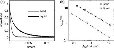
FIGURE 15 (a) Normalised current decays of the two DSCs at the same bias light intensity (560 W m−2) following a small downward modulation of the light intensity. (b) Photocurrent response times obtained from fits at different light intensities as a function of JSC. Dashed lines indicate a log-log fit to the data.
(Taken from Figure 5.17 in reference [107].)
The time constant of the current decay depends on how fast the system adjusts to the decreased injection of charges into the TiO2. It therefore depends on the recombination rate and on the rate at which charge carriers can be transported out of the cell. Considering that both holes and electrons have to be transported out of the cell independently, it will depend on the limiting one of these two types of charge transport. For a liquid-electrolyte DSC, this is the electron transport in the TiO2. The transport of I3− to the counterelectrode can usually be ignored because an excess of I3− is available in the electrolyte. τresp can then be related to the transport time of electrons in the TiO2 (τtr) and to the electron lifetime (τe) by
![]() (24)
(24)
For optimised liquid-electrolyte cells under short-circuit conditions, τe is much larger than τtr, and the photocurrent response time becomes a direct measure of the electron-transport time in the TiO2. The chemical diffusion coefficient, De, can be calculated from the electron-transport time using Equation (25):
![]() (25)
(25)
where d is the thickness of the mesoporous oxide film and C is a constant with a value of about 2.5, which depends slightly on absorption coefficient of the film and direction of illumination [118–119].
For the sDSC, it seems possible that the charge transport could be limited by the transport of holes to the back contact if the concentrations of oxidised spiro-MeOTAD is very low [see reference 107 and references therein]. However, in such a case an increase in τresp would be expected compared to a comparable liquid-electrolyte DSC. The reason for the shorter transport time for sDSC is unclear.
One method to measure τe is to measure the photovoltage decay, the VOC decay method [21,120]. Here the open-circuit potential of a DSC is monitored as function of time when the light is switched off. The electron lifetime is calculated from the slope of the VOC transient:
![]() (26)
(26)
An advantage of this method is that the lifetime can be determined in a wide potential range with one single measurement. It can also be performed without using light by application of a negative potential before open-circuit decay [121].
The charge-collection efficiency, ηCC, can be estimated from electron transport and lifetime measurements as follows [122]:
![]() (27)
(27)
For a correct calculation of the charge-collection efficiency, the transport time and lifetime must be measured at the same quasi-Fermi level (electron concentration) in the mesoporous electrode. If τresp (measured at short circuit) and τe (measured at open circuit) are used to calculate ηCC, then the resulting value will underestimate the true ηCC value under short-circuit conditions. To determine the latter, τe must be determined under conditions where the quasi-Fermi level in the mesoporous oxide is equal to that under short-circuit conditions. This can be achieved by (1) measuring the quasi-Fermi level under short-circuit conditions (see the following discussion) and determining τe from the relation between τe and VOC or (2) measuring the extracted charge under short-circuit conditions and determining τe from the relation between τe and the extracted charge (see below). Electrochemical impedance spectroscopy [123] and photovoltage rise or decay measurements (see the following discussion) can be used to determine τtr and τe simultaneously at the same quasi-Fermi level. The charge-collection efficiency can also be determined from IPCE using Equation 15.
The electron diffusion length, L, in the DSC is closely related to the charge-collection efficiency. L is a wavelength independent parameter, whereas ηCC depends on wavelength. Södergren et al. derived expressions for the IPCE of mesoporous DSCs as a function of the diffusion length, absorption coefficient, and film thickness, assuming quantitative electron injection [44], see the following discussion. In recent works by Halme et al. [113] and Barnes et al. [114] these relations were used to determine the electron diffusion length in DSCs under various conditions. Dynamic, small amplitude methods (impedance spectroscopy, electron-transport, and lifetime measurements) can also be used to determine the electron diffusion length [124,125].
![]() (28)
(28)
where De is the effective electron diffusion coefficient. Interestingly, the values of L determined in this way were at least a factor 2 larger than those obtained from IPCE measurements [126]. Bisquert and Mora-Sero [127] demonstrated in a simulation study that this can be attributed to the fact that recombination kinetics in DSCs are nonlinearly dependent on the electron concentration in the conduction band, whereas linearity is assumed in the IPCE method. Recently, a careful comparison has been made between values of the diffusion length obtained by impedance spectroscopy and by front- or rear-side IPCE measurements using bias light, showing that the methods agree if measurements are made close to open circuit to ensure that the electron concentration across the film is almost constant [128].
An alternative technique devised to measure electron-transport time in DSCs is a photovoltage rise method [129]. Here the cell is kept under open-circuit conditions, and the characteristic time constant for photovoltage rise is measured after application of a short light pulse superimposed on a constant bias illumination. The electron-transport time is calculated from the rise time using the capacity values of the mesoporous oxide and the substrate–electrolyte interface, which have to be measured independently. The electron lifetime is determined in the same experiment from the voltage decay. The advantage of this method is that it can be performed under conditions where the resistance-capacitance (RC) time constant of the DSC, arising from the series resistance of the mesoporous oxide and conducting substrate and the large capacity of the mesoporous film, does not limit the transport measurement.
Steady-State (Quantum Efficiency) Measurements to Determine Injection Efficiency, Collection Efficency, and Electron Diffusion Length
Under steady-state conditions, the rate of trapping and detrapping must be equal so the presence of trap states will not have any influence on, for example, the electron diffusion length or the charge-collection efficiency. Thus, steady-state measurements avoid some of the complications involved in finding the electron diffusion coefficient, L, by perturbation frequency domain or transient methods. A standard steady-state method is measurement of the IPCE spectrum. Comparison of spectral IPCE measurements taken for opposite illumination directions is not only a good diagnostic test for detecting low ηCC but also provides basis for quantitative estimation of L by the diffusion model. The derivation can be found in references [40,44,113,114]. The model assumes that the electron transport occurs via diffusion, the recombination reactions are first order in the electron concentration, De and τ are independent of x and n(x), and that under short-circuit conditions, extraction of electrons at the substrate contact is fast enough to keep the excess electron concentration at the contact close to the dark equilibrium value.
The ratio between the IPCE, or APCE, spectra, which depends only on α(λ), d and L since ηinj(λ) can be assumed independent of the direction of illumination, is expressed as
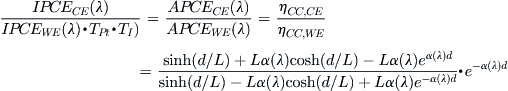 (29)
(29)
Two special cases can be considered with respect to uniform or highly nonuniform electron generation. For uniform generation, obtained in the limit of weak light absorption, ηCC becomes
![]() (30)
(30)
and independent of the illumination direction. In the opposite case 1/α << d, corresponding to high LHE, ηCC approaches 100% for the WE illumination, whereas for the CE illumination it becomes
![]() (31)
(31)
The main predictions from the preceding equations can be summarized as [113]:
1. For constant L and α, ηCC decreases with d for the both directions of illumination.
2. For L much larger than d, ηCC approaches 100%, irrespective of α and the direction of illumination.
3. For uniform electron generation obtained in the limit of weak light absorption, ηCC becomes equal at the both illumination directions, irrespective of d and L.
4. For constant d and L, ηCC increases with α at the WE illumination; at the CE illumination, the trend is opposite.
Using the experimental data for APCECE/APCEWE, d, and α, L can be estimated directly from Equation (29) for each λ and d. With the estimated L, ηCC can be calculated from Equations (30) and (31), and ηinj subsequently as
![]() (32)
(32)
It should be noted that a fit to the IPCE ratio, Equation (29), is independent of calibration errors in the IPCE measurement (the ratio can be normalized to unity at long wavelengths if the losses due to Pt and iodine are uncertain) [114].
Electron Concentration Measurements
The total concentration of electrons in the mesoporous oxide film under solar cell operating conditions can be determined using different methods [21,40]. In charge-extraction methods, the light is switched off and all remaining charge in the film is extracted as a current during a certain period and integrated to obtain the charge. Under short-circuit conditions, this simply corresponds to the integration of the photocurrent transient recorded after the light is switched off [130,131]. Starting from open-circuit conditions, the cell connection has to switch from open to short-circuit simultaneously with switching off of the light. When the VOC is allowed to decay in the dark for different periods before charge extraction, a complete charge-potential curve can be obtained by repeated experiments [132]. When charge-extraction measurements are used, it should be realized that not all electrons will be extracted due to recombination losses and limitations in extraction time (electron transport becomes very slow at low electron concentrations).
In an alternative method, the capacity of the mesoporous film is measured rather than the charge [133]. At a certain open-circuit potential obtained by bias illumination, a light pulse is added and the resulting voltage rise is measured. The photocurrent transient resulting from the light pulse is measured separately under short-circuit conditions and used to calculate the injected charge induced by the light pulse. The capacity is calculated from the ratio of injected charge and voltage change. Integration of capacity with respect to the range of open-circuit potentials gives the charge-potential relation.
Finally, near-infrared transmission measurements can be done to determine the total electron concentration in mesoporous dye-sensitized solar cells [134]. An optical cross section of 5.4×1018 cm2 was determined at 940 nm for electrons in mesoporous TiO2, corresponding to a decadic extinction coefficient of 1400 M−1 cm−1, in good agreement with spectroelectrochemical studies on mesoporous TiO2 (1200 M−1 cm−1 at 700 nm) [135].
Approximate electron concentrations in the mesoporous TiO2 film of a DSC under operating conditions (one sun) are on the order of 1018–1019 cm−3 [134,136] corresponding to about 4–40 electrons per TiO2 particle, assuming spherical 20-nm sized particles.
Determination of the Internal Potential (Quasi-Fermi Level) in the Mesoporous Electrode
Two methods have been developed to determine the quasi-Fermi level in mesoporous oxide electrodes. The first method is a switching method and can be performed on standard DSCs [136,137]. The DSC is illuminated under short-circuit conditions (or kept at a certain applied potential), when simultaneously the light is switched off and the cell is switched to open circuit while the potential is measured. The potential will rise to reach a value that is similar to the quasi-Fermi level of the electrons in the mesoporous film, as it was present in the illuminated film. Considering that there was a gradient in the Fermi level, the resulting value will be an average value. Model calculations suggest that even under short-circuit conditions, the Fermi level under illumination conditions is relatively flat in the whole mesoporous film, except for about 1 μm directly adjacent to the conducting substrate, so that the measured value gives a good indication of the Fermi level in most of the film. Additionally, the rise of the potential gives information on the electron transport in the mesoporous film, and the following decay of the potential information on the electron lifetime.
In the second method, the deposition of an additional titanium electrode on top of a mesoporous TiO2 film was made [138,139]. The surface of the metal is passivated by thermal oxidation and does not lead to an additional recombination pathway for electrons in the TiO2. The potential of the additional electrode can be measured under operating conditions and directly gives the quasi-Fermi level at the outside of the mesoporous TiO2 film. Both methods give similar results and show that in standard DSCs, illuminated at one sun, the quasi-Fermi level under short circuit in the mesoporous TiO2 is located about 0.5–0.6 V negative of the redox potential of the electrolyte.
Photo-Induced Absorption Spectroscopy to Obtain Information on Recombination Reactions and Regeneration of the Oxidized Dye by the Electrolyte
Transient absorption spectroscopy (TAS) is a common tool for the study of the kinetics of DSCs [96,140–144]. Usually, the change in absorption of a visible probe light by a dyed TiO2 film is measured as a function of time following excitation of the dye by a short laser pulse (the pump). This technique is also referred to as laser flash photolysis, and kinetics can be measured on different timescales, depending on the equipment and the laser pulse length. When using a femtosecond laser to generate both the pump and the probe pulse, kinetics in the femto- and picosecond time scales can be resolved (electron injection and regeneration in solid-state DSCs). When lasers with nanosecond long pulses are used, the probe light is often supplied by a separate lamp, and kinetics on the nano- and microsecond timescales can be resolved (regeneration in liquid-electrolyte DSCs and recombination). To create a detectable concentration of transient species, TAS often requires the use of high light intensities in the pump.
As a toolbox technique, we have developed photo-induced absorption (PIA) spectroscopy [145,146]. In PIA, the difference in absorption between a pump light being on and off is measured as a function of modulation frequency and probe wavelength. As the on time of the pump is relatively long in these experiments (55 ms at a 9 Hz modulation), light intensities similar to the light intensities under operating conditions of the solar cell can be used. The kinetics of slower processes in the DSC (t > 10−5 s) can be followed using PIA—e.g., recombination of electrons in the oxide with oxidized dyes or electrolyte species. It is very useful in qualitative studies, for instance, to check whether a dye is injecting electrons into the oxide after photoexcitation and whether a dye is regenerated when in contact with a redox electrolyte. PIA can also be measured over a large wavelength range and the measurements are relatively fast (acquisition of a spectrum often takes only 10 minutes) and very easy to set up and use.
A schematic diagram of the PIA setup in our laboratory is shown in Figure 16. A white probe light, provided by a 20-W tungsten-halogen lamp, is focused onto the sample by a series of optics. Superimposed at the sample is the pump light used for excitation. Typical excitation intensities at the sample are between 8 and 25 mWcm−2, and typical probe intensities are between 10% of 1 sun and 40% of 1 sun. The pump light can be chosen between a blue LED (Luxeon Star, 1W, Royal Blue, 460 nm), a green LED-pumped laser at 530 nm, or a red-diode laser at 640 nm. The pump light is square-wave modulated (on–off) with a function generator.
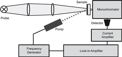
After transmission through the sample, the probe light is focused onto a monochromator and detected by a UV-enhanced silicon photodiode, allowing for measurements between 400 and 1100 nm. The detector is connected to a current amplifier and a lock-in amplifier. The lock-in amplifier is locked to the modulation frequency, such that ΔT/T in phase with the modulation frequency (the “real” part of ΔT/T, Re(ΔT/T)) and ΔT/T out of phase with the modulation frequency (the “imaginary” part of ΔT/T, Im(ΔT/T)) are measured. In this way, only signals occurring at the modulation frequency are detected, which greatly enhances the signal to noise ratio. The setup allows the measurement of ΔA at different wavelengths, resulting in the measurement of a photo-induced absorption spectrum at a given frequency and the measurement of ΔA at different frequencies (frequency-resolved PIA at a given λ). Additionally, ΔA can also be measured as a function of time—i.e., individual time traces following the rise and decay of ΔA can be obtained.
For the theory of PIA measurements we refer to references [107,145,146]. As the concentrations of transient species (and therefore their absorbances) depend on recombination rates, only processes with a relatively long lifetime (milliseconds to seconds) can be resolved with PIA. A sample of, for example, dyed TiO2 therefore only shows a signal of oxidised dye molecules if recombination times are sufficiently long. This is often the case, and PIA can show if effective injection is happening. When a redox electrolyte or hole conductor are added to such a sample and the regeneration of oxidised dye is fast and efficient, the “lifetime” of the oxidised dye becomes very short. Consequently, the concentration of oxidised dye is decreased by many orders of magnitude, and the PIA signal of oxidised dye will be negligible. Instead, a signal due to holes and electrons will be observed. PIA can therefore show if the regeneration of oxidised dye molecules is efficient. An example of such a study is presented in Figure 17. In this figure we used a perylene organic dye as sensitizer, the ID28 dye [107] and spiro-MeoTAD as hole conductor. Without the hole conductor the photoexcited dye injects electron in the TiO2 and the spectrum of the oxidized dye is observed (solid line). With the hole conductor (dashed line) there are no remaining features of the oxidized dye, indicating an efficient regeneration of the oxidized dye.

FIGURE 17 Example of a PIA study using (a) the ID28 perylene dye on TiO2 and (b) with the addition of the spiro-MeoTad hole conductor [107].
To use PIA for quantification of the injection and regeneration efficiencies, however, is difficult. First, one needs to choose a wavelength at which the Stark effect (this effect is described below) of the dye is not observed. Then one needs to determine the rate constant of recombination and the order of recombination by measuring and fitting frequency-resolved PIA at different light intensities. Finally, any values of injection and regeneration efficiencies will include any recombination that occurs on faster time scales than the PIA measurement.
3.3.4 The Stark Effect in DSC
Electric fields can induce a change in the transition energies of molecules (ΔE) [147–149]. This is called the Stark effect, electroabsorption, or electrochromism. Recently, it has been shown that a potential drop across dye molecules in DSC systems upon electron injection into TiO2 leads to a Stark shift of the absorption spectra of dyes [5,6,77,150]. In very general terms, the change in transition energy due to an external electric field (![]() ) is given by
) is given by
![]() (33)
(33)
where Δμ is the change in dipole moment and Δα is the change in polarisability due to the transition. This equation is valid for electronic transitions as well as for other transitions. One distinguishes the first-order Stark effect, which is linear in the electric field, and the second-order Stark effect, which is quadratic in the electric field. Considering dye-sensitized solar cells, we are interested in how the Stark effect affects electronic transitions of dye molecules that are adsorbed to titanium dioxide surfaces. The effect will be induced by electrons injected into the titanium dioxide. We can define a main direction of the electric field, which is normal to the titanium dioxide surface, assuming for simplification that the positive countercharges are uniformly distributed at a certain distance away from the TiO2 particle (Figure 18a). On average, dye molecules adsorbed to the surface should therefore experience an almost uniform electric field in one direction (Figure 18b) and we can rewrite Equation (33) in a one-dimensional form (chosen to be along the z-axis here):
![]() (34)
(34)
However, it is the change in absorbance (ΔA) due to an electric field rather than the change of transition energy, which is of practical interest. An expression for ΔA can be derived from a Taylor expansion of A around E at Fz = 0:
![]() (35)
(35)
Substituting ΔE from Equation 34 into this equation, one can obtain an expression for the terms of ΔA linear and quadratic with the electric field:
![]() (35)
(35)
Organic dyes used in DSCs are usually designed to have a large change in dipole moment upon excitation and should therefore show a first-order Stark effect, given by the linear term of Equation (35). A representation of this first-order Stark effect is shown in Figure 18c. For organic donor-acceptor (push-pull) dyes designed for n-type DSCs, Δμz usually points away from the TiO2 surface (electron density is moved towards the TiO2 surface upon excitation). The transition energies are therefore expected to increase upon electron injection into the TiO2, and the absorption spectrum is expected to shift to shorter wavelengths. The Stark effect has been observed in different types of measurements of DSC systems, such as in the following [107]:
• photo-induced absorption and transient absorption measurements where the Stark effect of ground-state dye molecules was observed both in absence and presence of a redox mediator after photo-induced electron injection [5,6,77];
• electroabsorption measurements where an external electric field was applied to a monolayer of dye molecules adsorbed to a flat TiO2 substrate [5,77]; and
• spectroelectrochemistry, where charges were injected into a dye-coated mesoporous TiO2 film surrounded by a supporting electrolyte by applying a negative potential to the film [107 and refs. therein].
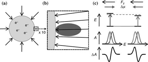
FIGURE 18 (a) Electric field direction outside a titanium dioxide particle with a 20-nm diameter into which electrons have been injected. A dye molecule with a length of 2 nm and a width of 1 nm is included. (b) Enlargement of the dye molecule on the surface. The electric field lines around the dye molecule are almost parallel. (c) Representation of the first-order Stark shift when Δμz is antiparallel to Fz and Δμz is parallel to Fz.
(Taken from Figure 4.2 in reference [107].)
3.4 Development of Material Components and Devices
Since the initial work in the beginning of the 1990s, a wealth of DSC components and configurations have been developed. Perhaps a key concept for the future success of DSC is diversity. At present, several thousands of dyes have been investigated as well as numerous types of mesoporous films with different morphologies and compositions. The last year has seen some very interesting breakthroughs in the use of alternative redox systems, and this field is now opened up after almost 20 years of I−/I3− dominance. With such a diversity to explore, the DSC technology can be expected to progress rapidly, be it through design of new materials and combinations based on fundamental insights or by evolution—i.e., trial and error—or better, with the use of combinatorial approaches.
In the following sections, we briefly overview the development of the material components and devices in DSC and in general refer to the many recent reviews on these topics.
3.4.1 Mesoporous Oxide Working Electrodes
The key to the breakthrough for DSCs in 1991 was the use of a mesoporous TiO2 electrode with a high internal surface area to support the monolayer of a sensitizer. Typically, the increase of surface area by using mesoporous electrodes is about a factor 1000 in DSCs. TiO2 still gives the highest efficiencies, but many other metal oxide systems have been tested, such as ZnO, SnO2, and Nb2O5. Besides these simple oxides, ternary oxides, such as SrTiO3 and Zn2SnO4, have been investigated, as well as core-shell structures, such as ZnO-coated SnO2. For recent reviews on the development of nanostructured metal oxide electrodes for DSC, the reader is referred to references [1,21,151–154]. During the last few years, large efforts have been paid to optimize the morphology of the nanostructured electrode, and a large range of nanostructures has been tested from random assemblies of nanoparticles to organized arrays of nanotubes and single-crystalline nanorods. These studies are motivated by the expectation of an improved and directed charge transport along the rods and tubes and by an improved pore filling of hole conductor materials for solid-state DSC. General reviews for preparation techniques and structures are, for example, Chen et al. for TiO2 [155] and Ozgur et al. for ZnO [156].
TiO2 is a stable, nontoxic oxide that has a high refractive index (n = 2.4–2.5) and is widely used as a white pigment in paint, toothpaste, sunscreen, self-cleaning materials, and food (E171). Several crystal forms of TiO2 occur naturally: rutile, anatase, and brookite. Rutile is the thermodynamically most stable form. Anatase is, however, the preferred structure in DSCs, because it has a larger band gap (3.2 vs. 3.0 eV for rutile) and a higher conduction band edge energy, Ec. This leads to a higher Fermi level and VOC in DSCs for the same conduction band electron concentration.
For state-of-the-art DSCs, the employed architecture of the mesoporous TiO2 electrode is as follows [21 and refs. therein]:
1. A TiO2 blocking layer (thickness ~50 nm), coating the FTO plate to prevent contact between the redox mediator in the electrolyte and the FTO, prepared by chemical bath deposition, spray pyrolysis, or sputtering.
2. A light absorption layer consisting of a ~10-μm thick film of mesoporous TiO2 with ~20-nm particle size that provides a large surface area for sensitizer adsorption and good electron transport to the substrate.
3. A light scattering layer on the top of the mesoporous film, consisting of a ~3-μm porous layer containing ~400-nm-sized TiO2 particles. Voids of similar size in a mesoporous film can also give effective light scattering.
4. An ultrathin overcoating of TiO2 on the whole structure, deposited by means of chemical bath deposition (using aqueous TiCl4), followed by heat treatment.
3.4.2 Dyes
As one of the crucial parts in DSCs, the photosensitizer should fulfill some essential characteristics:
1. The absorption spectrum of the photosensitizer should cover the whole visible region and even the part of the near-infrared (NIR).
2. The photosensitizer should have anchoring groups (–COOH, –H2PO3, –SO3H, etc.) to strongly bind the dye onto the semiconductor surface.
3. The excited state level of the photosensitizer should be higher in energy than the conduction band edge of n-type DSCs, so that an efficient electron-transfer process between the excited dye and conduction band of the semiconductor can take place. In contrast, for p-type DSCs, the HOMO level of the photosensitizer should be at more positive potential than the valence band level of the p-type semiconductor.
4. For dye regeneration, the oxidized state level of the photosensitizer must be more positive than the redox potential of electrolyte.
5. Unfavourable dye aggregation on the semiconductor surface should be avoided through optimization of the molecular structure of the dye or by addition of coadsorbers that prevent aggregation. Dye aggregates can, however, be controlled (H- and J-aggregates), leading to an improved performance compared with a monomer dye layer as, for example, described in reference [157].
6. The photosensitizer should be photostable, and electrochemical and thermal stability are also required.
Based on these requirements, many different photosensitizers including metal complexes, porphyrins, phthalocyanines, and metal-free organic dyes have been designed and applied to DSCs in the past decades. Ru-complexes have since the early days given the best results. Osmium and iron complexes and other classes of organometallic compounds such as phthalocyanines and porphyrins have also been developed. These dyes have recently been reviewed [21,158]. Metal-free organic dyes are catching up, showing efficiencies close to 10% with the use of indoline dyes. Moreover, chemically robust organic dyes showing promising stability results have recently been developed by several groups. Organic dyes for DSCs have been reviewed in references [21,159].
During the last 2 to 3 years, the advent of heteroleptic ruthenium complexes furnished with an antenna function has taken the performance of the DSC to a new level [21 and refs. therein]. An example of these dyes is C101 (see Figure 6). Compared with the classical N3, N719, and black dye, its extinction coefficients is higher and the spectral response is shifted to the red. Efficiencies above 12% have been reported [20]. The C101 sensitizer furthermore maintains outstanding stability at efficiency levels more than 9% under light soaking at 60°C for more than 1000 h [60]. This is achieved by the molecular engineering of the sensitizer but also very importantly by the use of robust and nonvolatile electrolytes, such as ionic liquids and adequate sealing materials.
A common line of development for organic dyes in DSCs is to synthesise so-called D-π-A dyes that consist of an electron donor (D), a conjugated linker (π), and an electron acceptor (A). The idea behind this concept is that in such molecules, most of the electron density of the HOMO will be located on the donor, while most of the density of the lowest unoccupied molecular orbital (LUMO) will be located on the acceptor. The dyes therefore show intramolecular charge transfer from the donor to the acceptor upon excitation. For typical n-type dyes used in standard DSCs, the anchoring group is located close to or is even part of the acceptor. This ensures that the excited state of the dye is located closer to the TiO2 surface than the hole remaining on the dye after electron injection. This should help to supress recombination between electrons and oxidised dye molecules and make the hole easily accessible for the redox mediator, which is beneficial for regeneration. A variation of this theme is employed in p-type DSCs, which use a p-type semiconductor (NiO) as a photocathode [160–162]. In these DSCs, a hole is injected into the semiconductor and therefore the anchoring group will now be on the donor of the sensitizer, facilitating hole injection. A p-type DSC can be combined with the conventional n-type DSC into a tandem DSC device. See references [1,21] for recent reviews on these systems.
The donor, acceptor, and linker of the molecule can then be independently varied to tune the properties of the molecules [21]. Typically used donors are triphenylamine, indoline, or coumarin units. Examples of acceptors, which include anchoring groups, are cyanoacrylic acid and rhodanine-3-acetic acid. Another modification often made to organic dyes is to introduce alkyl chains to the linker or donor part of the molecule. These can prevent the formation of dye aggregates or inhibit electron and hole recombination by protecting the TiO2 surface. An example of such a dye based on a triphenylamine donor is D35 [163,164] (Figure 11), which has been successfully employed in both liquid-electrolyte and solid-state DSCs.
3.4.3 Electrolytes
There are many demands on the electrolyte or hole conducting material. They should be chemically stable; provide good charge-transport properties; not dissolve the dye from the oxide surface or the oxide, counterelectrode, and substrates; and be compatible with a suitable sealing material to avoid losses by evaporation or leakage. Several types of electrolyte and hole conductor materials have been developed over the years.
The standard redox electrolyte for DSC ever since the very start in 1991 now comprises the iodide–tri-iodide (I−/I3−) redox couple in an organic solvent. It has good solubility and a suitable redox potential, and it provides rapid dye regeneration. A serious disadvantage of this redox mediator is that a significant part of the potential is lost in the regeneration of the oxidized dye due to intermediate reactions [73]. To develop dye-sensitized solar cells with efficiencies significantly larger than 12%, our strategy was to use one-electron redox couples or hole conductors instead of I−/I3−. Unfortunately, the use of one-electron mediators in DSC nearly always leads to strongly increased recombination between electrons in TiO2 and the oxidized part of the redox couple, which seriously limits the solar cell efficiency. Recently, however, we obtained a breakthrough with cobalt polypyridine-based mediators in combination with the organic dye, D35. Careful matching of the steric bulk of the mediator and the dye molecules minimizes the recombination between electrons in TiO2 and Co(III) species in the electrolyte and avoids mass transport limitations of the redox mediator. The organic sensitizer D35, equipped with bulky alkoxy groups, efficiently suppresses recombination, allowing the use of cobalt redox mediators with relatively small steric bulk. The best efficiency obtained for a DSC sensitized with D35 and employing a [Co(bpy)3]3+/2+-based electrolyte was 6.7% at full sunlight (1000 W m−2 AM1.5G illumination) [7], which is more than a doubling of previously published record efficiencies using similar cobalt-based mediators. We could thus show that the dye layer itself could efficiently suppress the recombination of electrons in the TiO2 with oxidized species in the electrolyte opening up the possibilities to use alternative redox couples. With the recent world record of 12.3% using Co-complexes by Grätzel and co-workers [8,165] the main direction of the research field is now to explore this path. Interesting results are also currently presented using other redox systems such as organic redox couples [166,167], ferrocenes [168], and Cu-complexes [169].
Alternative redox systems have been developed over the years such as Br−/Br3− [170], SCN−/(SCN)3− [171], SeCN−/(SeCN)3− [172], and organic redox systems such as TEMPO [173]. For practical applications, it is preferable to use a low-volatility electrolyte system simplifying production processes, encapsulation methods, and materials. Ionic liquids and gel electrolytes are also normally based on I−/I3− [174]. Solid-state DSC [175] have developed quickly recently using the spiro-MeOTAD hole conductor with efficiencies above 5% and recently above 7% [8], but interesting results are also obtained with conducting polymers such as P3HT [176] and inorganic p-type semiconductors such as CuSCN [177] and CuI [178]. The electrolyte–hole conductor systems have recently been reviewed in reference [21].
3.4.4 Counterelectrodes
Counterelectrodes for DSCs with iodide–triiodide electrolytes can be rather easily prepared by deposition of a thin catalytic layer of platinum onto a conducting glass substrate. Without platinum, conducting tin oxide (SnO2:F) glass is a very poor counterelectrode and has a very high charge-transfer resistance, more than 106 Ω cm2, in a standard iodide–tri-iodide electrolyte [179]. Pt can be deposited using a range of methods such as electrodeposition, spray pyrolysis, sputtering, and vapour deposition. Best performance and long-term stability has been achieved with nanoscale Pt clusters prepared by thermal decomposition of platinum chloride compounds [180]. In this case, very low Pt loadings (5 μg cm−2) are needed so that the counterelectrode remains transparent. Charge-transfer resistances of less than 1 Ω cm2 can be achieved.
Alternative materials are, for example, carbon, which is suited as a catalyst for the reduction of tri-iodide [181] and provides good conductivity [182]. Films prepared on TCO substrates from carbon powders and carbon nanotubes showed good catalytic activity for I3− reduction as well as good conductivity [183–186]. Conducting polymers have been successfully developed, PEDOT doped with toluenesulfonate anions in particular [187–189]. Recently, metal (Co, W, Mo) sulfides have been identified as suitable catalysts for the I−/I3− redox couple [190–192].
3.4.5 Development of Modules
The manufacturing, reliability, performance, and stability of a DSC module are more complex compared with the test cell situation due to the larger size. Moreover, interconnected cells in a DSC module may interact through, for example, mismatched performance of the cells or unwanted mass transport of electrolyte between adjacent cells. The dominating DSC module designs can be divided into five categories [21] and as schematically shown in Figure 19. In the figure caption, the term sandwich is used to define a device structure carrying the working and the counterelectrodes on two substrates. The term monolithic is used to define a device structure carrying the working and counterelectrode on one and the same substrate. Figure 20 is an example of a monolithic module prepared at Swerea IVF AB, Sweden. In the present table of record solar cell efficiencies a DSC module efficiency of 9.2% is listed, achieved by Sony, Japan [4].

FIGURE 19 Schematic cross sections of examples of constructions of the five categories of DSC modules: (a) sandwich Z-interconnection; (b) sandwich W-interconnection; (c) sandwich current collection; (d) monolithic serial connection; (e) monolithic current collection. Each module consists of four working and counterelectrodes. The proportions of the module layers and substrates are not drawn to scale but have been adjusted to illustrate the device constructions.
(Taken from Figure 21 in reference [21].)
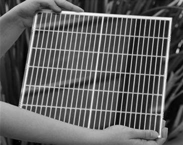
FIGURE 20 A 900-cm2 demonstrator consisting of 12 parallel-connected modules that are connected in series. The cell width is 8 mm, and the amount of active area is 75%.
As described above, there are many different DSC module designs, substrates, and manufacturing combinations. According to us, it is still too early to identify a winning combination. Clearly, the monolithic concept offers a cost advantage because only one substrate is used. Likewise, the use of flexible substrates, polymers or metal foils, allow for rapid manufacturing using, for example, roll-to-toll processes. However, the highest module efficiencies have been obtained on glass-based sandwich modules. The performance of the described DSC module designs may be increased by improved device components—for example, TCO glass and dye, or closer packaging of cells, or a less inactive area. The latter can, for the designs utilizing current collectors or interconnects, be obtained by using an inert combination of electrical conductor and electrolyte. Various companies have in the last years reported such DSC systems. Unfortunately, the DSC technology is not so trivial that the highest module efficiency, the fastest production methods, or the lowest materials cost necessarily provides the best module solution. The big challenge is to produce reliable devices that are long-term stable to fulfill the requirements of the designed application. It may thus be that a winning combination springs from the most functional encapsulation method.
4 Future Outlook
With time, the chemical complexity of DSCs has become clear, and the main challenge for future research is to understand and master this complexity, in particular at the oxide–dye–electrolyte interface. Thus, for future research, it will be important to carefully select several reference systems that emphasize different key aspects of the device and characterize these systems in depth with all the different techniques we have at hand. From comparisons and modelling, we may then find a better generality of our fundamental understanding.
A challenging but realizable goal for the present DSC technology is to achieve efficiencies above 15%. The new one-electron–based redox couples may significantly lower the voltage drop between the redox system and the oxidized dye, thus pointing out the direction to reach above 15%. This will require electron-transfer studies to clarify how much driving force is needed in the regeneration step and how this can be optimized by tuning of the redox potential by modification of the redox complexes and the oxidation potential of the dye. Moreover, the blocking of the recombination reaction of electrons in the oxide with electrolyte species is an important task for further design of dye molecules and surface passivation methods.
Regarding stability of DSC cells and modules, the conditions for accelerated testing have not yet been standardized. Until now, 1000-h light-soaking and 1000-h high-temperature storage tests have mainly been performed to compare materials and to show feasibility of the technology. As the technology advances, the outcome of accelerated testing will also be used to start calculating acceleration factors and estimating product life. Since this is not straightforward, intensified research and development is urgently required to define the procedures for relevant accelerated testing of dye-sensitized solar devices. Especially important is collecting outdoor test results from different locations and application-relevant conditions. The outcome needs to be related to results from accelerated testing to define the key tests for accelerated testing of DSC modules.
For the DSC technology, it is advantageous to compare energy cost rather than cost per peak watt. DSCs perform relatively better compared with other solar cell technologies under diffuse light conditions and at higher temperatures. An overall goal for future research will thus be to collect data and develop models to make fair judgments of the DSC technology with regards to energy costs.
With the ever-increasing industrial development of the DSC technology, we anticipate some exciting years to come with possible introduction of niche applications such as consumer electronics and successful development of manufacturing processes.
References
1. Gibson EL, Hagfeldt A. Solar energy materials. In: Bruce DW, O’Hare D, Walton RI, eds. Energy Materials. John Wiley & Sons, Ltd. 2011; 978-0-470-99752-9, Chapter 3.
2. Green MA, Emery K, Hishikawa Y, Warta W. Prog Photovoltaics. 2008;16:435.
3. Chib Y, Islam A, Kakutani K, Komiya R, Koide N, Han L. High efficiency dye- sensitized solar cells Technical Digest. Shanghai: 15th International Photovoltaic Science and Engineering Conference; October 2005; 665.
4. (i)Green MA, Emery K, Hishikawa Y, Warta W. Prog Photovolt: Res Appl. 2010;18:346.
4. (ii)Morooka M, Noda K. Tokyo: 88th Spring Meeting of the Chemical Society of Japan; 26 March 2008;.
5. Cappel UB, Feldt SM, Schoeneboom J, Hagfeldt A, Boschloo G. J Am Chem Soc. 2010;132:9096.
6. Ardo S, Sun Y, Staniszewski A, Castellano FN, Meyer GJ. J Am Chem Soc. 2010;132:6696.
7. Feldt SM, Gibson EA, Gabrielsson E, Sun L, Boschloo G, Hagfeldt A. J Am Chem Soc. 2010;132:16714.
8. Grätzel M. Valencia, Spain: Keynote lecture, 3rd Hybrid and Organic Photovoltaics Conference; May 15–18, 2011;.
9. McEvoy A. Photoelectrochemical cells. In: Markvart T, Castaner L, eds. Practical Handbook of Photovoltaics: Fundamentals and Applications. Elsevier 2003; 1856173909, Chapter IIe. 1.
10. Hagfeldt A, Grätzel M. Chem Rev. 1995;95:49.
11. Hagfeldt A, Grätzel M. Acc Chem Res. 2000;33:269.
12. Grätzel M. Nature. 2001;414:338.
13. Grätzel M. Inorg Chem. 2005;44:6841.
14. Ardo S, Meyer GJ. Chem Soc, Rev. 2009;38:115.
15. Peter LM. J Phys Chem C. 2007;111:6601.
16. Peter LM. Phys Chem Chem Phys. 2007;9:2630.
17. Bisquert J, Cahen D, Hodes G, Ruhle S, Zaban A. J Phys Chem B. 2004;108:8106.
18. O’Regan BC, Durrant J. Acc Chem Res. 2009;42:1799.
19. Kalyanasundaram K. Dye-Sensitized Solar Cells. EFPL Press 2010; ISBN 10: 143980866X.
20. Grätzel M. Acc Chem Res. 2009;42:1788.
21. Hagfeldt A, Boschloo G, Sun L, Kloo L, Pettersson H. Chem Rev. 2010;110:6595.
22. Meyer GJ. ACS Nano. 2010;4:4337.
23. Becquerel AE. Memoire sur les effets électriques produits sous l’influence des rayons solaires. C. R. Acad. Sci., Paris 9 1839; 561.
24. Rajeshwar K. J Phys Chem Lett. 2011;2:1301.
25. Fujishima A, Honda K. Nature. 1972;238:37.
26. Kallmann M, Pope MD. Nature. 1960;188:935.
27. Rajeshwar K, Osugi ME, Chanmanee W, et al. J Photochem Photobiol C: Photochem Rev. 2008;9:15.
28. Hashimoto K, Irie H, Fujishima A. Jpn J Appl Phys. 2005;44:8269.
29. O’Regan B, Grätzel M. Nature. 1991;353:737.
30. Memming R. Semiconductor Electrochemistry. Weinheim, Germany: Wiley VCH; 2001.
31. Würfel P. Physics of Solar Cells: From Principles to New Concepts. Weinheim, Germany: Wiley-VCH; 2005.
32. Memming R. Semiconductor Electrochemistry. Weinheim: Wiley VCH; 2001.
33. Fitzmaurice D. Sol Energy Mat Solar Cells. 1994;32:289.
34. Rothenberger G, Fitzmaurice D, Grätzel M. J Phys Chem. 1992;96:5983.
35. Memming R. Prog Surf Sci. 1984;17:7.
36. Gerischer H. Z Phys Chem. 1960;26:223.
37. Gerischer H. In: Eyring, Henderson, Jost, eds. New York: Academic Press; 1970;463. Physical Chemistry. vol. VIA.
38. Gärtner WW. Phys Rev. 1959;116:84.
39. Bisquert J, Fabregat-Santiago F. Impedance spectroscopy: A general introduction and application to dye-sensitized solar cells. In: Kalyanasundaram K, ed. Dye- Sensitized Solar Cells. EPFL Press 2010; ISBN-10:143980866X.
40. Hagfeldt A, Peter L. Characterization and modelling of dye-sensitized solar cells: A toolbox approach. In: Kalyanasundaram K, ed. Dye-Sensitized Solar Cells. EPFL Press 2010; ISBN-10:143980866X.
41. Barnes PRF, Anderson AY, Durrant JR, O’Regan BC. Phys Chem Chem Phys. 2011;13:5798.
42. Hagfeldt A, Bjorksten U, Lindquist S-E. Sol Energy Mat Sol Cells. 1992;27:293.
43. Hodes G, Howell IDJ, Peter LM. J Electrochem Soc. 1992;139:3136.
44. Södergren S, Hagfeldt A, Olsson J, Lindquist S-E. J Phys Chem. 1994;98:5552.
45. McEvoy AJ, Grätzel M. Sol Energy Mater Sol Cells. 1994;32:221.
46. West W. Photogr Sci Eng. 1974;18:35.
47. Moser J. Monatsh Chem:. 1887;8:373.
48. Namba S, Hishiki Y. J Phys Chem. 1965;69:774.
49. Nelson RC. J Phys Chem. 1965;69:714.
50. Gerischer H, Tributsch H. Ber Bunsenges Phys Chem. 1968;72:437.
51. Tributsch H. Ph.D. thesis Techn Hochschule München, Germany 1968.
52. Moore GF Cf, Brudvig GW. Annu Rev Condens Matter Phys. 2011;2:303.
53. Magnuson A, Anderlund M, Johansson O, et al. Acc Chem Res. 2009;42:1899.
54. Same as reference 50.
55. Gerischer H, Michel-Beyerle ME, Rebentrost F, Tributsch H. Electrochim Acta. 1968;13:1509.
56. Matsumura M, Nomura Y, Tsubomura H. Bull Chem Soc Jpn. 1977;50:2533.
57. Alonso N, Beley M, Chartier P, Ern V. Rev Phys Appl. 1981;16:5.
58. Desilvestro J, Grätzel M, Kavan L, Moser J, Augustynski J, Am J. Chem Soc. 1985;107:2988.
59. Nazeeruddin MK, Kay A, Rodicio I, et al. J. Am Chem Soc. 1993;115:6382.
60. Kuang DB, Klein C, Ito S, et al. Adv Mater. 2007;19:1133.
61. Same as reference 2.
62. O’Regan B, Schwartz DT. J Appl Phys. 1996;80:4749.
63. Hamann TW, Jensen RA, Martinson ABF, van Ryswyk H, Hupp JT. Energy Environ Sci. 2008;1:66.
64. Asbury JB, Ellingson RJ, Ghosh HN, Ferrere S, Nozik AJ, Lian TQ. J Phys Chem B. 1999;103:3110.
65. Ramakrishna G, Jose DA, Kumar DK, Das A, Palit DK, Ghosh HN. J Phys Chem B. 2005;109:15445.
66. Kuang D, Ito S, Wenger B, et al. J Am Chem Soc. 2006;128:4146.
67. Benkö G, Kallioinen J, Korppi-Tommola JEI, Yartsev AP, Sundström V. J Am Chem Soc. 2002;124:489.
68. Koops SE, O’Regan B, Barnes PRF, Durrant JR. J Am Chem Soc. 2009;131:4808.
69. Wang P, Wenger B, Humphry-Baker R, et al. J. Am Chem Soc. 2005;127:6850.
70. Kuciauskas D, Freund MS, Gray HB, Winkler JR, Lewis NS. J Phys Chem B. 2001;105:392.
71. Bauer C, Boschloo G, Mukhtar E, Hagfeldt A. J Phys Chem B. 2002;106:12693.
72. Clifford JN, Palomares E, Nazeeruddin MK, Grätzel M, Durrant JR. J Phys Chem C. 2007;111:6561.
73. Boschloo G, Hagfeldt A. Acc Chem Res. 2009;42:1819.
74. Nusbaumer H, Moser J-E, Zakeeruddin SM, Nazeeruddin MK, Grätzel M. J Phys Chem B. 2001;105:10461.
75. Nusbaumer H, Zakeeruddin SM, Moser J-E, Grätzel M. Chem —Eur J. 2003;9:3756.
76. Cazzanti S, Caramori S, Argazzi R, Elliott CM, Bignozzi CA. J Am Chem Soc. 2006;128:9996.
77. Cappel UB, Smeigh AL, Plogmaker S, et al. J Phys Chem C. 2011;115:4345.
78. Bach U, Tachibana Y, Moser JE, et al. J Am Chem Soc. 1999;121:7445.
79. Anderson AY, Barnes PRF, Durrant JR, O’Regan BC. J Phys Chem C. 2011;115:2439.
80. Rowley JG, Meyer GJ. J Phys Chem C. 2011;115:6156.
81. Kopidakis N, Schiff EA, Park NG, van de Lagemaat J, Frank AJ. J Phys Chem B. 2000;104:3930.
82. Nistér D, Keis K, Lindquist S-E, Hagfeldt A. Sol Energy Mater Sol Cells. 2002;73:411.
83. Cao F, Oskam G, Searson PC. J Phys Chem. 1996;100:17021.
84. Dloczik L, Ileperuma O, Lauermann I, et al. J. Phys Chem B. 1997;101:10281.
85. Forro L, Chauvet O, Emin D, Zuppiroli L, Berger H, Lévy F. J Appl Phys. 1994;75:633.
86. Van de Lagemaat J, Frank AJ. J Phys Chem B. 2000;104:4292.
87. Bisquert J, Vikhrenko VS. J Phys Chem B. 2004;108:2313.
88. Fisher AC, Peter LM, Ponomarev EA, Walker AB, Wijayantha KGU. J Phys Chem B. 2000;104:949.
89. Bisquert J. J Phys Chem B. 2004;108:2323.
90. Westermark K, Henningsson A, Rensmo H, Södergren S, Siegbahn H, Hagfeldt A. Chem Phys Lett. 2002;285:157.
91. Peter LM. Acc Chem Res. 2009;42:1839.
92. Hendry E, Koeberg M, O’Regan BC, Bonn M. Nano Lett. 2006;6:755.
93. Moser JE, Grätzel M. Chem Phys. 1993;176:493.
94. Haque SA, Tachibana Y, Klug DR, Durrant JR. J Phys Chem B. 1998;102:1745.
95. Kuciauskas D, Freund MS, Gray HB, Winkler JR, Lewis NS. J Phys Chem B. 2001;105:392.
96. O’Regan B, Moser J, Anderson M, Grätzel M. J Phys Chem. 1990;94:8720.
97. Yan SG, Hupp JT. J Phys Chem. 1996;100:6867.
98. Peter LM. J Phys Chem C. 2007;111:6601.
99. O’Regan BC, Durrant JR. Acc Chem Res. 2009;42:1799.
100. Zhu K, Kopidakis N, Neale NR, van de Lagemaat J, Frank AJ. J Phys Chem B. 2006;110:25174.
101. Nakade S, Saito Y, Kubo W, Kitamura T, Wada Y, Yanagida S. J Phys Chem B. 2003;107:8607.
102. Papageorgiou N, Athanassov Y, Armand M, et al. J. Electrochem Soc. 1996;143:3099.
103. Kawano R, Watanabe M. Chem Commun. 2005;2107.
104. Zistler M, Wachter P, Wasserscheid P, et al. Electrochim Acta. 2006;52:161.
105. Yamanaka N, Kawano R, Kubo W, et al. J Phys Chem B. 2007;111:4763.
106. Snaith HJ, Grätzel M. Appl Phys Lett. 2006;89:262114.
107. U. Cappel, Characterization of organic dyes for solid-state dye-sensitized solar cells. PhD Thesis., Uppsala University, Sweden. ISBN 978-91-554-8042-4 (http://uu.diva-portal.org/smash/record.jsf?pid5diva2:406937).
108. The TiCl4 treatment leads to the deposition of an ultrapure TiO2 shell (approximately 1nm) on the mesoporous TiO2 (which may contain impurities or have carbon residues at the surface). The procedure leads to increased dye adsorption, lowers the acceptor levels in TiO2 in energy, which can improve the injection efficiency, and it improves electron lifetime significantly.
109. Ito S, Murakami TN, Comte P, et al. Thin Solid Films. 2008;516:4613.
110. Emery KA. Measurement and characterization of solar cells and modules. In: Luque A, Hegedus S, eds. Handbook of Photovoltaic Science and Engineering. second ed John Wiley & Sons 2011;797–840. W. Sussex, U. K., Chap. 18.
111. Correspondence with Keith Emery, National Renewable Energy Laboratory, Golden, Colorado, USA.
112. Kubo W, Sakamoto A, Kitamura T, Wada Y, Yanagida S. J Photochem Photobiol A. 2004;164:33.
113. Halme J, Boschloo G, Hagfeldt A, Lund P. J Phys Chem C. 2008;112:5623.
114. Barnes PRF, Anderson AY, Koops SE, Durrant JR, O’Regan BC. J Phys Chem C. 2009;113:1126.
115. Tachibana Y, Hara K, Sayama K, Arakawa H. Chem Mat. 2002;14:2527.
116. Murphy AB. Appl Optics. 2007;46:3133.
117. Fabregat-Santiago F, Garcia-Belmonte G, Mora-Seró I, Bisquert J. Phys Chem Chem Phys. 2011;13:9083.
118. Van de Lagemaat J, Frank AJ. J Phys Chem B. 2001;105:11194.
119. Nakade S, Kanzaki T, Wada Y, Yanagida S. Langmuir. 2005;21:10803.
120. Zaban A, Greenshtein M, Bisquert J. ChemPhysChem. 2003;4:859.
121. Bisquert J, Zaban A, Greenshtein M, Mora-Sero I. J Am Chem Soc. 2004;126:13550.
122. Van de Lagemaat J, Park NG, Frank AJ. J Phys Chem B. 2000;104:2044.
123. Fabregat-Santiago F, Bisquert J, Garcia-Belmonte G, Boschloo G, Hagfeldt A. Sol Energy Mater Sol Cells. 2005;87:117.
124. Bisquert J, Vikhrenko VS. J Phys Chem B. 2004;108:2313.
125. Fisher AC, Peter LM, Ponomarev EA, Walker AB, Wijayantha KGU. J Phys Chem B. 2000;104:949.
126. Barnes PRF, Anderson AY, Koops SE, Durrant JR, O’Regan BC. J Phys Chem C. 2008;113:1126.
127. Bisquert J, Mora-Sero I. J Phys Chem Lett. 2009;1:450.
128. Jennings JR, Li F, Wang Q. J Phys Chem C. 2011;114:14665.
129. O’Regan BC, Bakker K, Kroeze J, Smit H, Sommeling P, Durrant JR. J Phys Chem B. 2006;110:17155.
130. Boschloo G, Hagfeldt A. J Phys Chem B. 2005;109:12093.
131. Van de Lagemaat J, Kopidakis N, Neale NR, Frank AJ. Phys Rev B 2005;71.
132. Duffy NW, Peter LM, Rajapakse RMG, Wijayantha KGU. Electrochem Commun. 2000;2:658.
133. O’Regan BC, Scully S, Mayer AC, Palomares E, Durrant J. J Phys Chem B. 2005;109:4616.
134. Nguyen TTO, Peter LM, Wang H. J Phys Chem C. 2009;113:8532.
135. Boschloo G, Fitzmaurice D. J Phys Chem B. 1999;103:2228.
136. Boschloo G, Häggman L, Hagfeldt A. J Phys Chem B. 2006;110:13144.
137. Boschloo G, Hagfeldt A. J Phys Chem B. 2005;109:12093.
138. Lobato K, Peter LM, Wurfel U. J Phys Chem B. 2006;110:16201.
139. Lobato K, Peter LM. J Phys Chem B. 2006;110:21920.
140. Kallioinen J, Benkö G, Sundström V, Korppi-Tommola JEI, Yartsev AP. J Phys Chem B. 2002;106.
141. Eichberger R, Willig F. Chem Phys. 1990;141:159.
142. Tachibana Y, Moser JE, Grätzel M, Klug DR, Durrant JR. J Phys Chem. 1996;100:20056.
143. Wenger B, Grätzel M, Moser J-E. J Am Chem Soc. 2005;127:12150.
144. Koops SE, Barnes PRF, O’Regan BC, Durrant JR. J Phys Chem C. 2010;114:8054.
145. Boschloo G, Hagfeldt A. Chem Phys Lett. 2003;370:381.
146. Boschloo G, Hagfeldt A. Inorg Chim Acta. 2008;361:729.
147. Stark J. Nature. 1914;92:401.
148. Leone M, Paoletti A, Robotti N. Phys Perspect. 2004;6:271.
149. Bublitz GU, Boxer SG. Annu Rev Phys Chem. 1997;48:213.
150. Ardo S, Sun Y, Castellano FN, Meyer GJ. J Phys Chem B. 2010;114:14596.
151. Hamann TW, Jensen RA, Martinson ABF, Van Ryswyk H, Hupp JT. Energy Environ Sci. 2008;1:66.
152. Pagliaro M, Palmisano G, Ciriminna R, Loddo V. Energy Environ Sci. 2009;2:838.
153. Jose R, Thavasi V, Ramakrishna S. J Am Ceram Soc. 2009;92:289.
154. Zhang QF, Dandeneau CS, Zhou XY, Cao GZ. Adv Mater. 2009;21:4087.
155. Chen X, Mao SS. Chem Rev. 2007;107:2891.
156. Ozgur U, Alivov YI, Liu C, et al. J Appl Phys. 2005;98.
157. Mann JR, Gannon MK, Fitzgibbons TC, Detty MR, Watson DF. J Phys Chem C. 2008;112:13057.
158. Robertson N. Angew Chem., Int Ed. 2006;45:2338.
159. Mishra A, Fischer MKR, Bauerle P. Angew Chem., Int Ed. 2009;48:2474.
160. He JJ, Lindstrom H, Hagfeldt A, Lindquist SE. J Phys Chem B. 1999;103:8940–8943.
161. Qin P, Zhu HJ, Edvinsson T, Boschloo G, Hagfeldt A, Sun LC. J Am Chem Soc. 2008;130:8570–8571.
162. (i)Pleux LL, Smeigh AL, Gibson E, et al. Energy Environ Sci. 2011;4:2075.
162. (ii)Odobel F, Pleux LL, Pellegrin Y, Blart E. Acc Chem Res. 2010;43:1063.
163. Hagberg DP, Jiang X, Gabrielsson E, et al. J Mater Chem. 2009;19:7232.
164. Jiang X, Marinado T, Gabrielsson E, Hagberg DP, Sun LC, Hagfeldt A. J Phys Chem C. 2010;114:2799.
165. Tsao HN, Yi C, Moehl T, et al. ChemSusChem. 2011;4:591.
166. Wang M, Chamberland N, Breau L, et al. Nature Chem. 2010;2:385.
167. Tian H, Yu Z, Hagfeldt A, Kloo L, Sun L. J Am Chem Soc. 2011;133:9413.
168. Daeneke T, Kwon T-H, Holmes AB, Duffy NW, Bach U, Spiccia L. Nature Chem. 2011;3:211.
169. Bai Y, Yu Q, Cai N, Wang Y, Zhang M, Wang P. Chem Commun. 2011;47:4376.
170. (i)Ferrere S, Zaban A, Gregg BA. J Phys Chem B. 1997;101:4490.
170. (ii)Wang ZS, Sayama K, Sugihara H. J Phys Chem B. 2005;109:22449.
171. (i)Oskam G, Bergeron BV, Meyer GJ, Searson PC. J Phys Chem B. 2001;105:6867.
171. (ii)Wang P, Zakeeruddin SM, Moser J-E, Humphry-Baker R, Grätzel M. J Am Chem Soc. 2004;126.
171. (iii)Bergeron BV, Marton A, Oskam G, Meyer GJ. J Phys Chem B. 2005;109:937.
172. Same as reference 171.
173. Zhang Z, Chen P, Murakami TN, Zakeeruddin SM, Grätzel M. Adv Funct Mater. 2008;18:341.
174. (i)Gorlov M, Kloo L. Dalton Trans. 2008;2655.
174. (ii)Li B, Wang LD, Kang BN, Wang P, Qiu Y. Sol Energy Mater Sol Cells. 2006;90:549.
175. (i)Kruger J, Plass R, Cevey L, Piccirelli M, Grätzel M, Bach U. Appl Phys Lett. 2001;79:2085.
175. (ii)Snaith HJ, Moule AJ, Klein C, Meerholz K, Friend RH, Grätzel M. Nano Lett. 2007;7:3372.
176. Jiang KJ, Manseki K, Yu YH, et al. Adv Funct Mater. 2009;19:2481.
177. (i)O’Regan B, Schwartz DT. J Appl Phys. 1996;80:4749.
177. (ii)Kumara G, Konno A, Senadeera GKR, Jayaweera PVV, De Silva D, Tennakone K. Sol Energy Mater Sol Cells. 2001;69:195.
178. Tennakone K, Kumara G, Kumarasinghe AR, Wijayantha KGU, Sirimanne PM. Semicond Sci Technol. 1995;10 1689. Q.B. Meng, K. Takahashi, X.T. Zhang, I. Sutanto, T.N. Rao, O. Sato, et al., Langmuir 19 (2003) 3572.
179. Hauch A, Georg A. Electrochim Acta. 2001;46:3457.
180. Papageorgiou N, Maier WF, Grätzel M. J Electrochem Soc. 1997;144:876.
181. Kay A, Grätzel M. Sol Energy Mater Sol Cells. 1996;44:99.
182. Pettersson H, Gruszecki T, Bernhard R, et al. Prog Photovoltaics. 2007;15:113.
183. Murakami TN, Ito S, Wang Q, et al. J Electrochem Soc. 2006;153 A2255.
184. Ramasamy E, Lee WJ, Lee DY, Song JS. Appl Phys Lett. 2007;90:173103.
185. Imoto K, Takahashi K, Yamaguchi T, Komura T, Nakamura J-i, Murata K. Sol Energy Mater Sol Cells. 2003;79:459.
186. Suzuki K, Yamaguchi M, Kumagai M, Yanagida S. Chem Lett. 2003;32:28.
187. Bay L, West K, Winther-Jensen B, Jacobsen T. Sol Energy Mater Sol Cells. 2006;90:341.
188. Saito Y, Kitamura T, Wada Y, Yanagida S. Chem Lett. 2002;1060.
189. Saito Y, Kubo W, Kitamura T, Wada Y, Yanagida S. J Photochem Photobiol., A. 2004;164:153.
190. Wang M, Anghel AM, Marsan, Ha B, et al. J Am Chem Soc. 2009;131:15976.
191. Wu M, Lin X, Hagfeldt A, Ma T. Chem Commun. 2011;47:4535.
192. Wu M, Lin X, Hagfeldt A, Ma T. Angew Chem Int Ed. 2011;50:3520.