Chapter IC-4
Progress in Chalcopyrite Compound Semiconductor Research for Photovoltaic Applications and Transfer of Results into Actual Solar Cell Production
Chapter Outline
3.2. Chalcopyrite Cell Production Companies
3.2.1. Ascent Solar Technologies Incorporated (USA)
3.2.2. AVANCIS GmbH and Co. KG (Germany)
3.2.3. DayStar Technologies (USA)
3.2.4. Global Solar Energy Inc. (USA, Germany)
3.2.5. Honda Soltec Co. Ltd. (Japan)
3.2.6. International Solar Electric Technology (USA)
3.2.7. Jenn Feng New Energy (Taiwan)
3.2.8. Johanna Solar Technology GmbH (Germany)
3.2.12. Shandong Sunvim Solar Technology Co., Ltd. (PRC)
3.2.13. Solar Frontier (Japan)
3.2.15. Solibro GmbH (Germany)
3.2.18. Sulfurcell Solartechnik GmbH (Germany)
3.2.19. Sunshine PV Corporation (Taiwan)
3.2.20. Tianjin Tai Yang Photo-Electronic Technology Co. Ltd. (PRC)
1 Introduction
Since a number of years photovoltaics continues to be one of the fastest-growing industries with growth rates well beyond 40% per annum. This growth is driven not only by the progress in materials and processing technology, but by market support programmes in a growing number of countries around the world [1].
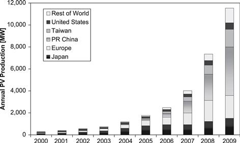
Since 1988, world wide solar cell production has increased from about 35 MW to 11.5 GW in 2009 or more than 340 times (Figures 1 and 2). Between 1988 and the mid 1990s, PV production exhibited a moderate growth rate of about 15%. With the introduction of the Japanese 70,000 roof programme in 1997, the growth rate more than doubled for the end of the decade. Since the introduction of the German feed-in tariff scheme for PV generated electricity in 2000, total PV production increased more than 30-fold, with annual growth rates between 40% and 80%.
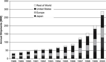
FIGURE 1 World solar cell production from 1988 to 2000 [2].
Wafer-based silicon solar cells is still the main technology and had around 80% market shares in 2009, but thin-film solar cells are continuously increasing their share since 2005. Back then, production of thin-film solar modules reached for the first time more than 100 MW per annum. Since then, the Compound Annual Growth Rate (CAGR) of thin-film solar module production was even beyond that of the overall industry, increasing the market share of thin-film products from 6% in 2005 to 10% in 2007 and 16–20% in 2009.
Amongst the different thin film technologies, the family of chalcopyrites has so far demonstrated the highest efficiency for solar cells in the laboratory as well as in production. This review gives an overview of the long-term R&D efforts to realise this as well as the industry activities to commercialise chalcopyrite solar cells. The specific details of research for chalcopyrite solar cells will be left to the specialised Chapter Ic-3.
2 Research Directions
The chalcopyrite compound family has two subclasses, which are based on the use of elements from group I, III, and VI or II, IV, and V of the periodic table and are derived from the III–V and II–VI compounds, respectively. The first ternary semiconductor device was already made in the 1920s. It was a point-contact diode made out of a mineral chalcopyrite (CuFeS2) [6]. In the early 1950s the search for new semiconductor materials led to investigations of the first III–V materials focused on finding materials with a high carrier mobility and an amphoteric doping [7,8]. Soon the search was broadened to ternary compounds and the artificial synthesis of the two subgroup families led to intensive studies of their physical properties [9–12]. In the 1960s and 70’s electrical, optical and structural properties of the (Cu,Ag)(Al,Ga,In)(S,Se,Te)2 as well as the (Zn,Cd)(Si,Ge,Sn)(P,As)2 family were investigated [13–15].
The large number of the ternary compounds and their corresponding variety of properties like the variation of band-gaps ranging from 0.26 eV (CdSnAs2) to 3.5 eV (CuAlS2), the possibility to substitute certain elements like In by Ga or Se by S, as well as the possibility to synthesise the material n- or p-type, resulted in the development of a number of novel devices at the end of the 1960s and early 1970s [14,16,17].
Initially they were explored for their non-linear optical properties [14]. Chalcopyrites were investigated with respect to their use a frequency mixing devices like the parametric oscillator, harmonic generator as well as up and down converters. Frequency mixing materials are ZnGeP2, CdGeAs2, AgGaS2, AgGaSe2, ZnSiAs2, AgGaTe2, and Proustite (Ag3AsS3) [18]. Another non-linear optical device application investigated was the use of chalcopyrites as electro-optic modulators.
The fact that a large number of chalcopyrites exhibit direct bandgaps and relatively narrow luminescent bands (sometimes at low temperatures only) made them an interesting candidate to obtain stimulated emission/laser action. It could be demonstrated that stimulated emission could be achieved in six of the ternary compounds by brute force pumping with either a high-voltage electron beam [19,20] or laser pumping [21–23]. The chalcopyrites in question were CdSiAs2, CdSnP2, CdSnP2:Ag, CuGaS2, AgGaS2, and AgGaSe2.
The ability of some of the ternary compounds to be synthesised with both n- and p-type conduction and a low resistivity was used to form the first homojunctions in CdSnP2 [24], CuInS2 [23], and CuInSe2 [25] by dopant diffusion or stoichiometry variation and vapour annealing. The stoichiometry variation and vapour anneal technique was used to produce the first ternary homodiode, which could be characterised in detail [26]. A n-type CuInSe2 crystal was treated with a short annealing in Se vapour to make a junction a short distance below the crystal surface. Then the crystal was etched to a mesa structure. For ±1 V a rectification ratio of 300:1 was obtained. Electroluminescence could be obtained with a forward bias centred on 1.34 μm and with 10% internal quantum efficiency at 77 K.
The first ternary heterodiode was reported in 1970 based on a n-type CdSnP2 single crystal combined with p-type Cu2S [27]. Despite a lattice mismatch of around 5% the device exhibited a large photovoltaic response under white light illumination. The focus of investigations changed after the first CuInSe2/CdS solar cell device with 12.5% efficiency was produced at the Bell Laboratories in 1974 [28]. This device was based on a p-type CuInSe2 single crystal onto which a thin n-type CdS layer was deposited. The result was outstanding at the time and by far better than the results achieved with thin film devices, which at that time reached around 6% [29,30]. Until the early 1980s there was a limited interest in this type of solar cell [31,32] until the first polycrystalline CuInSe2 thin-film solar cell with an efficiency of 9.4% was made in 1980 [33].
The fact that the representatives of the Cu(In,Ga)(S,Se)2 family have different bandgaps ranging from 1.04 eV (CuInSe2) over 1.54 eV (CuInS2) to 1.68 eV for CuGaSe2 and that the band-gaps can be engineered by substituting In with Ga and Se with S led to the development of Cu(In,Ga)Se2 or Cu(In,Ga)(S,Se)2 with slightly higher band-gaps of around 1.2 eV. This increase in the band-gap enhanced the voltage performance for this heterojunction solar cell.
In the early 1980s significant progress was made when the Boeing group invented the bilayer process, where a Cu-rich and In-rich layer of CuInSe2 is deposited sequentially [34]. The process was to co-evaporate Cu, In, and Se onto a molybdenum-coated glass substrate. The In-rich layer close to the heterojunction interface prevented the formation of copper nodules. In addition, the Boeing group increased the band-gap of the window layer by using CdxZn1−xS instead of CdS and Cu(In,Ga) Se2 instead of CuInSe2 which led to the then record efficiency of 14.6%. During this time the EUROCIS activities, a series of EU-funded projects, started in Europe. In August 2010 the Centre for Solar and Hydrogen Research in Stuttgart, Germany (ZSW), reported the latest world record of a 20.3% efficient Cu(In,Ga)Se2 small, area solar cell, a further increase from the 20.1% reported earlier that year [35].
In the following years research activities focused on the increase of small size solar cell efficiencies as well as on the up-scaling of the active solar cell areas in order to move the system to a production stage.
Despite a wide range of production methods, there are three methods which have dominated both research and large-scale production:
The first method was used by Mickelson and Chen [33], in 1981 to produce the first 10% all-thin-film cell based on the use of CuInSe2. The second method was initiated by Basol and Kapur in 1989 [36]. The third method was developed at Newcastle Polytechnic, now Northumbria University, by Carter et al. [37].
Over the years, many groups across the world have developed CIGS solar cells with efficiencies in the range 15–19%, depending on different growth procedures. The most commonly used substrate is glass, but significant efforts are being made to develop flexible solar cells on polyimide [38–46] and metal foils [47–59]. Highest efficiencies of 17.6%, 17.7%, and 17.9% have been reported for CIGS cells on polyimide [60], ceramics, [61] and metal foils [55], respectively.
Besides the research activities focusing on the understanding of the fundamental material and device properties and the industrialisation of Cu(In,Ga)Se2 or Cu(In,Ga)(S,Se)2, the compound family was investigated for using different members either for multijunction solar cell concepts (e.g., CuGaSe2) and concentrator concepts (single and tandem). The highest concentrator efficiency was reported in 2002 with 21.5%, but the result was recalibrated to 21.8±1.5% in the efficiency tables [62]. The first concepts end experimental result of thin-film tandem solar cells based on CuInSe2 in combination with CuGaSe2 or (CdHg)Te were presented as early as 1985 [63,64]. A combination of thin-film silicon and CuInSe2 4-terminal tandem cell (4 cm2) with 15.6% efficiency and a 30-×30-cm2 module with 12.3% aperture efficiency were reported as early as 1988 [65].
Another rather recent approach for the development of a multijunction device is the application of a dye sensitised cell (DSC) on top of the CIGS. In 2006 an efficiency of 15.09% was reported for a DSC/CIGS two terminal device [66].
CuInS2 has a direct band-gap of 1.54 eV, near the optimum for solar energy conversion. Research activities on this material for photovoltaic applications already started in the late 1970s, when a photoelectrochemical cell with about 3% efficiency was realised [67]. Early works on CuInS2 solar cells included the formation of two-source evaporated thin-film homojunctions with 3.3–3.6% efficiency [68] as well as heterojunctions with sprayed tin oxide/CuInS2[69,70] and sprayed (ZnCd)S/CuInS2 [71] with 2.0% to 2.9% efficiency.
In 1986 a 9.7% electrochemical solar cell using a n-type CuInS2 crystal was realised at the Hahn-Meitner-Institute in Berlin using a I−/I3−T-HCl redox electrolyte [72]. This was a first proof that the material could be used as a good solar cell absorber material.
The next step was to realise this efficiency with CuInS2 thin films. In 1988 a 7.3% efficient ZnO/thin CdS/CuInS2 cell was reported [73], and the first CuInS2 thin-film solar cell exceeding 10% followed in 1993 [74]. The record efficiency of CunS2 was reported with 11.4% in 2001 [75], and a further increase in efficiency was due to the widening of the band gap by adding Ga resulting in Cu(In,Ga)S2 with 12.9% efficiency [76].
One of the latest developments is the investigation of chalcopyrites as material for thin-film intermediate solar cells [77].
3 Industrialisation
The early days of PV manufacturing were dominated by investments or buy-outs of the big oil companies in small start-up or research and development companies, and with this move they took control of the research and patents. Therefore, it is no surprise that already from very early on scientific findings in the field of chalcopyrite solar cells were protected by patents as early as 1982. Table 1 gives an overview on the early US patents covering chalcopyrite solar cells.
TABLE 1 Early US Patents on CIS

As already mentioned earlier, the first CuInSe2 solar cell with 9.4% efficiency was made by the Boeing research lab [33]. The patents held by Boeing made it clear that they were active in the field of space applications. They actively participated in the Polycrystalline Thin-Film Programme at the National Renewable Energy Laboratory (NREL), formerly the Solar Energy Research Institute, but did not move beyond mini-modules into a terrestrial module manufacturing stage.
Despite the fact that Matsushita Electric and Yazaki Corporation were quite active to develop CIS solar cells in the 1990s and earlier this decade, no manufacturing activities emerged. However, it is interesting to note that despite the fact that the number of patents filed in the second half of the last decade has increased sharply, these two companies still hold the largest number of patents in this field followed by Shell and Fujielectric. Since 1985 about 10% of all patens filed in the field of thin film solar cells deal with the chalcopyrite compounds CIS/CIGS.
The Atlantic Richfield Company (ARCO) was one of the early movers to work on the commercialisation of CIS solar modules for terrestrial applications. The research work at the company to develop the CIS module technology to take advantage of CIS cell performance resulted in the achievement of a 30-×30-cm2 module with an aperture efficiency of 11.7% by 1988 [83]. In 1987 Arco Solar started to co-operate with Siemens Solar in the field of thin film solar cells (a-Si and CIS) and in February 1989 Siemens Solar completely takes over Arco Solar. Already in 1991, the company could present stability data of their mini-modules obtained by outdoor exposure testing for over 1000 days and accelerated lifetime testing [84].
Despite the promising results reported by Siemens Solar in 2001, it took another 6 years until the first commercial 5 and 10 W modules were available on the market in 1997. An expansion of the product portfolio to 20- to 40-W modules took place in 1998. At that stage a 3 MW pilot plant was operational.
In 1994 about 80 companies with a total production capacity of 130 MW existed worldwide and their activities ranged from research to production of solar cells. About half of them were actually manufacturing. Another 29 companies were involved in module production only. Out of the solar cell companies, 41 companies used crystalline silicon, 2 ribbon silicon, 19 amorphous silicon, 3 CdTe, 5 CIS (of which one was in Europe), and 10 companies worked on other concepts like III–V concentrator cells or spherical cells.
Since then, the total number of PV companies has increased manifold, and more than 300 companies with more than 450 manufacturing plants with a total 2010 production capacity exceeding 36, 11.5 GW thin films, were announced worldwide [1].
More than 200 companies are involved in thin-film solar cell activities, ranging from basic R&D activities to major manufacturing activities, and over 150 of them have announced the start or increase of production. More than 100 companies are silicon based and use either amorphous silicon or an amorphous/microcrystalline silicon structure. Over 30 companies announced using Cu(In,Ga)(Se,S)2 as absorber material for their thin-film solar modules, whereas 9 companies use CdTe and 8 companies go for dye and other materials.
In 2009, a total of 166 MW of CIGSSe solar modules was manufactured worldwide, representing about 1.5% of the annual production. Compared to the announced capacity expansions in other technologies, the expansion to 3.4 GW for CIGSSe looks small, but seems realistic (Figure 3).
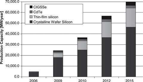
FIGURE 3 Actual and planned PV production capacities of different solar cell technologies [1].
3.1 Technology Transfer
A crucial part in the industrialisation of the Cu(In,Ga)(Se,S)2 material family for thin-film solar cells was and still is played by a number of research institutions, which do not only conduct basic material research but focus on process development and up-scaling issues as well.
Besides a larger number of university institutes, which are very active in fundamental material and/or device research there are a few research institutes, which are working on pre-pilot or pilot stage development of process steps for the commercialisation of the Cu(In,Ga)(Se,S)2 material family for thin-film solar cells. The importance of this research activities should not be underestimated as it was and is the foundation of a number of thin-film companies which are in the process of commercialisation the Cu(In,Ga)(Se,S)2 technology.
The most well-known institutes are the Ångström Solar Center, Uppsala University, Sweden; the Helmholtz Zentrum Berlin (former Hahn-Meitner-Institute), Germany; the Institute of Energy Conversion (IEC), USA; the National Institute of Advanced Industrial Science and Technology (AIST), Japan; the National Renewable Energy Laboratory (NREL), USA; and the Zentrum für Sonnenenergie- und Wasserstof-Forschung (ZSW), Germany.
3.2 Chalcopyrite Cell Production Companies
Compared with the silicon PV or the leading CdTe company, those companies manufacturing Cu(In,Ga)(S,Se)2 solar cells are still small or at an early stage, but the anticipated growth rates are significant, and it will be interesting to see how this market segment develops. The following chapter gives a short description of these companies and the basic manufacturing process they are using. This listing does not claim to be complete, especially due to the fact that the availability of information or data for some companies were very fragmentary. The given manufacturing process info are only those publicly available. The capacity, production, or shipment data are from the annual reports or financial statements of the respective companies or the cited references.
3.2.1 Ascent Solar Technologies Incorporated (USA)
The company was established in 2005 to manufacture CIGS thin-film solar modules with a roll-to-roll process. According to the company, it is on track to commence full-scale production on their 1.5 MW pilot line by the end of 2008. A 30-MW production line was completed in 2009, and it is planned to ramp up to full capacity during 2010. For 2012 the company plans to increase production capacity to 110 MW.
3.2.2 AVANCIS GmbH and Co. KG (Germany)
In 2002 Shell Solar acquired Siemens Solar including the CIS technology and continued with the development of the manufacturing technology. In 2006 Shell Solar sold the silicon production facilities to Solarworld and formed a joint venture company for the development, production, and marketing of the next generation of CIS together with Saint-Gobain called AVANCIS.
The manufacturing sequence starts with the soda-lime glass covered by a silicon nitride (SiN) alkali-barrier layer and the molybdenum (Mo) back electrode as a substrate. The first step in the CIGSSe absorber formation is the elemental precursor film deposition consisting of DC-magnetron sputtering of Cu–In–Ga:Na and thermal evaporation of selenium (Se). The second step is the reaction of the elemental precursor stack to form the CIGSSe semiconductor. Rapid thermal processing (RTP) is conducted in an infrared heated furnace capable of high heating rates in a sulphur containing ambient. The CdS buffer layer is deposited in a chemical bath deposition process, the ZnO:Al window layer by magnetron sputtering [85].
In 2008 commercial production started in the new factory with an initial annual capacity of 20 MW in Torgau, Germany. In 2009 Saint-Gobain took over the shares of Shell and started the construction of a second CIS factory with a total capacity of 100 MW in Torgau. Production in 2009 is estimated at 15 MW.
3.2.3 DayStar Technologies (USA)
The company was founded in 1997 and conducted an Initial Public Offering in February of 2004. Products are LightFoil™ and TerraFoil™ thin-film solar cells based on CIGS. In addition, DayStar has its patented ConcentraTIR™ (Total Internal Reflection) PV module, which has been designed to incorporate a variety of cell material components, including wafer-Si, Spheral Si, thin-film CIGS, and a-Si.
3.2.4 Global Solar Energy Inc. (USA, Germany)
GSE is located in Tucson and was established in 1996. In 2006, German module manufacturer, SOLON AG, acquired a 19% stake in Global Solar Energy Inc. The remaining 81% are owned by an European venture capital investor. The company is producing thin-film photovoltaic CIGS solar cells for use in solar products, as well as installing and managing large solar photovoltaic systems.
A molybdenum back contact layer is deposited onto the stainless steel film by means of sputtering. All the steps follow a roll-to-roll procedure. Copper, indium, gallium, and selenium raw materials are deposited by means of vaporisation sources whose design is primarily a result of proprietary know-how. A very thin buffer layer is then applied onto the CIGS layer. The top layer of the solar cell is a transparent but conductive layer, which is sputtered.
According to the company, the new 40-MW plant was opened in March 2008 and 35-MW plant in Germany opened in the autumn of 2008. GSE aims for 175-MW production capacity in 2010 [86]. In 2009, about 20-MW production was estimated.
3.2.5 Honda Soltec Co. Ltd. (Japan)
Honda R&D Co. Ltd. developed a CIGS thin-film module with a power output of 112 W. To commercialise the product, Honda Soltec Co. Ltd was established on 1 December 2006. Since June 2007, the company has been selling 125-W modules produced by Honda Engineering Co. Ltd. and announced that the mass production at the Kumamoto Plant, with an annual capacity of 27.5 MW, started its production in November 2007 [87].
3.2.6 International Solar Electric Technology (USA)
In 1985 the company was established in California. Since then ISET has conducted advanced technology R&D on Copper Indium Gallium Selenide (CIGS) solar cells. In 2006 ISET began with the development of a production facility for manufacturing printed CIGS photovoltaic modules. Current annual pilot plant manufacturing capacity is given with 3 MW and according to the company an expansion to 30 MW is in the planning stage.
3.2.7 Jenn Feng New Energy (Taiwan)
The company belongs to the Jenn Feng Group, an industry group which manufactures power tools, HID lights, LED lights, and solar modules based on silicon and CIGS. In addition, the company manufactures production lines for CIGS. The company developed its own nano-particle “Chemical Wet Process” for CIGS absorb layer deposition. According to the company the first production line with 30-MW capacity started mass production in December 2009, and an expansion with a second line is planned for 2010.
3.2.8 Johanna Solar Technology GmbH (Germany)
In June 2006 the company started to build a factory for copper indium gallium sulphur selenide (CIGSSE) thin-film technology in Brandenburg/Havel, Germany. The technology was developed by Prof. Vivian Alberts at the University of Johannesburg. The molybdenum back contact is deposited by DC-magnetron sputtering. After the first of three scribing steps for integrated series connection of the cells several alternating layers of a copper–gallium alloy and elemental indium are DC-magnetron sputtered. This precursor layer stack is exposed to a reactive atmosphere in which the absorber is formed [88].
The company built up a production line with a nominal capacity of 30 MW. In March 2008 the company granted a licence to the Chinese company Shandong Sunvim Solar Technology Co. Ltd. for the construction of a thin-film solar module production plant. In November 2008 the solar cell production started and in August 2009, the Robert Bosch GmbH purchased the company.
3.2.9 Miasolé (USA)
The company was formed in 2001 and produces flexible CIGS solar cells on a continuous, roll-to-roll production line. The company has installed two 20 MW production lines in its Santa Clara facility. In January 2010, the company announced that it installed a second 20-MW line and another 60-MW are planned, bringing the total capacity to 100 MW at the end of 2010 [89].
3.2.10 Nanosolar (USA)
The company was founded in 2001 and is based in Palo Alto. It is a privately held company with financial-backing of private-technology-investors. According to the company, Nanosolar developed nanotechnology and high-yield high-throughput process technology for a proven thin-film solar device technology based on GIGS. The company made headlines when it announced on 21 June 2006 that it has secured $100 million in funding and intends to build a 430 MW thin-film factory [90]. In September 2009 the company announce the completion of its European 640 MW panel-assembly factory [91]. Production for 2009 was estimated at 12 MW.
3.2.11 Odersun AG (Germany)
The company was founded in 2002 and developed a unique thin-film technology for the production of copper-indium-sulphide–based solar cells. The technology uses consecutive reel-to-reel processes. In the first process, a Cu-tape chemically cleaned followed by a variety of rinsing processes. Then indium is electrochemically deposited on the front side of the tape only. A solid Cu-In-S layer is formed by partial conversion of the In–Cu precursor into the CISCuT-absorber when the tape is exposed to reactive gaseous sulphur inside a sulphurisation reactor. Then the absorber layer surface must be treated with a KCN-solution to remove Cu2−xS from the surface before the tape is annealed. A wide-band-gap p-type CuI buffer layer is chemically deposited before a TCO stack is deposited by DC sputtering as a transparent front contact [92].
The main investor is Doughty Hanson Technology Ventures, London, and the company has signed an agreement with Advanced Technology and Materials Co. Ltd., which is listed on the Shenzhen Stock Exchange to co-operate in August 2004. The first production line was inaugurated on 19 April 2007. On 26 March 2008 the company laid the cornerstone for its 30-MW expansion project. The first 20-MW phase of this expansion was inaugurated in June 2010.
3.2.12 Shandong Sunvim Solar Technology Co., Ltd. (PRC)
The company is a subsidiary of Sunvim Group Co., Ltd. and is located in Gaomi, China. The company took a licence for manufacturing CIGSSe solar cells from Johanna Solar and its first 30-MW production line became operational in 2010. According to the company, an increase of the production capacity to 240 MW is planned without a date specified.
3.2.13 Solar Frontier (Japan)
Solar Frontier is a 100% subsidiary of Showa Shell Sekiyu K.K. In 1986 Showa Shell Sekiyuki started to import small modules for traffic signals, and started module production in Japan, co-operatively with Siemens (now Solar World). The company developed CIS solar cells and completed the construction of the first factory with 20-MW capacity in October 2006. The baseline device structure is a ZnO:B (BZO) window by a metal-organic chemical vapor deposition/Zn(O, S, OH)x buffer by a chemical bath deposition/CIS-based absorber by a sulphurisation after selenization (SAS)/Mo base electrode by a sputtering/glass substrate with three patterns for interconnections [93].
Commercial production started in FY 2007. In August 2007 the company announced the construction of a second factory with a production capacity of 60 MW to be fully operational in 2009 [94]. In July 2008 the company announced to open a research centre “to strengthen research on CIS solar powered cell technology, and to start collaborative research on mass production technology of the solar modules with Ulvac, Inc.” [95]. The aim of this project is to start a new plant in 2011 with a capacity of 900 MW. In 2010 the company changed its name to Solar Frontier, and production was given with 43 MW [96].
3.2.14 Solarion AG (Germany)
In 2000 the company was founded as a spin-off the Institute for Surface Modification (IOM) in Leipzig, Germany, with the aim to produce flexible CIGS solar cells. On a flexible polyimide web a molybdenum layer is sputtered. Then the elements Cu, In, and Ga are coevaporated, and Selenium is supplied by an ion beam source. A CdS buffer layer is deposited using chemical bath deposition and i-ZnO and ZnO:Al layers are sputter on the web as front contact [97].
In 2003 the company starts with the construction of the roll-to-roll pilot plant and the transfer of the laboratory process into an industrial roll-to-roll technology, which results in the manufacturing of first modules in 2009. According to the company they are in the planning stage for an industrial-scale manufacturing plant for flexible solar cells with a production capacity greater than 20 MW per year.
3.2.15 Solibro GmbH (Germany)
The company was established in early 2007 as a joint venture between Q-Cells AG (67.5%) and the Swedish Solibro AB (32.5%). In 2009 the company became a 100% subsidiary of Q-Cells. The company develops thin-film modules based on a Copper Indium Gallium Diselenide (CIGS) technology. The CIGS layer is deposited onto a molybdenum sputter-coated glass substrate using a co-evaporation method (PVD). Then a CdS buffer layer is deposited by chemical bath deposition before a ZnO layer as front contact is deposited.
A first production line in Thalheim, Germany, with a capacity of 30 MWp, started test production in April 2008. The line was expanded to 45 MW. A second line, with 90 MW was built in 2009 and the ramp-up started in the second half of 2009 and will continue throughout 2010. Solibro produced about 14 MW in 2009.
3.2.16 Solo Power Inc. (USA)
The company was founded in 2006 and is a California-based manufacturer of thin-film solar photovoltaic cells and modules based on CIGS. The company developed its own electrochemical roll-to-roll process. In June 2009, the company received certification under ANSI/UL 1703 standard. In April 2010, NREL confirmed that flexible CIGS solar panels manufactured on Solo Power’s pilot production line have achieved aperture conversion efficiencies of 11% [98]. According to the company, current capacity is 10 MW, with an expansion of 75–100 MW in planning.
3.2.17 Solyndra (USA)
The company was founded in 2005 and produces PV modules using their proprietary cylindrical CIGS modules and thin-film technology. The company operates a state-of-the-art 300,000-square-foot factory, which would allow production of up to 100 MW. For 2009 a production of 30 MW was reported [99]. In 2010 the company announced to increase their total production capacity to 300 MW by 2011 [100].
3.2.18 Sulfurcell Solartechnik GmbH (Germany)
The company was incorporated in June 2001 to commercialise the CuInS2 technology developed at the Hahn-Meitner-Institute (now “Helmholtz-Zentrum Berlin”), Berlin and is jointly owned by its founders and investing partners. In 2004, the company set up a pilot plant to scale up the copper indium sulphide (CIS) technology developed at the Hahn-Meitner-Institut, Berlin. Molybdenum-coated soda-lime glass is used as substrate material. The absorber deposition process starts with sputtering of copper and indium precursor layers and a subsequent rapid thermal anneal (RTP) in a sulphur containing atmosphere. The absorber is completed by a window layer consisting of a CdS buffer layer and a sputtered ZnO front contact [101].
First prototypes were presented at the 20th PVSEC in Barcelona in 2005. Production of CIS modules started in December 2005 and in 2006 the company had sales of 0.2 MW. For 2007, a production increase to 1 MW and in 2008, an increase to 5 MW was planned. The first 35-MW expansion phase was completed in October 2009. The new production site can be expanded to 75 MW.
In September 2010, the company announced the production of the first CIGSe solar modules and plans to convert part of their production facilities to this new product [102].
3.2.19 Sunshine PV Corporation (Taiwan)
The company was founded in May 2007 and is a subsidiary of Solartech Energy located in Hsinchu Industrial Park. According to the company their production capacity for their 120-W modules will reach 7 MW at the end of 2010. An expansion to 90 MW is scheduled to be completed in 2013.
3.2.20 Tianjin Tai Yang Photo-Electronic Technology Co. Ltd. (PRC)
The company is a joint-stock company with integrated research and manufacturing and was founded in June 2007. The aim is to industrialise the results of the CIGS thin film solar cell research of Nankai University performed under the national “863 key project” and the “Tianjin key scientific project.”
According to the company it is foreseen to expand the 1.5-MW pilot line to a large-scale production facility in 2010 with a single line capacity of 12 MW by 2012. At the same time, a production line for flexible substrate-based CIGS thin-film solar cells will be developed, which should lead to a 100-MW production capacity.
3.2.21 Würth Solar GmbH (Germany)
Würth Solar GmbH and Co. KG was founded in 1999 with the aim of building up Europe’s first commercial production of CIS solar modules. The company is a joint venture between Würth Electronic GmbH and Co. KG and the Centre for Solar and Hydrogen Research (ZSW). Pilot production started in the second half of the year 2000, a second pilot factory followed in 2003, increasing the production capacity to 1.3 MW. The Copper Indium Selenide (CIS) thin-layer technology was perfected in a former power station to facilitate industrial-scale manufacture. The company uses a co-evaporation method to deposit the CIGSe absorber on molybdenum-coated glass.
In August 2008 the company announced the successful ramp-up of their production facilities to 30 MW [103]. For 2009 a production volume of 30 MW is estimated.
In July 2010 the company announced the exclusive licensing of their technology to Manz Automation, an equipment manufacturer, who will be offering integrated production solutions to third parties.
4 Conclusions and Outlook
Since the invention of the first CIS solar cell in 1974, the technology has come a long way with respect to efficiency increase and commercialisation.
Thin film CIGS solar cells have exceeded 20% efficiency in 2010 and are almost at the same level as polycrystalline solar cells now. The ability to combine the Cu(In,Ga)(S,Se)2 materials family internally as well as with other materials to form multijunctions leaves the pathway open to further efficiency increases, especially for concentrator concept. However, to continue this road, further fundamental research to understand the basic material properties of the respective components as well as the interface behaviours is of great importance.
Despite the current relative low market share, the future of CIGSSe manufacturing looks very promising and the anticipated production capacity of 3.4 GW by 2015 would represent about 5% of the announced total production capacity. On the other hand, such a capacity would be sufficient to supply about 10% of the then anticipated annual world market, provided that the cost structure is taking full advantage of the advantages of this thin-film technology.
According to a number of market studies, CIGSSe should benefit from the commercialisation of high throughput manufacturing technologies in the next two to three years and it is expected, that manufacturing costs could be in the range of $0.65/W to $0.55/W by 2015, with the lower end very close to the expected cost structure ($0.55/W) of the current CdTe cost market leader.
References
1. A. Jäger-Waldau, PV Status Report 2010, Office for Official Publications of the European Union, EUR 24344 EN, ISBN:978-92-79-15657-1.
2. Maycock PD, News PV. 2003; ISSN 0739–4829.
3. Mints Paula. Manufacturer shipments, capacity and competitive analysis. In: Navigant Consulting Photovoltaic Service Program. 2009/2010; Palo Alto, CA.
4. Mints Paula. The PV industry’s black swan. In: Photovoltaics World. March 2010;.
5. News PV. Greentech Media. May 2010; ISSN 0739–4829.
6. Wherry ET. Radio detector minerals. Am Mineral. 1925;10:28–31.
7. Goryunova NA, Obukhov AP. Studies on AIIIBV type (InSb, CdTe) compounds. Kiev: in: Presentation at the Seventh All-Union Conference on Properties of Semiconductors; 1950;.
8. Welker H. Über neue halbleitende Verbindungen. Z Naturforsch. 1952;7a:744–749.
9. Hahn H, Frank G, Klingler W, Meyer A-D, Störger G. Über einige ternäre Chalkogenide mit Chalcopyritestruktur. Z Anorg Allg Chem. 1953;271:153–170.
10. Goodman HL, Douglas RW. New semiconducting compounds of diamond type structure. Physica. 1954;20:1107–1109.
11. Goodman HL. A new group of compounds with diamond type (chalcopyrite) structure. Nature. 1957;179:828–829.
12. Pfister H. Kristallstruktur von ternären Verbindungen der Art AIIBIVCV. Acta Crystallogr. 1958;11:221–224.
13. Parthé E. Crystal Chemistry of Tetrahedral Structures. first ed. New York: Gordon and Breach; 1964.
14. Shay JL, Wernick JH. The science of the solid state. In: Pamplin BR, ed. New York: Pergamon Press; 1975; Ternary Chalcopyrite Semiconductors: Growth, Electronic Properties and Applications. vol. 7.
15. Pamplin BR, Kiyosawa T, Masumoto K. Ternary chalcopyrite compounds. Prog Cryst Growth Charact. 1979;1:331–387.
16. Goryunova NA. Composite Diamond-Like Semiconductors. Moscow: (R) Sowetskoje Radio; 1968.
17. Berger LI, Prochukhan VD. Ternary Diamond-Like Semiconductors. New York: Consultants Bureau; 1969.
18. Smith RC. Device applications of the ternary semiconducting compounds. J Phys. 1975;36(C3):89–99.
19. Berkovskii M, Goryunova A, Orlov VM, et al. CdSnP2 laser excited with an electron beam. Sov Phys.-Semicond. 1969;2:1027–1028.
20. Averkirvak GK, Goryunova NA, Prochukhan VD, Ryvkin SM, Serginov M, Yu G. Shreter, Stimulated recombination radiation emitted by CdSiAs2. Sov Phys.- Semicond. 1971;5:151–152.
21. Shay JL, Johnston WD, Buehler E, Wernick JH. Plasmaron coupling and laser emission in Ag-doped CdSnP2. Phys Rev Lett. 1971;27:711–714.
22. Shay JL, Schiavone LM, Buehler E, Wernick JH. Spontaneous and stimulated emission spectra of CdSnP2. J Appl Phys. 1972;43:2805–2810.
23. Shay JL, Tell B, Kasper HM. Visible stimulated emission in ternary chalcopyrite sulfides and selenides. Appl Phys Lett. 1971;19:366–368.
24. Buehler E, Wernick JH, Shay JL. The CdP2-Sn system and some properties of CdSnPz crystals. Mater Res Bull. 1971;6:303–310.
25. Parkes J, Tomlinson RD, Hampshire MJ. The fabrication of p and n type single crystals of CuInSe2. J Cryst Growth. 1973;20:315–318.
26. Migliorato P, Tell B, Shay JL, Kasper HM. Junction electroluminescence in CuInSe2. Appl Phys Lett. 1971;24:227–228.
27. Goryunova NA, Anshon AV, Kaprovich IA, Leonov EI, Orlov VM. On some properties of CdSnP2 in strong electrical field. Phys Status Solidi (a). 1970;2:K117–K120.
28. Wagner S, Shay JL, Migliorato P, Kasper HM. CuInSe2/CdS heterojunction photovoltaic detectors. Appl Phys Lett. 1974;25:434–435.
29. Kazmerski LL, Ayyagari MS, Sanborn GA, White FR. Growth and properties of vacuum deposited CuInSe2 thin films. J Vac Sci Technol. 1976;13:139–144.
30. Kazmerski LL. Ternary compound thin film solar cells. In: Holah G, ed. Ternary Compounds 1977. London: Institute of Physics; 1977;217–228.
31. Kazmerski LL, White FR, Ayyagari MS, Juang YJ, Patterson RP. Growth and characterization of thin-film compound semiconductor photovoltaic heterojunctions. J Vac Sci Technol. 1977;14:65–68.
32. Loferski JJ, Shewchun J, Roessler B, et al. Investigation of thin film cadmium sulfide/mixed copper ternary heterojunction photovoltaic cells. In: Proceedings of the 13th IEEE PVSC. 1978;190. Washington, D.C.
33. Mickelsen RA, Chen WS. Development of a 9.4% efficient thin film CuInSe2/ CdS solar cell. In: Proceedings of the 15th IEEE PVSC. 1981;800–803. Orlando.
34. Mickelsen RA, Chen WS. Polycrystalline thin film CuInSe2 solar cells. In: Proceedings of the 16th IEEE PVSC. 1982;781–784. San Diego.
35. Green MA, Emery K, Hishikawa Y, Warta W. Solar cell efficiency tables (version 36). Prog Photovolt.: Res Appl. 2010;18:346–352 (Z.S.W., Press Release, 23 August 2010.).
36. Basol BM, Kapur VJ. Deposition of CuInSe2 films by a two-stage process utilizing E-beam evaporation, IEEE Trans Electr. Dev. 1990;37:418–421.
37. Carter MJ, I’Amm I, Knowles A, Ooumous H, Hill R. Laser processing of compound semiconductor thin films for solar cell applications. In: Proceedings of the 19th IEEE Photovoltaics Specialist Conference. 1987;1275–1278. New Orleans.
38. Basol BM, Kapur VK, Leidholm CR, Halani A, Gledhill K. Flexible and light weight copper indium diselenide solar cells on polyimide substrates. Sol Energy Mater Sol Cells. 1996;43(1):93–98.
39. Tiwari AN, Krejci M, Haug F-J, Zogg H. 12.8% efficiency Cu(In,Ga)Se2 solar cell on a flexible polymer sheet. Prog Photovolt.: Res Appl. 1999;7(5):393–397.
40. Hanket GM, Singh UP, Eser E, Shafarman WN, Birkmire RW. Pilot-scale manufacture of Cu(InGa)Se2 films on a flexible polymer substrate. In: Proceedings of the 29th IEEE Photovoltaic Specialists Conference. May 2002;567–569.
41. Birkmire R, Eser E, Fields S, Shafarman W. Cu(InGa)Se2 solar cells on a flexible polymer web. Prog Photovolt.: Res Appl. 2005;13(2):141–148.
42. Ishizuka S, Hommoto H, Kido N, Hashimoto K, Yamada A, Niki S. Efficiency enhancement of Cu(In,Ga)Se2 solar cells fabricated on flexible polyimide substrates using alkali-silicate glass thin layers. Appl Phys Express. 2008;1(9):1–3.
43. Gečys P, Račiukaitis G, Gedvilas M, Selskis A. Laser structuring of thin-film solar cells on polymers. EPJ Appl Phys. 2009;46(1):12508.
44. Zhang L, He Q, Jiang W-L, Li C-J, Sun Y. Flexible Cu(In,Ga)Se2 thin-film solar cells on polyimide substrate by low-temperature deposition process. Chin Phys Lett. 2008;25(2):734–736.
45. Caballero R, Kaufmann CA, Eisenbarth T, et al. The influence of Na on low temperature growth of CIGS thin film solar cells on polyimide substrates. Thin Solid Films. 2009;517(7):2187–2190.
46. Zachmann H, Heinker S, Braun A, et al. Characterisation of Cu(In,Ga)Se2-based thin film solar cells on polyimide. Thin Solid Films. 2009;517(7):2209–2212.
47. Kessler F, Rudmann D. Technological aspects of flexible CIGS solar cells and modules. Sol Energy. 2004;77(6):685–695.
48. Satoh T, Hashimoto Y, Shimakawa S, Hayashi S, Negami T. CIGS solar cells on flexible stainless steel substrates. In: Proceedings of the Conference Record of the 28th IEEE Photovoltaic Specialists Conference. 2000;567.
49. Herz K, Kessler F, Wächter R, et al. Dielectric barriers for flexible CIGS solar modules. Thin Solid Films 403–404 2002;384–389.
50. Herrmann D, Kessler F, Herz K, et al. High-performance barrier layers for flexible CIGS thin-film solar cells on metal foils. In: Proceedings of the Materials Research Society Symposium L: Compound Semiconductor Photovoltaics, 763. 2003;287–292. San Francisco, California, USA.
51. Hollars DR, Dorn R, Paulson PD, Titus J, Zubeck R. Large area Cu(In,Ga)Se2 films and devices on flexible substrates made by sputtering In: Proceedings of the Materials Research Society Spring Meeting. San Francisco. April 2005;vol. 865:477–482 F14.34.1.
52. Otte K, Makhova L, Braun A, Konovalov I. Flexible Cu(In,Ga)Se2 thin-film solar cells for space application. Thin Solid Films 511–512 2006;613–622.
53. Ishizuka S, Yamada A, Fons P, Niki S. Flexible Cu(In,Ga)Se2 solar cells fabricated using alkali-silicate glass thin layers as an alkali source material. J Renew Sustain Energy. 2008;1:013102.
54. Wuerz R, Eicke A, Frankenfeld M, et al. CIGS thin-film solar cells on steel substrates. Thin Solid Films. 2009;517(7):2415–2418.
55. Yagioka T, Nakada T. Cd-free flexible Cu(In,Ga)Se2 thin film solar cells with ZnS (O,OH) buffer layers on Ti foils. Appl Phys Express. 2009;2(7):072201.
56. Brémaud D, Rudmann D, Kaelin M, et al. Flexible Cu(In,Ga)Se2 on Al foils and the effects of Al during chemical bath deposition. Thin Solid Films. 2007;515(15):5857–5861.
57. Ishizuka S, Yamada A, Matsubara K, Fons P, Sakurai K, Niki S. Development of high-efficiency flexible Cu(In,Ga)Se2 solar cells: a study of alkali doping effects on CIS, CIGS, and CGS using alkali-silicate glass thin layers. Curr Appl Phys. 2009;20(2 Suppl. 1):S154–S156.
58. Shi CY, Sun Y, He Q, Li FY, Zhao JC. Cu(In,Ga)Se2 solar cells on stainless-steel substrates covered with ZnO diffusion barriers. Sol Energy Mater Sol Cells. 2009;93(5):654–656.
59. Kim MS, Yun JH, Yoon KH, Ahn BT. Fabrication of flexible CIGS solar cell on stainless steel substrate by co-evaporation process. Diffusion Defect Data B 124–126 2007;73–76.
60. Chirilă A, Bloesch P, Uhl A, et al. Progress towards the development of 18% efficiency flexible CIGS solar cells on polymer film, In: Proceedings of the 25th European Photovoltaic Solar Energy Conference/5th World Conference on Photovoltaic Energy Conversion. Valencia, Spain 6–10 September 2010;3403–3405.
61. Ishizuka S, Yamada A, Matsubara K, Fons P, Sakurai K, Niki S. Alkali incorporation control in Cu(In,Ga)Se2 thin films using silicate thin layers and applications in enhancing flexible solar cell efficiency. Appl Phys Lett. 2008;93 124105-1–124105–3.
62. Ward J, Ramanathan K, Hasoon F, et al. A 21.5% efficient Cu(In,Ga)Se2 thin-film concentrator solar cell. Prog Photovolt.: Res Appl. 2002;10:41–46 M.A. Green, K. Emery, Y. Hishikawa, W. Warta, Solar cell efficiency tables (version 36), Prog. Photovolt.: Res. Appl. 18 (2010) 346–352.
63. Arndt W, Dittrich H, Pfister F, Schock HW. CuGaSe2-ZnCdS and CuInSe2 - ZnCdS thin film solar cells for tandem systems. In: Proceedings of the Sixth E.C Photovoltaic Solar Energy Conference. April 1985;260–264. London, UK, 15–19.
64. Birkmire RW, Phillips JE, DiNetta LC, Meakin JA. Thin film tandem solar cells based on CuInSe2. In: Proceedings of the Sixth European Photovoltaic Solar Energy Conference. 15–19 April 1985;270–274. London, UK.
65. Mitchell K, Eberspacher C, Ermer J, Pier D, Milla P. Copper indium diselenide photovoltaic technology. In: Proceedings of the 8th E.C Photovoltaic Solar Energy Conference, 9–13. May 1988;1578–1582. Florence, Itlay.
66. Liska P, Thampi KR, Grätzel M, et al. Nanocrystalline dye-sensitzied solar cell/copper indium gallium selenide thin-film tandem showing greater than 15% conversion efficiency. Appl Phys Lett. 2006;88:203103.
67. Robbins M, Bachmann KJ, Lambrecht VG, et al. CuInS2 liquid junction solar cells. J Electrochem Soc. 1978;125:831.
68. Kazmerski LL, Sanborn GA. CuInS2 thin film homojunction solar cells. J Appl Phys. 1977;48:3178–3180.
69. Ram PR, Thangaraj R, Sharma AK, Agnihotri OP. Totally sprayed CuInSe2/Cd (Zn)S and CuInS2/Cd(Zn)S solar cells. Solar Cells. 1985;14:123–131.
70. Tiwari AN, Pandya DK, Chopra KL. Sol Energy Mater. 1987;15:121–133.
71. Tiwari AN, Pandya DK, Chopra KL. Fabrication and analysis of all-sprayed CuInS2/ZnO solar cells. Sol Cells. 1987;22:263–273.
72. Lewerenz HJ, Goslowsky H, Husemann K-D, Fiechter S. Efficient solar energy conversion with CuInS2. Nature. 1986;321:687–688.
73. Mitchell KW, Pollock GA, Mason AV. 7.3% efficient CuInS2 solar cell. In: Proceedings of the 20th IEEE Photovoltaic Specialists Conference. September 1988;1542–1544. Las Vegas, USA, 26–30.
74. Scheer R, Walter T, Schock HW, Fearheiley ML, Lewerenz HJ. CuInS2 based thin film solar cell with 10.2% efficiency. Appl Phys Lett. 1993;63:3294–3296.
75. Siemer K, Klaer J, Luck I, Bruns J, Klenk R, Bräunig D. Efficient CuInS2 solar cells from a rapid thermal process (RTP). Sol Energy Mater Sol Cells. 2001;67:159–166.
76. Kaigawa R, Neisser A, Klenk R. M Ch., Lux-Steiner, Improved performance of thin film solar cells based on Cu(In,Ga)S2. Thin Solid Films. 2002;415:266–271.
77. Fuertes Marrón D, Martí A, Luque A. Thin-film intermediate band chalcopyrite solar cells. Thin Solid Films. 2009;517:2452–2454.
78. 15 US patents owned by The Boeing Company, Seattle, WA: US patent numbers: 4335266 (1982), RE31968 (1985), 4684761 (1987), 4703131 (1987), 4867801 (1989), 5078804 (1992), 5141564 (1991), 5261969 (1994).
79. 12 US patents owned by Atlantic Richfield Company, Los Angeles, CA: US patent numbers: 4465575 (1984); 461109 (1986), 4612411 (1986) 4638111 (1987), 4798660 (1989), 4915745 (1990), 5045409 (1991).
80. 13 US patents owned by Matsushita Electric Co., Ltd., Kadoma, Japan: US patent numbers: 4940604 (1990), 5445847 (1995), 5474622 (1995), 5500056 (1996), 5567469 (1996), 5633033 (1997), 5714391 (1998), 5725671 (1998), 5728231 (1998).
81. 14 US patents owned by Siemens Solar or other Siemens companies: US patent numbers: 5078803 (1992), 5103268 (1992), 5474939 (1995), 5512107 (1996), 5578503 (1996), 5580509 (1996), 5626688 (1997).
82. 20 US patents owned by Yazaki Corporation, Tokyo, Japan: US patent numbers: 5501786 (1996), 5695627 (1998), 5772431 (1998), 5935324 (1999), 6036822 (2000), 6207219 (2001).
83. Mitchell K, Eberspacher C, Ermer J, Pier D. Single and tandem junction CuInSe2 cell and module technology. In: Proceedings of the 20th IEEE Photovoltaic Specialists Conference. September 1988;1384–1389. Las Vegas, USA, 26–30.
84. Tarrent DE. Al R Ramos, D.R Willett, R.R Gay, CuInSe2 module environmental durability. In: Proceedings of the 22nd IEEE Photovoltaic Specialists Conference. October 1991;553–556. Las Vegas, USA, 7–11.
85. Dalibor T, Jost S, Vogt H, et al. Advanced CIGSSe device for module efficiencies above 15%. In: Proceedings of the 25th European Photovoltaic Solar Energy Conference and Exhibition/5th World Conference on Photovoltaic Energy Conversion. September 2010;2854–2857. Valencia, Spain, 6–10.
86. Global Solar Energy, Press Release, 6 March 2008.
87. Honda, Press Release. November 2007;12.
88. Probst V, Hergert F, Walther B, et al. High performance CIS modules: status of production and development at Johanna solar technology. In: Proceedings of the 24th European Photovoltaic Solar Energy Conference and Exhibition. September 2009;2455–2459. Hamburg, Germany, 21–25.
89. Miasolé, Press Release. January 2010;14.
90. Nanosolar, Press Release. June 2006;21.
91. Nanosolar, Press Release. September 2009;9.
92. Winkler M, Griesche J, Konovalov I, Penndorf J, Wienke J, Tober O. CISCuT —solar cells and modules on the basis of CuInS2 on Cu-tape, Sol. Energy. 2004;77:705–716.
93. Kushiya K, Tanaka Y, Hakuma H, et al. Interface control to enhance the fill factor over 0.70 in a large-area CIS-based thin-film PV technology. Thin Solid Films. 2009;517:2108–2110.
94. Showa Shell, Press Release. August 2007;15.
95. Showa Shell Sekiyu, Press Release 17 July 2008.
96. Ikki Osamu. PV Activities in Japan, volume 16, no. June 2010;6.
97. Scheit C, Herrnberger H, Braun A, Ehrhardt M, Zimmer K. Interconnection of flexible CIGS thin film solar cells. In: Proceedings of the 25th European Photovoltaic Solar Energy Conference and Exhibition/Fifth World Conference on Photovoltaic Energy Conversion. September 2010;3414–3417. Valencia, Spain, 6–10.
98. SoloPower, Press Release 27 (April 2010).
99. PV News May 2010; Greentech Media, 2010, ISSN 0739–4829.
100. Solyndra, Press Release 17 (June 2010).
101. Neisser A, Meeder A, Zetzsche F, et al. Manufacturing of large-area CuInS2 solar modules—from pilot to mass production. In: Proceedings of the 24th European Photovoltaic Solar Energy Conference and Exhibition, 21–25. September 2009;2460–2464. Hamburg, Germany.
102. Sulfurcell, Press Release 6 (September 2010).
103. Würth Solar GmbH, Press Release 04 August 2008.