
Chapter IC-1
Thin-Film Silicon Solar Cells1
Chapter Outline
1.1. Tandem and Multijunction Solar Cells
2. Hydrogenated Amorphous Silicon (a-Si:H) Layers
2.1. Structure of Amorphous Silicon
2.2. Gap States in Amorphous Silicon: Mobility Gap and Optical Gap
2.3. Conductivity and Doping of Amorphous Silicon
3. Hydrogenated Microcrystalline Silicon (μc-Si:H) Layers
3.1. Structure of Microcrystalline Silicon
3.2. Optical Absorption, Gap States, and Defects in Microcrystalline Silicon
3.3. Conductivities, Doping, Impurities, and Ageing in Microcrystalline Silicon
4. Functioning of Thin-Film Silicon Solar Cells with p–i–n and n–i–p Structures
4.1. Role of the Internal Electric Field
4.1.1. Formation of the Internal Electric Field in the i Layer
4.1.2. Reduction and Deformation of the Internal Electric Field in the i Layer
4.2. Recombination and Collection
4.4. Series Resistance Problems
5. Tandem and Multijunction Solar Cells
5.3. Triple-Junction Amorphous Cells with Silicon–Germanium Alloys
5.4. Microcrystalline–Amorphous or “Micromorph” Tandems
6. Module Production and Performance
6.1. Deposition of the Thin-Film Silicon Layers
6.2. Substrate Materials and Transparent Contacts
1 Introduction
Silicon thin films for solar cells are at present predominantly deposited by plasma-enhanced chemical vapour deposition (PECVD) either from silane (SiH4) or preferably from a mixture of silane and hydrogen. They are either amorphous or microcrystalline. They contain about 5% to 15% of hydrogen atoms. The hydrogen atoms are essential, as they passivate a large part of the inherent defects in these semiconductor films.
Amorphous silicon thin films were first deposited by PECVD by R.C. Chittick et al. [2]; this work was continued in a systematic manner by Walter Spear and Peter Le Comber and their research group at the University of Dundee in the 1970s. In a landmark paper published in 1975 [3] (see also [4]), they demonstrated that amorphous silicon layers deposited from silane by PECVD could be doped by adding to the plasma discharge either phosphine (PH3) to form n-type layers or diborane (B2H6) to form p-type layers: They showed that the conductivity of these thin amorphous silicon layers (which contain about 10% to 15% hydrogen) could be increased by several orders of magnitude. Their pioneering work made it possible to use hydrogenated amorphous silicon (a-Si:H) to fabricate diodes and thin-film transistors, which can be used for the active addressing matrix in liquid crystal displays. It was Dave Carlson and Chris Wronski who fabricated the first amorphous silicon solar cells at the RCA Laboratories; the first publication in 1976 described cells with an efficiency of 2% [5], this value being increased to 5% within the same year [6]. A year later, Staebler and Wronski reported [7] on a reversible photodegradation process that occurs within amorphous silicon solar cells when the latter are exposed to light during long periods (tens to hundreds of hours). This effect is called the Staebler–Wronski effect (SWE), and it is a major limitation of amorphous silicon for solar cell technology. It is due to an increase of midgap defects, which act as recombination centres. It is a reversible effect: the initial, nondegraded state can be restored by annealing at 150°C for several hours. By affecting the quality of the photoactive layer within the cell, the SWE causes the efficiency of amorphous silicon solar cells to decrease during the first months of operation. After about a thousand hours of operation, the efficiency more or less stabilizes at a lower value. This is why it is important to always specify stabilized efficiencies for amorphous silicon solar cells. In the initial phase of amorphous silicon solar cell development, it was hoped to overcome this degradation effect. So far, nobody has succeeded in fabricating amorphous silicon layers that do not show any photodegradation. However, by adding hydrogen to silane during the plasma deposition of the layers, and by increasing the deposition temperature, the photodegradation can be somewhat reduced. Furthermore, by keeping the solar cells very thin (i-layer thickness below 300 nm), one can reduce the impact of the Staebler–Wronski effect on the cell’s efficiency. An important feature of amorphous silicon solar cells, introduced also by Carlson and Wronski, is that one does not use the classical structure of a p–n diode, as in almost all other solar cells, but one uses a p–i–n diode, keeping the doped layers (p- and n-type layers) very thin and employing the i layer (i.e., an intrinsic or undoped layer) as the photogeneration layer, where the light is mainly absorbed and its energy transferred to the charge carriers (holes and electrons). There are two reasons for this: (1) the electronic quality of doped amorphous layers is very poor; they have a very high density of midgap defects or recombination centres, so that practically all carriers, which are photogenerated within the doped layers are lost through recombination; (2) within the whole i layer of a p–i–n diode an internal electric field is created that separates the photogenerated electrons and holes and helps in collecting them in the n and p layers, respectively. The internal electric field is absolutely essential for the functioning of an amorphous silicon solar cell—without this field most of the photogenerated carriers would not be collected, and, thus, the cell’s performance would be totally unsatisfactory. The theory of p–i–n diodes has not been studied to the same extent as that of classical p–n diodes, and further work is clearly called for.
Amorphous silicon solar cells at first found only “niche” applications, especially as the power source for electronic calculators. For 15 years or so, they have been increasingly used for electricity generation: they seem particularly well suited for wide applications in building-integrated photovoltaics (BIPV). One of their main advantages is that they are available in the form of monolithically integrated large-area modules (and even as flexible modules based on stainless steel or polymer substrates). Another significant advantage is that their temperature coefficient is only –0.2%/°C—i.e., less than half of that prevailing in wafer-based crystalline silicon solar cells. At present, single-junction amorphous silicon solar cells attain in the laboratory stabilized efficiencies of more than 10% [8], whereas single-junction commercial modules have stabilized total-area efficiencies between 6% and 7%.
Microcrystalline silicon thin films containing hydrogen (μc-Si:H films) were first described in detail by S. Veprek and co-workers [9], who used a chemical transport technique to fabricate them. The first report of depositing μc-Si:H films with PECVD, from a plasma of silane strongly diluted with hydrogen, was published by Usui and Kikuchi in 1979 [10]. The plasma-deposition techniques for microcrystalline silicon layers were extensively investigated during the following years—in all cases, one obtains μc-Si:H instead of a-Si:H by increasing the hydrogen-to-silane ratio in the gas fed into the plasma. The first solar cells using μc-Si:H films as photogeneration layers (i layers) were reported in the early 1990s [11–13]. In 1994, the Neuchâtel group published solar cell results with efficiencies of more than 4% and showed that these cells had virtually no photodegradation at all [14]. By reducing the oxygen contamination in the intrinsic μc-Si:H layers, the Neuchâtel group was able to enhance the efficiency of small-area laboratory cells to more than 7% in 1996 [15–16]. After that, many other research groups started optimizing microcrystalline silicon solar cells. Plasma-deposited μc-Si:H solar cells generally also use the p–i–n configuration, just like a-Si:H solar cells, although doped microcrystalline silicon layers (p- and n-type layers) have much better electronic quality (and much higher conductivities) than doped amorphous silicon layers. Such doped microcrystalline silicon layers could basically be used as photogeneration layers. However, the use of the p–i–n configuration is still necessary in order to reduce recombination and collect the charge carriers with the help of the internal electric field within the i layer, which here again plays a key role. Because of the low optical absorption coefficient of microcrystalline silicon, the i layer of μc-Si:H solar cells has to be kept relatively thick (1 to 2 μm). At present, the best single-junction microcrystalline silicon solar cells attain stabilized efficiencies in the laboratory around 10% [17].
So far, single-junction microcrystalline silicon solar cells are not used within commercial modules. Microcrystalline silicon solar cells are, however, used as “bottom cells” within tandem cells—i.e., within microcrystalline–amorphous (so-called micromorph) tandem cells (see Section 5.4). Indeed, microcrystalline silicon, like wafer-based crystalline silicon, has a band gap around 1.1 eV and can absorb light in the near infrared range and is therefore complementary to hydrogenated amorphous silicon with its band gap around 1.75 eV, which limits light absorption to the visible range of sunlight.
Hydrogenated microcrystalline silicon (μc-Si:H), as deposited by PECVD, is not a uniform, standard material; rather, it is a mixture of crystallites, amorphous regions, and what are often referred to as “voids” or “cracks” (and which are in reality low-density regions). As we increase the hydrogen dilution in the deposition plasma, we obtain layers that are more and more crystalline and have less amorphous volume fraction and an increasing fraction of voids or cracks. The solar cells with the highest open-circuit voltage Voc, and also those with the highest conversion efficiency η, are fabricated with microcrystalline intrinsic layers having approximately 50% amorphous volume fraction and 50% crystalline volume fraction. These layers have a low density of cracks or voids and contain around 6% hydrogen.
When studying μc-Si:H layers, one faces the following peculiarities and difficulties: (1) growth is strongly substrate dependent; (2) if the hydrogen-to-silane dilution ratio is kept constant, the layers start growing with a relatively high amorphous volume fraction but become more and more crystalline as they become thicker (for this reason the i layer of a μc-Si:H solar cell has to be grown with a variable hydrogen-to-silane dilution ratio—e.g., see [18]); (3) μc-Si:H layers and cells are much more sensitive to oxygen and other impurities than a-Si:H layers and cells; and (4) individual μc-Si:H layers (especially those with a high crystalline volume fraction) often show, during storage, degradation effects even in the dark [19], these being probably due to adsorption of oxygen and to oxidation; nitrogen possibly also plays a role in this ageing process. These degradation effects are less pronounced in cells and can be avoided by storing the layers in vacuum or in an inert gas.
Finally, we may mention here that instead of using the term microcrystalline, many scientists and engineers use the term nanocrystalline to describe very the same layers and cells. The reason is the following: within μc-Si:H, the smallest features—i.e., the individual crystallites (grains)—have indeed nanometric dimensions (around 10 to 100 nm), but they are packaged together into “conglomerates” of columnar shape with dimensions often extending for more than 1 μm. One generally assumes that it is the conglomerate boundaries and not the grain boundaries that limit transport in μc-Si:H layers and collection in μc-Si:H solar cells. In state-of-the-art μc-Si:H solar cells, the columnar conglomerates will extend through the whole i layer, right from the p layer up to the n layer, and carriers can be collected without having to cross any conglomerate boundaries. Furthermore, at the conglomerate boundaries themselves, most of the defects are passivated by the amorphous regions present there. This explains why hydrogenated microcrystalline silicon solar cells generally have excellent collection properties and allow for almost perfect collection at i-layer thicknesses up to a few μm, even though the crystallites or grains themselves are indeed very small. This is an essential difference between microcrystalline silicon solar cells and classical polycrystalline (multicrystalline) silicon solar cells; the latter only function properly for grain sizes at the mm level.
1.1 Tandem and Multijunction Solar Cells
Researchers and industries working in the field of thin-film silicon solar cells have made extensive use of the tandem and multijunction concept. Various designs have been studied and commercialized; the main designs used are the following:
1. In a simple a-Si:H/a-Si:H tandem [20], both subcells of the tandem have approximately the same band gap. The advantage of the tandem concept is that the i layers of the subcells can be made thinner for the same light absorption compared to a thicker i layer in a single-junction cell. A tandem will therefore be basically less prone to light-induced degradation (i.e., to the Staebler–Wronski effect). Stabilized module efficiencies (total area) of as much as 7.1% have been obtained with this concept by the firm SCHOTT Solar Thin Film GmbH.
2. Triple-junction cells use an amorphous silicon top subcell and middle and bottom subcells based on amorphous silicon–germanium alloys: a-Si:H/a-Si,Ge:H/a-Si,Ge:H. Here the band gaps of the individual subcells are varied (through alloying with germanium) in such a way that the solar spectrum is well covered. With a corresponding laboratory cell, a record stabilized efficiency of 13.0% was achieved [21]. The firm United Solar Ovonic sells commercial modules based on this design, with stabilized total area module efficiencies in the 6% to 7% range. The advantage of these modules is that they are flexible, because the substrate material is stainless steel.
3. Micromorph (μc-Si:H/a-Si:H) tandem cells use a microcrystalline silicon bottom cell and an amorphous silicon top cell. Here the solar spectrum is ideally shared between the two subcells [22]; furthermore, the bottom μc-Si:H subcell is not subject to light-induced degradation (SWE). Commercial modules with stabilized total-area efficiencies in the 8% to 9% range are sold at present by several companies. Moreover, various industrial research laboratories have just recently announced having obtained 10% stabilized efficiency for large-area modules (see, e.g., [23]).
On the research front, many other designs for triple-junction cells are being studied. Results have been obtained for the following designs:
At this stage, it is not clear which of these designs will be the most successful; it may well be a completely different design using a novel microcrystalline alloy for one of the subcells. Such alloys are presently being developed (e.g., see [24]).
2 Hydrogenated Amorphous Silicon (a-Si:H) Layers
2.1 Structure of Amorphous Silicon
Crystalline solids, such as monocrystalline silicon wafers, have a fully regular and periodic structure; they possess what is called both short- and long-range order. In such a crystalline silicon network (or crystalline silicon matrix as it is also called), each silicon atom is bonded to four neighbouring silicon atoms. The bond angle—i.e., the angle between two adjacent bonds—is fixed at a value of 109° 28′ and remains the same throughout the whole crystalline network. Figure 1 schematically shows this situation. The bond length, or distance between two neighbouring silicon atoms within such a network, is also fixed and remains constant throughout the whole network at a value of approximately 0.235 nm.

FIGURE 1 Atomic model for a silicon atom within a crystalline silicon network, indicating the bond angle formed between two adjacent bonds. In amorphous silicon, this angle has a distribution of values.
(Reproduced from [1] with permission of the EPFL Press.)
In amorphous silicon thin films, both the bond angles and the bond lengths vary in a random fashion: there is a whole distribution of values. For instance, the bond angles have a random distribution centred around 109° 28′ and a standard deviation of 6° to 9°. If the amorphous silicon layer has just a low “amount of disorder,” then the distributions for bond angles and bond lengths will be very narrow. In this case, we will obtain “device quality” amorphous layers with satisfactory electronic properties. If the amorphous layer has a “high amount of disorder,” we will obtain broad distributions and unsatisfactory electronic properties. The disorder will directly affect the band tail states: the band tails will be more pronounced for strongly disordered layers. Amorphous silicon layers possess some amount of short-range order, the nearest atomic neighbours being in almost the same positions as would be the case for crystalline silicon. However there is no long-range order at all. Furthermore, due to the disorder prevailing in the network, about one in every 104 silicon atoms is unable to have four regular bonds with neighbouring silicon atoms; it has a broken or “dangling” bond as it is called (Figure 2(a)). These dangling bonds give rise to “midgap states” that act as recombination centres. In hydrogenated amorphous silicon, most (but not all) dangling bonds are “passivated” by a hydrogen atom (Figure 2(b)); in this case, they no longer contribute to the midgap states and do not at all act as recombination centres. The density of remaining, unpassivated dangling bonds in device-quality hydrogenated amorphous silicon (a-Si:H) is somewhere between 1014 and 1017 cm−3. (The value 1014 dangling bonds per cm3 refers to the bulk of the very best a-Si:H layers in the as-deposited or annealed state—i.e., before light-induced degradation or after its removal by annealing; the value 1017 dangling bonds per cm3 refers to a-Si:H layers after light-induced degradation.) Under the influence of light shining on the amorphous silicon layer, a degradation effect takes place that is characterized by an increase of unpassivated dangling bonds; this is the Staebler–Wronski effect. After about 1000 hours of light exposure (with light intensity equivalent to full sunlight), the dangling bond density tends to saturate at a higher value. If there are many silicon atoms with two hydrogen atoms passivating a broken bond (so-called SiH2 configuration, Figure 2(c)); it will be relatively easy to break the Si-H bonds and the SWE will be more pronounced. This is seen in porous layers, having a relatively high density of microvoids; a typical microvoid is schematically represented in Figure 3.
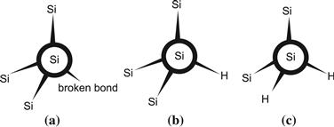
FIGURE 2 Atomic models showing (a) silicon atom with “broken bond” or “dangling bond,” (b) silicon atom with hydrogen atom passivating what was originally a broken bond, and (c) silicon atom with two hydrogen atoms, where one or both of the H atoms can easily be separated from the Si atom under the influence of light. Such an atomic configuration contributes to a pronounced light-induced degradation effect (Staebler–Wronski effect, or SWE).
(Reproduced from [1] with permission of the EPFL Press.)
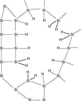
FIGURE 3 Schematic representation of a microvoid within an amorphous silicon layer, containing here four SiH2-configurations—i.e., four silicon atoms, each bonded to two hydrogen atoms. Such SiH2-configurations give very easily way to the formation of new broken bonds and thus lead to enhanced light-induced degradation.
(Reproduced from [1] with permission of the EPFL Press.)
In general, one can consider that in amorphous silicon layers the microstructure is an important structural property, which often may not have much effect on the initial layer properties but may strongly influence the light-induced degradation effect (SWE). This is a particularly disturbing situation, because one may have amorphous silicon layers and cells with reasonably good initial properties, which show their deficiencies only after several hundred hours of light-induced degradation. During the 1980s and 1990s, a huge amount of work was undertaken to clarify, understand, and reduce the SWE (for a summary, see [25]). In spite of this tremendous effort, there is to date still no complete understanding of the SWE. Experimentally, one has made the following observations:
1. The SWE can be reduced by the use of hydrogen dilution during the plasma deposition of a-Si:H and also by increasing the deposition temperatures.
2. Layers with a high density of microvoids tend to have an enhanced SWE. (Such layers can be identified with the help of the so-called microstructure factor, which is evaluated from Fourier transform infrared thermography (FTIR); see [26,27].
3. Layers with a high density of certain impurities, such as oxygen and possibly nitrogen (e.g., oxygen in excess of 2×10¹⁹ atoms per cm3), have an enhanced SWE.
4. Layers deposited at high deposition rates tend to exhibit enhanced SWE. For economic reasons (to obtain the highest production throughput possible), production facilities for amorphous silicon solar modules are always operated at the highest possible deposition rates; the limitation is then given by the SWE. For conventional PECVD with an excitation frequency of 13.56 MHz, deposition rates are limited to about 0.1 nm/s. Through the use of modified deposition techniques such as very high frequency (VHF) plasma deposition, with plasma excitation frequencies of 60 MHz and more, deposition rates of more than 1 nm/s have been obtained without any noteworthy increase of the SWE [28].
5. The magnitude of the SWE depends on light intensity and on the temperature of the layer during exposure to light. The higher the light intensity and the lower the temperature, the more pronounced the SWE will be.
6. Under constant illumination conditions, the SWE tends to saturate after the initial degradation phase. This tendency to saturate is more pronounced in complete silicon solar cells than in individual layers. The efficiency of these cells then stabilizes at a lower value.
In amorphous silicon solar cells, the p–i–n-configuration is used as already stated. Here the light enters into the cell generally through the p layer. For these amorphous silicon p layers, it is customary to employ amorphous alloys of silicon and carbon (a-Si,C:H). Such alloyed p layers have a higher band gap than do unalloyed a-Si:H layers [29]. They are used as so-called window layers: they absorb less light than unalloyed a-Si:H layers. Now all doped amorphous layers have a poor electronic quality and a very high density of recombination centres so that the light absorbed in the p layer is lost and does not contribute to the collected photocurrent. Therefore, it is of advantage for the solar cell if the p layer absorbs less light. If one increases the carbon content in the a-Si,C:H layer too much (more than approximately 40%), the gap does increase further (more than 2.1 eV), and the unwanted absorption further decreases, but the electrical conductivity of the layer decreases to values below 10−6 S/cm, and the layers are no longer suitable for solar cells [30].
For the photoactive i layers of tandem and multijunction solar cells, the use of amorphous alloys of silicon and germanium (a-Si,Ge:H) has been extensively studied. Such alloys have lower band gaps than unalloyed a-Si:H layers and allow the tuning of the spectrum absorbed in each subcell of the multijunction device to complementary parts of the solar spectrum [31–34]. However, if one increases the germanium content in the a-Si,Ge:H layer over a certain threshold (about 40% Ge content) one obtains (up to now) layers that have high-defect densities, especially in the “degraded” or “stabilized” state—i.e., after light-induced degradation. This is one reason why multijunction cells containing a-Si,Ge:H alloys have so far not led to substantial improvements in solar module efficiencies. Another disadvantage of using a-Si,Ge:H alloys is that germane is much more expensive than silane; this leads to higher overall costs for source gases, even though the utilisation ratio of germane is higher than that for silane. Furthermore, the global availability of germanium as a raw material is at present a reason for concern.
2.2 Gap States in Amorphous Silicon: Mobility Gap and Optical Gap
Classical crystalline semiconductors, such as wafer-based crystalline silicon, have a well-defined energy gap between the valence band and the conduction band. Within this energy gap, practically no electronic states can be seen (except for those due to impurities and crystal defects). In amorphous semiconductors, such as hydrogenated amorphous silicon (a-Si:H) and its alloys, there is a continuous band of states throughout and no actual band gap (Figure 4), though valence and conduction bands can still be identified. These bands have delocalized electronic states; this means that electrons in the conduction band and holes in the valence band can move about, albeit with much lower values of mobility than in the corresponding bands of (mono)-crystalline semiconductors. The highest energy level in the valence band is now given by the mobility edge EV; for energies E>EV, the states are localized, which means that the charge carriers are “trapped” and cannot move about freely.
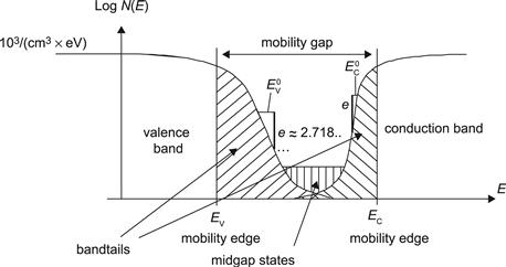
FIGURE 4 Density N(E) of electronic states for a-Si:H layers. The states within the mobility gap—i.e., between EV and EC—are localized states. The states in the valence and conduction band are delocalized or extended states, which are occupied by free holes and free electrons, respectively. The states in the valence and conduction band tails act as traps. Holes trapped within the valence band tail are in constant exchange with the free holes in the valence band; for every free hole in the valence band there are 100 to 1000 trapped holes in the valence band tail. A similar behaviour (but less pronounced) applies to electrons trapped in the conduction band tail; here there are about 10 trapped electrons for each free electron. Midgap states are associated with dangling bonds; they act as recombination centres. Their density increases by two to three orders of magnitude under the influence of the Staebler–Wronski effect.
(Reproduced from [1] with permission of the EPFL Press.)
For energies above EV, we first have the valence band tail, where the density of states N(E) decreases exponentially. Thereby, the energy constant ![]() denotes the energy needed for the exponential function to fall off by a factor of e (=2.718…). In the best device-quality a-Si:H layers,
denotes the energy needed for the exponential function to fall off by a factor of e (=2.718…). In the best device-quality a-Si:H layers, ![]() is about 45 to 50 meV.
is about 45 to 50 meV. ![]() is a measure for the disorder in the amorphous network; the higher the value of
is a measure for the disorder in the amorphous network; the higher the value of ![]() , the higher the disorder.
, the higher the disorder. ![]() can be evaluated by measuring the optical absorption coefficient as a function of photon energy (see Figure 10). Due to the capture and recombination kinetics, states in the valence band tail do not play the role of recombination centres; rather, they act as traps for the free holes during solar cell operation. One can assume that for every free hole in the valence band (i.e., for every free hole contributing to the photocurrent in the solar cell), there are 100 to 1000 “trapped” holes in the valence band tail. These trapped holes constitute a positive charge that can deform and reduce the internal electric field within the i layer of p–i–n-type solar cells.
can be evaluated by measuring the optical absorption coefficient as a function of photon energy (see Figure 10). Due to the capture and recombination kinetics, states in the valence band tail do not play the role of recombination centres; rather, they act as traps for the free holes during solar cell operation. One can assume that for every free hole in the valence band (i.e., for every free hole contributing to the photocurrent in the solar cell), there are 100 to 1000 “trapped” holes in the valence band tail. These trapped holes constitute a positive charge that can deform and reduce the internal electric field within the i layer of p–i–n-type solar cells.
Now, if the light enters into a p–i–n-type solar cell from the p side, the majority of the photogenerated holes have less far to travel than if the light enters from the n side: in the first case, they are mostly generated near the p–i interface; in the second case, they are mostly generated near the n–i interface. Thus, the field deformation through trapped charge is less pronounced in a-Si:H p–i–n-type solar cells, if the light enters from the p side: this is what is generally done.
Note that the band tails are not modified by light-induced degradation (SWE).
Above the valence band tail (for higher energies—i.e., to the right in Figure 4) we have the midgap states, given by the dangling bonds. These states act as recombination centres and are therefore detrimental to the functioning of solar cells as they directly limit the collection of the photogenerated carriers. The density of midgap states is increased by a factor of 102 to 103 by light-induced degradation (SWE).
At higher energies we can see the conduction band tail, where the density of states N(E) also follows an exponential law, but with an energy constant ![]() that is about half the value of
that is about half the value of ![]() . As the conduction band tail is much less pronounced than the valence band tail, it does not play a great role in solar cells—the electrons trapped within the conduction band tail do not noticeably deform the electric field within the i layer of p–i–n-type solar cells. (The conduction band tail does play an important role in n-channel thin-film transistors, where the electrons are the dominant charge carriers, and the density of holes is very low and of no importance at all.)
. As the conduction band tail is much less pronounced than the valence band tail, it does not play a great role in solar cells—the electrons trapped within the conduction band tail do not noticeably deform the electric field within the i layer of p–i–n-type solar cells. (The conduction band tail does play an important role in n-channel thin-film transistors, where the electrons are the dominant charge carriers, and the density of holes is very low and of no importance at all.)
A mobility edge EC separates now the localized states in the conduction band tail from the states in the conduction band with its delocalized electronic states. Instead of a “true” band gap as in (mono)-crystalline semiconductors, we now have, in amorphous silicon, a mobility gap (EC−EV), where there are the localized gap states. It is not straightforward to determine the mobility gap. It is easier to determine the so-called optical gap, a quantity that is extrapolated from measurements of the optical absorption coefficient. The optical gap is found to be about 100 meV smaller than the mobility gap [35–36].
There are different methods used for determining the optical gap. The most common method is the one proposed by Tauc et al. ([37], see also [38]). The method consists of measuring the absorption coefficient α as a function of photon energy E=hν=hc/eλ≈1.240 [eV])/(λ[μm]), for photon energies above the band gap energy. Here ν and λ are the frequency and the wavelength of light; h is Planck’s constant, c the velocity of light, e the charge of an electron (unit charge). One then plots (α(E)E)1/2 as a function of E; this plot gives us more or less a straight line (Figure 5). The intersection of this straight line with the abscissa ((α(E)E)1/2=0) gives us the value of the Tauc ga ![]() , generally used as estimate for the optical gap.
, generally used as estimate for the optical gap.

FIGURE 5 Typical plot of {α(E)E}½ versus photon energy E (with α in cm–1 and E in eV) as used for the determination of the Tauc optical gap ![]() in amorphous silicon layers.
in amorphous silicon layers.
(Reproduced from [1] with permission of the EPFL Press.)
The values measured for the optical gap in a-Si:H layers are significantly higher than are the band-gap values for crystalline silicon (c-Si); they are in the range 1.6 eV to 1.85 eV, compared to 1.1 eV for c-Si. Furthermore, the band-gap values of a-Si:H layers vary according to the deposition conditions: layers deposited at higher temperatures have lower band-gap values; layers deposited with high values of hydrogen dilution have higher band-gap values, as long as they remain amorphous and do not become microcrystalline (with a substantial crystalline volume fraction—more than 20%). In fact, if one uses high hydrogen dilution values but just avoids crossing the transition from amorphous to microcrystalline silicon, one can obtain so-called protocrystalline [39] or polymorphous [40] silicon layers that have band gaps around 1.9 to 2.0 eV, more short-range and medium-range order than do standard a-Si:H layers and a very small fraction of tiny crystallites. These layers constitute a promising topic for future research. Protocrystalline p layers are apparently used as window layers in certain amorphous silicon solar cells.
2.3 Conductivity and Doping of Amorphous Silicon
2.3.1 Conductivities
Because of its relatively high band gap, the conductivity of undoped amorphous silicon layers in the dark (without illumination) σdark is very low, between 10−8 and 10−12 (Ω−1cm−1). The value of 10−12 (Ω−1cm−1) corresponds to pure a-Si:H layers with a very low density of oxygen atoms and other impurities. Under the influence of white light of an intensity of 100 mW/cm2 (corresponding to full sunlight—i.e., to an intensity of “1 sun”) the conductivity (now called photoconductivity σphoto) increases considerably, and attains, for device quality, as-deposited (or annealed) layers values around 10−4 to 10−5 (Ω−1cm−1). The lower the density of midgap defects (or dangling bonds), the higher will be the photoconductivity σphoto. On the other hand, impurities, such as oxygen, will also, to a certain extent, increase the photoconductivity σphoto. Thus, the photosensitivity ratio (σphoto/σdark) is a measure of layer quality; it should be higher than 105 for device quality layers, even in the degraded, stabilized state.
The dark conductivity σdark of a-Si:H layers is strongly dependent on the measurement temperature. If we plot σdark in a logarithmic scale as a function of (1/T)—i.e., as a function of the inverse of the absolute temperature T—we obtain more or less a straight line. The slope of this line is Eact/k, where k is the Boltzmann constant and Eact is called the “activation energy of the dark conductivity”; it is a measure of the distance between the Fermi level EF of the layer and the nearest band edge or mobility edge. A high value of Eact means that the EF is near the middle of the mobility gap, whereas a low value means that EF is near the band edge and that the layer is strongly doped.
2.3.2 Doping
If phosphine (PH3) is fed into the PECVD deposition chamber (along with the other gases such as silane and hydrogen and possibly also methane and germane) we will obtain n-doped layers with higher dark conductivities. At the same time, the dangling bond density will also increase [41]. Similarly, if we add diborane (B2H6) or trimethlyboron (B(CH3)3) to the deposition gas mixture, we will obtain p-doped layers, also with higher dark conductivities and increased dangling bond densities. Figure 6 (adapted from [42]) shows how the Fermi level EF is shifted and the conductivity is increased by doping. Thereby, the position of EF has been evaluated by measuring the activation energy of the dark conductivity and correcting it according to the “statistical shift.” The correction due to the “statistical shift” is based on [43], Section 8.1.1, assuming a constant density for the deep states (or midgap states) of 1016/cm3eV and an exponential band tail, as shown by a full line in Figure 8.3 of [43] (E0C≈25 meV).
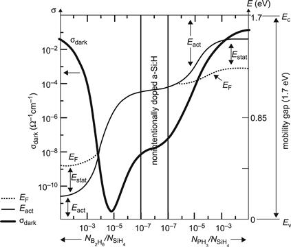
FIGURE 6 Measured values of dark conductivity σdark (full, thick line); measured values of the dark conductivity activation energy Eact (full, thin line, plotted in the figure as distance from the corresponding mobility edges EC, EV) and estimated position of the Fermi energy EF for amorphous silicon layers, produced by PECVD on glass, in function of the gas-phase doping ratio NPH3/NSiH4 (for n-type layers) and ![]() (for p-type layers). Values of σdark and Eact are from [3]. To obtain the curve for the Fermi level EF, the statistical shift has been taken into account, based on [43] (see text). The equivalent band gap of a-Si:H (or “mobility gap” as it is called here), is taken to be 1.7 eV; this corresponds to generally published values.
(for p-type layers). Values of σdark and Eact are from [3]. To obtain the curve for the Fermi level EF, the statistical shift has been taken into account, based on [43] (see text). The equivalent band gap of a-Si:H (or “mobility gap” as it is called here), is taken to be 1.7 eV; this corresponds to generally published values.
(Figure taken, with permission, from [42], as modified in [1].)
Note that it is not possible to dope a-Si:H layers in such a way that the Fermi level EF approaches the mobility edges. There remains, even for strong dopant concentrations, a distance of about 400 meV; this is caused by the effect of midgap states and band tails. Due to this difficulty in doping, the open-circuit voltage in a-Si:H solar cells is always much lower than the “theoretical” limit value it should have based on its band-gap value.
Note also that, at least in the original data published in [3] (on which Figure 6 is based), layers produced with pure silane (and without any dopant gases) have a slightly n-type character. It took here a slight p-type doping (with a gas-phase doping ratio NB2H6/NSiH4 ≈ 10−5) to obtain “truly intrinsic” layers, with a dark conductivity activation energy Eact of 0.85 eV. It is known today that this is due to unintentional doping by oxygen impurities. If the oxygen content is kept below 2×10⁻¹⁸ cm3 by using high-purity gases and other precautionary measures, then a-Si:H layers without any dopants will be “truly intrinisc” and have a dark conductivity activation energy Eact of 0.8 eV or more.
3 Hydrogenated Microcrystalline Silicon (μc-Si:H) Layers
3.1 Structure of Microcrystalline Silicon
Hydrogenated microcrystalline silicon (μc-Si:H), as deposited by PECVD from a mixture of silane and hydrogen, is a mixed-phase material containing a crystalline phase (with tiny crystallites grouped into “conglomerates” or “clusters”), an amorphous phase, and voids (which are very often not real voids but just regions with a lower density [44–45]). By varying the hydrogen dilution ratio R=[H2]/[SiH4] in the plasma deposition (where [H2] denotes the rate of hydrogen gas flow into the deposition system and [SiH4] the rate of silane gas flow), one can obtain many different types of layers: (a) at low hydrogen dilution—i.e., at low values of R, amorphous layers; (b) by slightly increasing R, layers with mainly an amorphous phase and a low concentration of very tiny crystallites (such as protocrystalline silicon layers); (c) at still higher hydrogen dilution, layers with about 50% amorphous phase and 50% crystalline phase; and (d) at very high values of R, highly crystalline layers, which tend to have a large concentration of cracks or voids and thus constitute low-density, porous material.
When deposited on a glass substrate, the μc-Si:H layers usually start off with an amorphous incubation phase and the nucleation of crystallites only begins later on. This is shown schematically in Figure 7 [46]. Within μc-Si:H solar cells, the situation is more complex, as the μc-Si:H intrinsic layer is deposited on a p-doped or an n-doped microcrystalline layer, and the latter on a rough substrate. One strives, in fact, to avoid the formation of an amorphous incubation layer (which leads to a reduction in solar cell performance) by starting off the deposition with a relatively high value of R. The value of R at which microcrystalline growth starts depends very much on the deposition parameters, such as plasma excitation frequency, substrate temperature, and deposition pressure. The values of R indicated in Figure 7 are merely given as an example and are typical of deposition at relatively high pressures (2 to 3 Torr), with a plasma excitation frequency of 13.56 MHz.
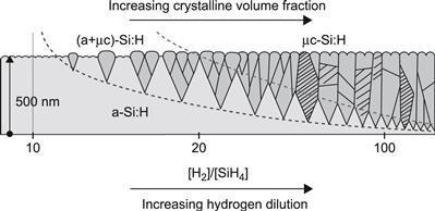
FIGURE 7 Range of film structures (schematic), obtained with different PECVD parameters, for films deposited on glass substrates; the dashed lines indicate the transitions between amorphous and mixed phase material, as well as between mixed phase material and highly crystalline material.
(Reproduced with permission from [46], in the form as published in [1].)
It is generally assumed today that most of the defects (i.e., most of the recombination centres) in μc-Si:H are located at the boundaries of the conglomerates or clusters. It is also assumed that these defects are passivated by the amorphous phase. For this reason, one uses, as intrinsic layers within p–i–n- or n–i–p-type μc-Si:H solar cells, layers with about 50% crystalline volume fraction.
Let us take a closer look at the microstructure of a typical μc-Si:H layer. Figure 8 shows part of a μc-Si:H layer taken as a high-resolution transmission electron microscopic (TEM) image within a conglomerate of silicon crystallites: the latter have diameters between 10 and 20 nm and are embedded into an amorphous silicon matrix. The conglomerates themselves are separated by a varying amount of amorphous silicon, cracks and voids, and low-density material [47]. The microstructure is highly complex. In addition, the μc-Si:H layer is neither uniform nor anisotropic, because the conglomerates form cones that widen up toward the top of the layer until they touch each other as schematized in Figure 7.
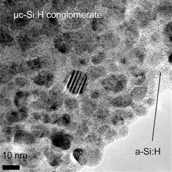
FIGURE 8 High-resolution TEM micrograph of a plane view taken within a microcrystalline conglomerate. Spherical nanocrystals (one of them highlighted) are embedded in amorphous tissue and constitute the microcrystalline phase itself.
(Reproduced with permission from [47].)
The most convenient way to assess the “crystallinity” of μc-Si:H layers is to use Raman spectroscopy. With this technique, one investigates the local atom–atom bonding structure of a material by studying the interaction of monochromatic incoming light (photons of a given energy) with the bond vibrations in the material (phonons). The energy of the incoming photons is shifted by the energy of the phonon involved in the interaction. Due to scattering of light, one is able to collect and analyse the outgoing photons with the energy shifts. The amplitude of the scattered light is measured as a function of the shift in photon energy: this constitutes the Raman spectrum. Thereby, a unit called wavenumber is used, which is simply the reciprocal of wavelength and is expressed in cm−1. The conversion between photon energy E, wavelength ![]() , and wavenumber ν is
, and wavenumber ν is ![]() . Crystalline silicon has a narrow peak in its Raman spectrum at 520 cm−1 and, due to defective regions, a tail around 500 to 510 cm−1 wavenumbers, whereas amorphous silicon exhibits a broad Raman signal centred at 480 cm−1[48]. By suitably analysing the Raman spectrum, one finds the total signal intensity Ic due to crystalline contributions and the total signal intensity Ia due to the amorphous contribution. The ratio Ic/(Ic+Ia) is a semiquantitative indication for the crystalline volume fraction and is called Raman crystallinity. It is rather difficult and cumbersome to evaluate the actual crystalline volume fraction (this can be done, e.g., by a high-resolution TEM but requires the attribution of the various regions in the layer to the crystalline and amorphous phases, which is not an easy task). Therefore, the value of the Raman crystallinity is generally used for μc-Si:H layer optimization in connection with solar cells. The best solar cells are obtained for values of Raman crystallinity around 50% to 60%.
. Crystalline silicon has a narrow peak in its Raman spectrum at 520 cm−1 and, due to defective regions, a tail around 500 to 510 cm−1 wavenumbers, whereas amorphous silicon exhibits a broad Raman signal centred at 480 cm−1[48]. By suitably analysing the Raman spectrum, one finds the total signal intensity Ic due to crystalline contributions and the total signal intensity Ia due to the amorphous contribution. The ratio Ic/(Ic+Ia) is a semiquantitative indication for the crystalline volume fraction and is called Raman crystallinity. It is rather difficult and cumbersome to evaluate the actual crystalline volume fraction (this can be done, e.g., by a high-resolution TEM but requires the attribution of the various regions in the layer to the crystalline and amorphous phases, which is not an easy task). Therefore, the value of the Raman crystallinity is generally used for μc-Si:H layer optimization in connection with solar cells. The best solar cells are obtained for values of Raman crystallinity around 50% to 60%.
3.2 Optical Absorption, Gap States, and Defects in Microcrystalline Silicon
Compared with intrinsic a-Si:H layers, intrinsic μc-Si:H layers show the following striking differences.
1. Lower optical band gap (1.1 eV, similar to the band gap of crystalline silicon) is associated with the crystalline phase of the material [49].
2. Band tails are less pronounced than in a-Si:H; one may assign a value of about 30 meV to the exponential fall-off constant ![]() of the valence band tail [50]. The fact that the valence band tail is less pronounced in intrinsic μc-Si:H layers than in intrinsic a-Si:H layers is probably the reason why μc-Si:H p–i–n-type solar cells can often be illuminated both from the p side as well as from the n side (see, e.g., [51]), resulting in both cases in similarly effective photocarrier collection.
of the valence band tail [50]. The fact that the valence band tail is less pronounced in intrinsic μc-Si:H layers than in intrinsic a-Si:H layers is probably the reason why μc-Si:H p–i–n-type solar cells can often be illuminated both from the p side as well as from the n side (see, e.g., [51]), resulting in both cases in similarly effective photocarrier collection.
3. Lower defect absorption results from midgap defects (essentially dangling bonds) [52]. The defect absorption is taken for μc-Si:H at a photon energy value of 0.8 eV [49], whereas it is taken for a-Si:H at a photon energy value of 1.2 eV. If the same calibration factor between defect absorption and defect density would apply in both materials, this would mean that the defect densities in device-quality μc-Si:H layers would be much lower than in a-Si:H layers. However, because of the mixed-phase nature of μc-Si:H layers, it is doubtful whether such a conclusion can be drawn [53]. Nevertheless, defect absorption at 0.8 eV, measured preferably by Fourier transform infrared spectroscopy (FTPS) [54] is a very convenient method for comparing the “quality” of different μc-Si:H layers, in view of their use in solar cells. The defect absorption of μc-Si:H layers has a minimum for a value of Raman crystallinity around 50% to 60%, and increases for layers with both lower and higher crystallinity. It is precisely with such layers that the solar cells with the best performances are fabricated. Figure 9 shows defect absorption (as measured by FTPS) for intrinsic μc-Si:H layers with different values of Raman crystallinity before and after degradation.
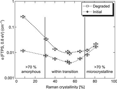
FIGURE 9 Defect absorption α, at a photon energy of 0.8 eV, measured by Fourier transform infrared spectroscopy (FTPS), before and after light soaking by a standard procedure (see text).
(Reproduced with permission from [56], © 2005 IEEE.)
4. There is a much less pronounced light-induced degradation effect [55–58]. This is best seen in complete solar cells; here, under the standard light-soaking procedure used (50°C substrate temperature, AM1.5 light at 100 mW/cm2 intensity; 1000 hours of light exposure), the relative degradation in the efficiency of μc-Si:H single-junction cells, with 0.5-μm-thick i layers, is only about 5%, whereas a-Si:H single-junction solar cells with 0.5-μm-thick i layers show more than 25% efficiency loss. The increase in defect absorption (at 0.8 eV) of μc-Si:H layers is also just about a factor 2, whereas the corresponding increase in defect absorption (at 1.2 eV) of a-Si:H layers is at least a factor 10. Note that the defect absorption of degraded μc-Si:H layers has a minimum for a value of Raman crystallinity around 50% to 60%. Layers with <30% crystallinity degrade strongly, whereas layers with more than 70% crystallinity hardly degrade at all but have very high values of defect absorption both in the initial and degraded states (see Figure 9).
5. The visible range of the light spectrum has a lower optical absorption coefficient—i.e., for photon energies between 1.65 eV and 3.2 eV (i.e. for wavelengths between 750 nm and 390 nm). As a consequence, μc-Si:H solar cells have to be much thicker than a-Si:H solar cells to usefully absorb the incoming light. The lower optical absorption results from the indirect band gap of μc-Si:H; meaning that a phonon has to be present for a photon to be absorbed due to the rule of momentum conservation. As a consequence, fewer photons are absorbed and fewer electron–hole pairs are generated. On the other hand, in a-Si:H the rule of momentum conservation is relaxed because of the random nature of the amorphous network. The absorption of photons and the photogeneration of electron–hole pairs are correspondingly increased.
Figure 10 shows the main differences in optical properties, between typical μc-Si:H layers and typical a-Si:H layers, by displaying, in a logarithmic scale, the absorption coefficient α(hν) for the applicable spectral range—i.e., for photon energies Ephoton = hν from 0.7 eV to 3.5 eV—corresponding to wavelengths from 350 nm to 1750 nm.
While interpreting Figure 10, note the following:
a. The optical band gap Eg can be evaluated by extrapolation from region A in Figure 10 (the region with high absorption coefficients). This is commonly done by the procedure according to Tauc et al., as shown in Figure 5.

FIGURE 10 Plot of absorption coefficient α versus photon energy E=hν, for device-quality a-Si:H and μc-Si:H layers, indicating the three important parameters that can be evaluated from this plot: (A) optical band gap Eg; (B) Urbach energy E0; (C) defect (dangling bond) density Ndb. The curves for a-Si:H are drawn with thick uninterrupted lines (_______); the curves for μc-Si:H with fine dashed line (- - - - - -). The curves given here are purely indicative; they do not necessarily correspond to actual a-Si:H and μc-Si:H layers as used in most R and D laboratories.
(Courtesy of Michael Stückelberger, PV Lab, IMT, EPFL, Neuchâtel.)
b. The band tails (and especially the valence band tail) can be assessed from region B, where α(hν) follows an exponential curve (which is a straight line in Figure 10, because of the logarithmic scale). The exponential decrease of α(hν)—i.e., the slope of the straight line in the logarithmic representation—is given by 1/E0, where E0 is called the Urbach energy. The Urbach energy E0 is considered in a-Si:H layers to be roughly equivalent to ![]() , whereas in μc-Si:H layers it may, in fact, depend on both
, whereas in μc-Si:H layers it may, in fact, depend on both ![]() and
and ![]() .
.
c. Region C in Figure 10 gives a qualitative indication for the density of midgap defects, which can be associated with dangling bonds. In μc-Si :H layers, it is not really clear where these dangling bonds are located; from transport measurements [47,59], one may presume that they are located at the boundaries of the conglomerates.
3.3 Conductivities, Doping, Impurities, and Ageing in Microcrystalline Silicon
3.3.1 Conductivities
Because of the lower mobility gap of the crystalline phase of μc-Si:H, the values of dark conductivity σdark are significantly higher than in a-Si:H; they are between 10−8 and 10−6 (Ω−1cm−1) for Raman crystallinities between 60% and 80%, provided we have “truly intrinsic” material with a low content of impurities [60]. The photoconductivity σphoto of such layers is only slightly higher than in a-Si:H, with values around 10−4 and 10−5 (Ω−1cm−1). The photosensitivity ratio (σphoto/σdark) can still be used as one of the criteria for layer quality. Furthermore, the dark conductivity activation energy Eact remains a convenient indication for the position of the Fermi level. For “truly intrinsic” material with a low content of impurities, Eact will be >0.5 eV. Intrinsic μc-Si :H layers with a photosensitivity ratio of 10−3, a dark conductivity activation energy >0.5 eV, and a Raman crystallinity of 50% to 60% can thus be considered good candidates for the intrinsic layers of solar cells. Figure 11 shows commonly obtained values for σdark and σphoto in function of Raman crystallinity.

FIGURE 11 Dark conductivity (filled symbols) and photoconductivity (open symbols) as a function of Raman crystallinity.
(Reproduced with permission from [60], showing typical error bars.)
3.3.2 Doping
By adding phosphine, diborane, or trimethylboron to the silane plus hydrogen gas mixture and feeding it into the deposition chamber, μc-Si:H layers can be doped in a similar way as a-Si: layers. In contrast with a-Si:H, one does not observe an additional creation of midgap defects through doping (see, e.g., [61]). As a consequence, one can push here, by doping, the Fermi level EF almost to the mobility edges EC, EV, and it does not remain some 300 to 400 meV away from them as in strongly doped a-Si:H layers (see Figure 6). The conductivities obtained thereby are also considerably higher than in a-Si:H: they are about 102 (Ω−1cm−1), rather than just 10−2 (Ω−1cm−1). As a consequence thereof, the best μc-Si:H solar cells have open-circuit voltages in excess of 600 mV [17,62,63]—i.e., not very far from the theoretical limit value as given by the band gap of the crystalline phase of μc-Si:H.
3.3.3 Impurities
Undoped μc-Si:H layers with oxygen concentrations above 1019 cm−3 in general show clear n-type behaviour. Under usual deposition conditions, it is only by reducing the oxygen concentration to 2×1018 cm−3 that “truly intrinsic” layers can be deposited, with the Fermi level EF in the middle of the gap and with dark conductivity activation energy Eact higher than 500 meV. By incorporating layers with low oxygen content as intrinsic layers (i layers) into p–i–n-type solar cells, one obtains solar cells with high efficiencies and with a broad spectral-response curve [16], as shown in Figure 12. Layers with low oxygen content are obtained, either by employing a gas purifier, as reported in [16], or by utilizing high-purity source gases. If the i layers are deposited at low temperatures (at temperatures below 180°C), the oxygen impurities apparently do not play the same active role as at higher temperatures (but are passivated by the hydrogen atoms), and solar cells with higher efficiencies have been obtained even with a relatively high oxygen contamination of 2×1019 cm−3[64,65]. On the other hand, such low-temperature deposition is currently not used to fabricate the best μc-Si:H solar cells; furthermore, it is hardly compatible with the production of “micromorph” tandems (see Section 5.4). Nitrogen impurities have a similar effect as oxygen impurities [66].
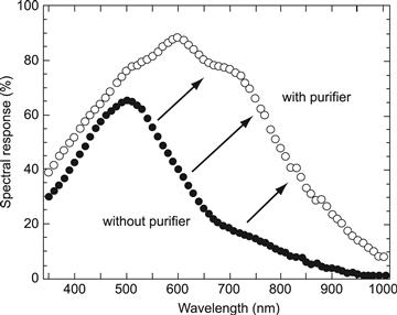
FIGURE 12 Quantum efficiency (spectral response) curve of a typical microcrystalline silicon solar cell, fabricated with and without gas purifier. In the latter case, a relatively high oxygen contamination of 1020 cm−3 leads to a strong deformation of the internal electric field within the i layer of the p–i–n-type solar cell by positively charged oxygen atoms acting as donors and thus to very poor collection.
(Reproduced with permission from [16].)
3.3.4 Ageing
Because of the porous nature of μc-Si:H layers (especially of μc-Si:H layers with high crystalline volume fraction), oxygen and other impurities can easily enter into these layers [19] (and even into entire solar cells if they are not encapsulated), provoking thereby a change in dark conductivity (and a reduction in cell performance). This ageing effect takes place in the dark and at room temperature over a period of days to months. By annealing in vacuum or inert gas for several hours at temperatures typically higher than 130°C, this effect can be reversed. The ageing effect is an additional difficulty when developing and characterizing μc-Si:H layers and solar cells.
4 Functioning of Thin-Film Silicon Solar Cells with p–i–n and n–i–p Structures
4.1 Role of the Internal Electric Field
All solar cells function according to the following two principles:
1. An electron and hole pair is generated by absorption of an incoming photon within a semiconductor; this is possible if the energy of the photon Ephoton = hν = hc/eλ is larger than the band gap of the semiconductor—i.e. if Ephoton > Eg, where Eg is the band gap of the semiconductor (taken to be somewhere between 1.6 and 1.85 eV for a-Si:H, depending upon deposition conditions, and 1.1 eV for μc-Si:H); ν and λ are the frequency and the wavelength of light, respectively; h is Planck’s constant; c the velocity of light; and e the charge of an electron (unit charge). The majority of the photons of a given wavelength λ is only absorbed if the thickness d of the semiconductor is larger than the penetration depth dpen of the photons. The penetration depth dpen becomes larger as λ is increased—i.e., as Ephoton is decreased and approaches Eg. This is especially critical for thin-film silicon solar cells, where the thickness d of the semiconductor is of the order of 1 μm. In these cells, one has to utilize special light-trapping schemes in order to absorb a sufficient part of the incoming sunlight (see Section 4.5).
2. Holes and electrons are separated by the action of an internal electric field created by a diode configuration. This can be described as follows:
a. The majority of solar cells are built as p–n diodes; here the electric field is limited to the depletion layers—i.e., to two very narrow zones at the interface between p and n regions. Photogenerated carriers travel by diffusion up to the depletion layers and are then separated by the strong electric field prevailing there. As long as the carrier diffusion lengths are sufficiently high—i.e., as long as they are much higher than the cell thickness d, the collection losses are low, and the solar cell functions properly.
b. In thin-film silicon solar cells, the diffusion lengths are, in general, very small; they are, in fact, often smaller than the thickness d of the solar cell. Thus, diffusion alone is not sufficient to ensure transport and collection of the photogenerated carriers. One therefore utilizes the internal electric field to assist also in the transport of the photogenerated carriers. This is only possible with a p–i–n (or n–i–p) diode configuration: here the internal electric field extends throughout the whole i layer and governs both transport and separation of the photogenerated carriers.
Figure 13 shows a comparison for the profile of the internal electric field E(x) between p–n and p–i–n diodes. Note that for zero external (applied) voltage V, the integral ∫ Eint(x)dx is, for both types of diodes equal to the built-in voltage Vbi, a parameter, which is approximately equal to 1 Volt, for all forms of silicon. If V≠0, one can write: V=∫−Eext(x)dx; this means that if the applied voltage is negative, it gives a reverse bias to the diode and the electric field is augmented (as shown in the figure); if the applied voltage is positive, it gives a forward bias to the diode and the electric field is reduced. As V approaches the open-circuit voltage Voc of the solar cell, the internal electric field becomes strongly reduced. Note that in relation to the corresponding energy gaps, Voc values of p–i–n- and n–i–p-cells are fundamentally lower than the theoretical limit values found for p–n cells.
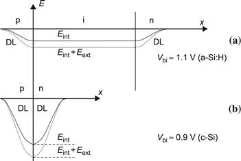
FIGURE 13 Internal electric field Eint(x), for (a) p–i–n-type and (b) p–n-type diodes; Eint is the internal electric field for zero applied voltage, Eext is the additional electric field due to an external or applied voltage V, E = Eint + Eext is the total electric field, Vbi is the built-in voltage of the diode, and DL is the depletion layer. The sign of the electric field is negative because it is directed from the n region to the p region (i.e., toward negative values of x). Thus, the electric field separates electrons and holes; it pushes the photogenerated holes toward the p region, where they are collected, and the photogenerated electrons toward the n region, where they are, in their turn, collected.
(Reproduced from [1] with permission of the EPFL Press.)
Due to the action of the internal electric field E(x) in the i layer of p–i–n- and n–i–p-type solar cells, transport (and collection) of the photogenerated carriers is now governed (as long as V is not too high) by the drift length Ldrift of both electrons and holes within the i layer. For thin-film silicon, one generally writes Ldrift=μτE, where μ is the mobility of the carrier (electron or hole), τ the lifetime, and E the magnitude of the prevailing electric field. One can consider that, for a given value of E, Ldrift will be approximately equal for both carriers (electrons and holes) [67,68]. One finds also that, at short-circuit conditions, the drift length has a value that is about 10 times higher than the minority-carrier diffusion length [69]: this is, of course, the reason, why one uses the p–i–n (or n–i–p) configuration for all a-Si:H and for most μc-Si:H. As previously stated, the minority-carrier diffusion lengths in these materials would be too small, often quite a bit smaller than the i layer thickness di.
Thus, for thin-film silicon solar cells on glass substrates, the structure shown in Figure 14 is obtained. Note that for optimal performance of a-Si:H solar cells, the light has to enter the solar cell through the p layer; it is only then that the deformation of the internal electric field through trapped charge in the valence band tail can be kept negligibly small (see Section 2.2). Therefore, if the solar cell is deposited on a substrate, which is not fully transparent (or, unlike glass, does not remain for several decades fully transparent but eventually becomes yellowish like most polymers), then the deposition sequence n–i–p is used. A textured reflector layer (e.g., textured silver) is deposited on the substrate followed by the n, i, and p layers; on top of the p layer, a transparent conductive oxide (TCO) and a grid for current collection are used. The n–i–p-configuration is regularly employed not only for solar cells deposited on stainless steel substrates but also on most polymer substrates.

FIGURE 14 Typical structure of p–i–n-type amorphous silicon solar cell on glass substrate. Microcrystalline silicon solar cells have a similar structure; however, in the latter case, the i layer is much thicker—i.e., 1 to 2 μm thick.
(Reproduced from [1] with permission of the EPFL Press.)
Although it would be feasible to let the light enter through the n side in single-junction μc-Si:H solar cells (because the trapped charge in the valence band tail is much less prominent than in a-Si:H), μc-Si:H solar cells are, in practice, almost exclusively used in tandem and multijunction structures, together with a-Si:H solar cells, so that once again one prefers to let the light enter from the p side.
Because the doped layers in thin-film silicon do not have a sufficiently high conductivity as does wafer-based crystalline silicon, a TCO layer has to be used as the contact layer adjacent to the p layer—on the side where the light enters the solar cell. In practice, the TCO layer is often textured and thus contributes to light scattering (see Section 4.5). In the case of p–i–n-type solar cells (as shown in Figure 14), the thin-film silicon layers are deposited on top of this TCO layer: the TCO layer has therefore to withstand the action of a silane plus hydrogen plasma. In this case, F-doped SnO2, Al-doped ZnO, or B-doped ZnO layers are used as TCO layers. (The SnO2 layer tends to be reduced by the hydrogen-rich plasma used for the deposition of μc-Si:H and should in this case be covered by a thin protective layer—e.g., by a thin ZnO or a thin TiO2 layer [47]). In the case of n–i–p-type solar cells, the TCO contact layer is deposited after the thin-film silicon layer and very often indium tin oxide (ITO) layers are used.
4.1.1 Formation of the Internal Electric Field in the i Layer
Thermal equilibrium in a p–i–n-diode is established by the formation of space charge regions in the p- and n-doped layers. The space charge is constituted by the ionized dopant atoms and is responsible for forming the internal electric field, as schematically drawn in Figure 15. In uniform doped p layers (without a p–i junction), the charge constituted by the negatively ionized acceptor atoms (density N−A) is neutralized by free holes (density pf) and trapped holes (density pt), as one has N−A=pf+pt and, thus, charge neutrality. Similarly, in uniform doped n layers, (without a n/i junction) the charge constituted by the positively ionized donor atoms (density N−D) is neutralized by free electrons (density nf) and trapped electrons (density nt), as one has here N+Dnf+nt, and, thus, again charge neutrality. On the other hand, when we have a p–i junction, then that part of the p layer, which is just adjacent to the i layer, will have virtually no free holes (pf ≈ 0) in the valence band, because most free holes remaining in that “frontier zone of the p layer” would immediately travel by diffusion to the i layer, where their density is very much lower; now, through the processes of capture and thermal emission, there is a constant exchange between the free holes in the valence band and the trapped holes in the valence band tail and the density pt of trapped holes can be considered roughly proportional to the density pf of free holes (see [70]). Thus, there remain in the “frontier zone of the p layer” practically only the ionized acceptor atoms, which make up a negative space charge Q, as shown in Figure 15. Similarly there remain in the “frontier zone of the n layer” practically only the ionized donor atoms, which make up a positive space charge Q. The internal electrical field extends between these two space charge regions. If we look at an ideal p–i–n-diode, then the i layer itself will not contain any significant charge contributions and the electric field will be constant; it will have (for zero applied voltage) a value Ei equal to −(Vbi/di), where di is the thickness of the i layer and Vbi is the built-in voltage of the solar cell. Vbi is essentially given by the sum of the two shifts in Fermi level EF due to doping in both the p and n layers (see [1], Figure 4.33); in amorphous silicon, the mobility gap is relatively large(≈1.7 eV), but we can only push the Fermi level EF by doping to a position, which is approximately 300 meV away from the mobility edges EC, EV so that Vbi≈1.7 eV−(2×0.3 eV)≈1.1 eV. In microcrystalline silicon, the mobility gap is smaller (≈1.1 eV), but we can push the Fermi level EF by doping to a position, which is just about 50 to 100 meV away from the mobility edges EC, EV, so that Vbi≈1.1 eV−(2×0.1 eV)≈0.9 eV. The values given here are the maximum values for Vbi and are applicable if the p and n layers are correctly doped and sufficiently thick. (In practice, this means that the doped layers should be thicker than about 10 nm; the p layer, through which the light enters the cell, must be kept especially thin, because the light that is absorbed here is generally lost and does not contribute to photogeneration. This “parasitic” absorption can be reduced even further by using a silicon–carbon alloy as p layer with a higher band gap, especially in the case of a-Si:H solar cells. The n layer, which is at the “back” of the cell, is generally made quite a bit thicker—some 20 to 25 nm thick.)
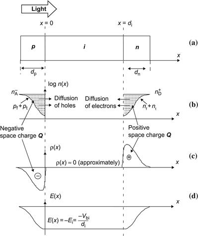
FIGURE 15 Sketch of a p–i–n-diode showing the formation of space charge Q in the “frontier zones” of the p and n layers (at the boundaries toward the i layer). In these frontier zones. the concentrations of free carriers (pf, nf) and of trapped carriers (pt, nt) are very low (the carriers diffuse away from these frontier zones into the i layer). In the p layer, we are therefore essentially left with the negatively ionized acceptor atoms (density N−A), forming a negative space charge; in the n layer, we are essentially left with the positively ionized donor atoms (density N−D), forming a positive space charge.
(Reproduced from [1] with permission of the EPFL Press.)
In order to design solar cells with satisfactory performance, the internal electric field Ei = −(Vbi/di), should be relatively strong, especially in a-Si:H solar cells, where in the light-soaked state (after light-induced degradation), the mobility×lifetime product μ![]() is very small and a sufficiently high drift length Ldrift = μ
is very small and a sufficiently high drift length Ldrift = μ![]() E is only achieved by choosing an i-layer thickness di in the range of 200 to 300 nm. For microcrystalline silicon solar cells, the i-layer thickness di can be chosen up to a few μm without any loss of efficiency [71].
E is only achieved by choosing an i-layer thickness di in the range of 200 to 300 nm. For microcrystalline silicon solar cells, the i-layer thickness di can be chosen up to a few μm without any loss of efficiency [71].
4.1.2 Reduction and Deformation of the Internal Electric Field in the i Layer
The internal electric field E(x) in the i layer will be deformed and reduced by additional space charge, from the following sources:
1. Ionized atoms, due to cross-contamination from dopant atoms (mainly from the doped layer deposited before the i layer—i.e., from boron atoms in the case of p–i–n-cells, or from phosphorus atoms, in the case of n–i–p-cells). For these reason one has to avoid cross-contamination and use either multichamber deposition systems or other precautionary measures [72].
2. Ionized atoms, from impurities acting as dopants, especially from oxygen and nitrogen contamination
3. Trapped carriers in the band tails, especially trapped holes in the valence band tail
4. Ionized dangling bonds [73].
The first effect is significant in both amorphous and microcrystalline silicon solar cells, the second effect is particularly important in microcrystalline silicon solar cells, the third effect will be of importance only in amorphous silicon solar cells, and the fourth effect will cause problems in degraded amorphous silicon solar cells.
For all types of p–i–n- and n–i–p-type thin-film silicon solar cells, it is of paramount importance to have a strong internal electric field and to avoid substantial reduction of this field by any of the effects listed earlier. This can be achieved by suitable design of the fabrication process and by keeping amorphous silicon solar cells sufficiently thin.
4.2 Recombination and Collection
In amorphous silicon solar cells, a large part of recombination is bulk recombination and takes place in the centre of the i layer due to the dangling bonds acting as recombination centres. According to [74], it is mainly the neutral dangling bonds that play an essential role in this part of recombination. One may speculate that the situation is essentially the same in microcrystalline silicon solar cells. However, it is important to realize that interface recombination in thin-film silicon solar cells can also play a significant role, as drawn schematically in Figure 16. In this case, charged (or ionized) dangling bonds will act as recombination centres. Their density can be substantially higher than the dangling bond density in the bulk of the i layer. In amorphous silicon solar cells, such interface problems arise mainly from cross-contamination—i.e., from dopant atoms having diffused during the fabrication process—from one of the doped layers into the i layer. For microcrystalline silicon solar cells, there is the additional problem of crystalline growth: one often has at the beginning of the growing microcrystalline layer a layer of inferior crystallographic properties that in extreme cases can even be amorphous.
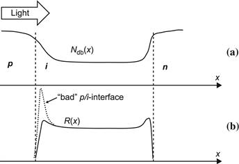
FIGURE 16 Schematic representation of (a) the dangling bond density Edb(x) and (b) the recombination function R(x) in the i layer of a p–i–n-type thin-film solar cell; if the cell has a problematic p–i interface (e.g., due to boron contamination from the p layer deposited before the i layer), there will be strong supplementary recombination, as indicated by the dotted line.
(Reproduced from [1] with permission of the EPFL Press.)
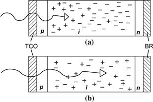
FIGURE 17 Light penetration and presence of photogenerated carriers (holes and electrons) within a p–i–n-type solar cell. (a) For blue, short-wavelength light, recombination only takes place near the p–i interface; (b) for red, long-wavelength light, recombination can take place throughout the i layer. TCO=transparent conductive oxide; BR=back reflector.
(Reproduced from [1] with permission of the EPFL Press.)
For amorphous silicon solar cells, the dangling bond density will be dramatically increased by light-induced degradation (the Staebler–Wronski effect). By keeping the solar cell very thin, i.e., by choosing an i-layer thickness di in the range of 200 to 300 nm, and by adopting all the other measures described earlier (see Section 2.1) one is able today to fabricate amorphous silicon solar cells with a relative efficiency loss of just 10% to 20% due to light-induced degradation.
If the recombination in a thin-film silicon solar cell becomes excessive, the resulting deficiency in photocarrier collection can be mainly identified by: (a) decrease in the fill factor FF; (b) a deficiency in the spectral-response/external quantum efficiency (EQE) curve of the cell. In case (b) it is particularly instructive to compare two EQE-curves: a first curve with no bias voltage and a second curve with a reverse bias voltage of −1 to −2 Volts. If these curves essentially do not differ, the internal electric field at no bias is sufficiently high to collect practically all photogenerated carriers. However, a difference between the two curves (see Figure 18) indicates collection problems, i.e. the internal field must be increased by an external bias to enhance the carrier collection. If the difference is seen at short wavelengths, it means that the collection problem occurs at the interface through which light enters in to the cell (at the p–i interface, for p–i–n-cells illuminated from the p side); if it occurs at longer wavelengths, it means that the collection problem occurs in the bulk of the i layer. Figure 17 represents the difference between (a) blue light and (b) red light entering into a p–i–n-type solar cell. In the case of blue light, there are photogenerated holes and electrons only near the p–i-interface, so that recombination can only take place there. We are, thus, only probing the region of the i layer near the p–i-interface. In the case of red light, holes and electrons are generated throughout the i layer and we are probing the whole i layer.
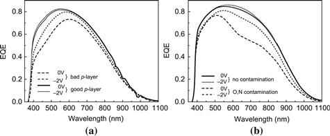
FIGURE 18 External quantum efficiency (EQE) curves of microcrystalline silicon solar cells with various deficiencies (see text).
(Reproduced from [1] with permission of the EPFL Press.)
Figure 18 shows typical external quantum efficiency curves of microcrystalline p–i–n-type cells. In (a) we are looking at cells with different p layers (in the case of the “bad” p layer, it would appear that the recombination in the adjoining regions of the i layer is also increased, possible through cross-contamination or another effect). In (b) we are looking at cells with and without contamination; the contamination results in a reduction or deformation of the electric field and a collection problem throughout the i layer as described earlier.
Spectral-response and EQE measurements are a powerful tool for the diagnosis of thin-film silicon solar cells. Their detailed interpretation needs, however, considerable experience, and goes well beyond the scope of the present chapter. Their main advantage is that they allow us to assign defects and shortcomings to various regions of the cell. Their “geometrical sensitivity” is excellent for the zone where the light enters into the solar cell, but it is very much reduced at the far end of the solar cell toward the back reflector (BR) in Figure 17. In order to probe the far end of the cell, it is necessary to employ a bifacial configuration, in which one can let the light enter “from the back”—i.e., through the n layer—and perform EQE measurements in this arrangement [75].
4.3 Shunts
In thin-film silicon solar cells and modules, shunts are a common problem. Shunts result in a reduction of the fill factor FF already at standard illumination levels of 100 mW/cm2 light intensity. In order to distinguish them from collection problems (which also result in a reduction of the fill factor FF at standard light levels), it is necessary to measure the J-V curve of the cell or module at low light levels. If there is a substantial further drop in the FF as the light level is decreased to less than 1 mW/cm2, we are facing a shunt problem, not a collection problem.
To conceptually separate the effects of collection problems and shunts, look at Figures 19 and 20. Figure 19 shows the common equivalent circuit universally used for all solar cells. This equivalent circuit is indeed very simple and therefore convenient for the design of entire electrical systems containing solar cells and modules. However, it does not provide us with physical insight into what is happening within the solar cell, especially within a thin-film silicon solar cell. In fact, the effects of shunts and of collection problems are merged together in the parallel resistance Rp. In Figure 20. a modified equivalent circuit, introduced by [76] is given: here the recombination or collection problems are symbolized by a “current sink” Jrec (opposite of a current source). The recombination current Jrec is proportional to the photogenerated current Jph and will therefore result in performance reduction and in a FF reduction that is independent of light intensity. The resistance Rshunt represents now “true” Ohmic shunts. From the electrical diagram of Figure 20, one can see that Rshunt will play an increasing role as the light level, and thus, both the photogenerated current Jph and the recombination current Jrec are decreased proportionally to the light level. On the other hand, the current through Rshunt (approximately V/Rshunt) is not reduced to the same extent, because the J-V curves at low light levels show only minimal voltage decreases compared to the current decreases.
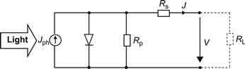
FIGURE 19 Common equivalent circuit universally used for all solar cells. Note that the parallel resistance Rp symbolizes both recombination–collection problems as well as the effect of shunts. RL represents an external load. This simple equivalent circuit is used for designing electrical systems containing solar cells and modules.
(Reproduced from [1] with permission of the EPFL Press.)
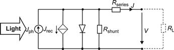
FIGURE 20 Modified equivalent circuit introduced by [76] in order to separate the effects of recombination–collection problems and shunts in p–i–n- and n–i–p-type thin-film silicon solar cells. The current sink Jrec represents current losses through recombination; the value of Jrec is proportional to the value of Jph and depends additionally on the operating point (V) and on the “quality” of the cell; the resistor Rshunt represents “true” Ohmic shunts. This modified equivalent circuit is only used for the analysis of solar cells and modules with unsatisfactory performance.
(Reproduced from [1] with permission of the EPFL Press.)
Shunts in thin-film silicon solar cells can originate from various fabrication problems.
1. Particles may be deposited on the substrates or on the growing layers because of either a dusty environment or the formation of powder during the deposition itself (due to plasma polymerization—i.e., chemical reactions in the gas phase); after the particle falls off, a pinhole remains and a short-circuit will be formed when the final contact layer is deposited (Figure 21) and makes contact to the conducting substrate through the pinhole.
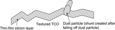
FIGURE 21 Schematic representation of shunt formation due to a dust particle.
(Reproduced from [1] with permission of the EPFL Press.)
2. Mechanical operations (such as cutting of modules) may give rise to the generation of particles.
3. Laser scribing (see Section 6.3) with parameters that are not properly optimized may create partial short circuits within a module, either at locations along a scribe line or by local bridges across a scribe line.
4. Cracks may develop during the growth of the microcrystalline silicon layer (Figure 22) when a rough substrate is used and precautionary measures are not taken [45,77,78].
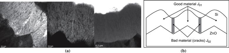
FIGURE 22 (a) Electron micrograph showing the formation of cracks when microcrystalline silicon layers are grown on certain rough substrates (here on a ZnO transparent contact layer) without adequate substrate surface treatment; (b) schematic drawing indicating that these cracks may not only create shunts but also “bad” diodes (diodes with high reverse saturation current J02>J01 due to porous material).
Shunts and collection problems can be quantified with the help of the variable intensity measurement (VIM) method. VIM analysis is based on measuring the J-V characteristics of the solar cell or module for a whole range of light intensities. An evaluation of these curves as indicated in [79,80] will enable us to determine to what extent the performance of the cell or module—and, in particular, its fill factor—are affected by shunts and to what extent they are affected by collection problems.
4.4 Series Resistance Problems
In thin-film silicon solar cells and modules, the electrical contacts are made to the front and back contact layers. Generally the contact on the “front side” (where the light enters into the cell or module) is given by a transparent conductive oxide layer. Here a compromise between optical and electrical requirements must be found: if the TCO layer is chosen to be too thin to keep the optical absorption low, it will have a high sheet resistance and will contribute in a pronounced manner to the series resistance Rseries shown in Figure 20. If the TCO layer is too thick, it will absorb too much light, which is lost for photocarrier generation. The thickness of the back contact layer is less critical, since these layers are either highly conducting metal layers or, in case of TCO layers with additional reflector layers, can be chosen thicker for lower sheet resistance. For small individual laboratory test cells, sheet resistances usually do not cause significant electrical losses.
However, for modules that feature a monolithic series connection of cells (see Section 6.3, especially Figure 33), the earlier mentioned compromise between optical and electrical losses must be carefully taken into account.
For a cell with a photoactive width w, the relative power loss at the maximum power point is given by the expression [42]
![]()
where Rsheet denotes the sheet resistance of the TCO layer and jmp and Vmp are current density and voltage at the maximum power point, respectively. The term (ΔP/P)mp×100% then gives us the reduction in fill factor due to the sheet resistance of the TCO. One can draw the following conclusions from the preceding expression:
1. It is important to use TCO layers with low sheet resistance (typically Rsheet=10Ω/square or lower).
2. The width w of the cell has to be kept very low (in single-junction amorphous silicon solar cells, the widths of individual cells within a solar panel are kept typically below 1 cm). However, the cell-interconnection scheme implies an area loss, since the required laser scribes to establish the interconnection represent photoinactive area losses (see Section 6.3). For a certain interconnection width Δw, the relative area loss is Δw/(w+Δw), where w is the photoactive cell width—i.e., the area loss increases, opposite to the electrical loss, with decreasing cell width. Thus, there is an optimal width in which the sum of electrical and area losses reaches a minimum.
3. For cells with high current and low voltage (like single-junction microcrystalline silicon solar cells), the relative power loss will be higher; this is one reason why we do not fabricate modules with single-junction microcrystalline cells).
4. For tandem cells, and even more for triple-junction cells, the relative power loss will be lower, since the inherent series connection of the subcells results in the addition of their voltages and in a lower current corresponding to the shared absorption.
In addition to the sheet resistance of the TCO, poorly doped p and n layers will also contribute to increase the value of Rseries. Furthermore, contact problems between the TCO (which is usually n type) and the adjacent p layer, as well as unsatisfactory tunnel or recombination junctions within tandems and multijunction cells (see Section 5.1) will also lead to an increase in Rseries. If the cell or module is properly designed and fabricated, the loss in fill factor FF due to series resistance Rseries, should, at standard illumination conditions, not exceed a few percentage points. If FF increases when reducing the light intensity, this is typically a sign of losses due to series resistance Rseries. If these losses are excessive, they can be evaluated by VIM analysis [79,80].
4.5 Light Trapping
In thin-film silicon solar cells and modules, it is imperative to limit the thickness di of the i layer (which is usually the only layer contributing to useful absorption and photogeneration) in order to keep the internal electric field sufficiently high for effective carrier collection. A higher value of di, such that the solar cell could absorb a large part of the solar spectrum, would lead to a very high light-induced degradation in amorphous silicon solar cells; in microcrystalline silicon solar cells, it would mean long deposition times and high material and fabrication costs. This can be seen in Figure 23, where the absorption coefficient α and the penetration depth dpen = 1/α of monochromatic light are plotted as a function of the wavelength λ (or of the photon energy Ephoton = hν) of the light. Figure 23 (from [81]) compares five materials commonly used for solar cells. It can be seen that for both CuInSe2 and CdTe the penetration depth dpen is approximately 1 μm or lower for most of the light in the visible range of the solar spectrum—i.e., for light with wavelengths ![]() <700 nm. For the various forms of silicon, this is clearly not the case: dpen is larger than 1 μm for
<700 nm. For the various forms of silicon, this is clearly not the case: dpen is larger than 1 μm for ![]() = 700 nm, and it remains still higher than the corresponding penetration depths for CuInSe2 and CdTe down to wavelengths
= 700 nm, and it remains still higher than the corresponding penetration depths for CuInSe2 and CdTe down to wavelengths ![]() >500 nm.
>500 nm.

FIGURE 23 Absorption coefficient α and penetration depth dpen in function of wavelength λ (top scale) or photon energy Ephoton = hν (bottom scale), for materials commonly used in solar cells: hydrogenated amorphous silicon (a-Si), hydrogenated microcrystalline silicon (with 50% to 60% Raman crystallinity; μc-Si), wafer-based crystalline silicon (c-Si), CdTe, and CuInSe2. Because of the amorphous phase contained in the microcrystalline silicon layers, the curve for μc-Si lies in between the curve for a-Si and c-Si.
In order to absorb a sufficient portion of the incoming light in a thin-film silicon solar cell, it is necessary to increase the average optical path length within the i layer by a factor m. With the help of a back reflector, one may double the optical path and reach m = 2. By using improved light-scattering techniques. one presently reaches substantially higher values of m—around 10 or even higher.
In p–i–n solar cells, this is currently done by using randomly textured TCO layers. Since the texture of the front TCO layer is widely replicated for the back reflector layer, scattering in reflection further increases the optical path length, particularly for the weaker absorbed wavelengths toward the red portion of the incident light.
In n–i–p solar cells, one deposits first the back reflector. By depositing a randomly textured back reflector, such as a rough silver layer [82–84], one obtains light scattering at this point, and, to some extent, also at the entry point of the light—as the layers deposited on top of the back reflector take on more or less the same form.
All present solar cells and modules use randomly textured structures for light scattering; however, from a research point of view, periodical structures for light scattering are increasingly being investigated [85–87].
The design of light-management and light-trapping schemes and their incorporation into thin-film silicon solar cells is by no means trivial. There are a whole series of questions yet to be solved:
1. Which is the best surface–interface structure (morphology) to obtain an extension of the optical path by the greatest possible factor m?
2. Given that there are multiple reflections and multiple points of scattering within a thin-film silicon solar cell, as shown in Figure 24, what is the practical limit for m?
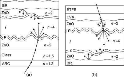
FIGURE 24 Principle of light trapping in (a) p–i–n-type solar cell; (b) n–i–p-type solar cell. The figure shows the case of a single-junction solar cell, with ZnO (zinc oxide) as TCO layer, a back reflector (BR). One notes the multiple interfaces at which scattering and reflection take place. For p–i–n-based modules (a), the front glass is sometimes provided with an antireflective coating (ARC), the encapsulation of the back side, usually done with EVA, is not shown. For n–i–p-based modules (b), ETFE and EVA are typical polymer foils used for encapsulation and needed for protection.
(Reproduced from [1] with permission of the EPFL Press.)
3. How does one avoid cracks and other problems within the silicon layers when choosing a very pronounced texture? (See Figure 22.)
4. Each time that light passes through a doped layer or a TCO layer, and each time light is reflected at a metal reflector (especially at a textured metal reflector), there are losses through optical absorption. How do we minimize them? (This question is particularly important for μc-Si:H solar cells, which absorb the light in the near infrared, where there are additional optical losses through free-carrier absorption—e.g., see [88].)
It can therefore be stated that improved light management and light trapping techniques hold great promise for further enhancing the performance of thin-film silicon solar cells.
5 Tandem and Multijunction Solar Cells
5.1 General Principles
In thin-film silicon solar cells, one so far almost exclusively uses two-terminal tandem solar cells. These devices stack two subcells, one on top of the other as indicated in Figure 25.
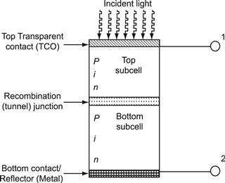
FIGURE 25 Principle of dual-junction stacked cell or tandem cell in the p–i–n configuration, with two electrical terminals; the light is first absorbed in the top subcell; the remaining light enters into the bottom subcell. Electrically, the two subcells are in series, so that strictly the same current circulates through each of them.
In the ideal case, each of the subcells absorbs the same amount of photons and therefore basically photogenerates the same electrical current. This is the case of “current matching,” and it can only be achieved for a given spectrum of the incoming light. If the spectrum of the incident light changes, or if one of the two subcells changes its properties in a more pronounced way than the other (e.g., because of light-induced degradation or because of a difference in temperature coefficients), we will have a mismatch in the two currents; in this case, the subcell with the lower current will limit the current of the tandem. The voltage of the tandem is equal to the sum of the voltages of the two subcells.
As for the fill factor of a tandem, it is difficult to predict. In the case of current mismatch, the fill factor is artificially increased—but because of the loss in current, this does not result in a net increase of the conversion efficiency. One should therefore be very careful when trying to draw conclusions from the value of the fill factor in a tandem (or, even more so, in a multijunction cell) [89].
Why does one designate the intermediate zone between top subcell and bottom subcell as recombination junction or tunnel junction? The electrons photogenerated in the i layer of the top subcell will travel toward the n layer and then enter into the intermediate zone; similarly, the holes generated in the i layer of the bottom subcell will travel toward the p layer and then enter into the intermediate zone. To ensure current continuity, all electrons travelling downward (in Figure 25) will have to recombine with the holes travelling upward. This recombination process is in general facilitated by “tunnelling” of the electrons and holes from the conduction and valence band, respectively, of the doped layers, into imperfection states (midgap defects) localized at the interface (see Figure 26) so that one also uses the term tunnel junction.

FIGURE 26 Principle of tunnel–recombination junction in a tandem cell. All electrons exiting from the top subcell have to recombine with the holes exiting from the bottom subcell; their recombination will be assisted by midgap defects (dangling bonds) situated within this junction and by tunnelling of carriers to the midgap defects.
(Reproduced from [1] with permission of the EPFL Press.)
The tunnel or recombination junction is composed of an n layer and a p layer; at least one of these layers (or, alternatively, the interface between these two layers) should contain a high density of midgap defects to facilitate recombination. Both layers are generally strongly doped, and, if possible, microcrystalline and not amorphous to enable tunnelling. Poorly designed tunnel or recombination junctions will contribute to increase the series resistance of the cell.
What are the advantages of using the tandem configuration instead of the single-junction configuration? There are some evident advantages.
• Currents take on roughly half the value, and voltages double the value, so that the electrical losses due to the TCO sheet resistance are reduced by roughly a factor of 4.
• The i-layer thicknesses of the subcells can be decreased, and hence the internal fields increased, while both thicknesses combined represent a similar absorption length as in a single-junction configuration; thus, in amorphous silicon subcells, the effect of light-induced degradation will be reduced.
• The subcells can have different band gaps and, thus, may cover each a different range of the solar spectrum.
On the other hand, there is the delicate problem of current matching and a significant increase in the complexity of the fabrication process.
5.2 a-Si:H/a-Si:H Tandems
The simplest form of tandem cell is the one shown in Figure 27: an amorphous silicon top subcell is sitting on top of a bottom subcell, which consists also of amorphous silicon. If the band gaps of both subcells were exactly the same, then the i-layer thickness d1 of the top subcell would have to be very much smaller than the i-layer thickness d2 of the bottom subcell; this follows from the exponential absorption profile of the incident light and might lead to either an exceedingly low value of d1 (and thus an increased tendency for the top subcell to have shunts) or a very large value of d2 (with a corresponding undesired light-induced degradation effect in the bottom subcell). Thus, one attempts to increase the band gap of the top subcell—either by alloying with some carbon—i.e., using an a-Si,C:H layer [90]—or by changing the deposition conditions—i.e., by increasing the hydrogen dilution in the deposition plasma) and to decrease the band gap of the bottom subcell (either by alloying with some germanium—i.e., using an a-Si,Ge:H layer—or by changing the deposition conditions—i.e., by decreasing the hydrogen dilution and increasing slightly the deposition temperature). At present, the most successful a-Si:H/a-Si:H tandems do not use any alloying [20]; they can attain a total area stabilized efficiency of more than 7%.
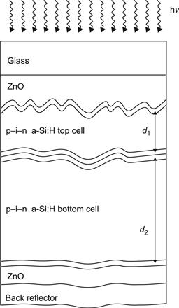
FIGURE 27 Sketch of a fully amorphous tandem cell (here an a-Si:H/a-Si:H tandem).
(Reproduced from [1] with permission of the EPFL Press.)
5.3 Triple-Junction Amorphous Cells with Silicon–Germanium Alloys
Triple-junction cells with amorphous silicon–germanium alloys and modules based on this triple-junction design have been produced since the mid-1990s by the firm United Solar Ovonic. These devices are deposited on stainless steel substrates in an n–i-p sequence (see Figure 28). The light enters into the solar cell through the topmost p layer on which an indium tin oxide layer has been deposited as a TCO. In order to improve (reduce) the contact resistance and correspondingly reduce also Rseries, a metal grid is deposited on top of the ITO layer. The grid has, however, the disadvantage of “shading” the solar cell, thus reducing the photoactive area by almost 10%. In the laboratory, an active-area initial efficiency of 14.6% and an active-area stabilized efficiency of 13% were achieved for small-area cells [21]. The stabilized total-area efficiency is thereby (because of the presence of the grid) only 12.1%: this is at present roughly the same value as the stabilized total-area efficiency of the best micromorph tandem cells (see Section 5.4).
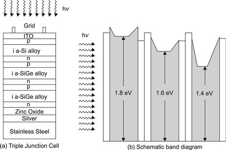
FIGURE 28 Principle of triple-junction cell with an amorphous silicon top subcell and middle and bottom subcells employing amorphous silicon–germanium alloys: (a) basic structure; (b) schematic band diagram showing the variation in band gap within the individual subcells as used in these cells in order to improve carrier collection.
(Reproduced from [1] with permission of the EPFL Press.)
The stainless steel substrates are flexible and thus lend themselves to roll-to-roll fabrication of lightweight, unbreakable modules especially suited for building-integrated photovoltaics. Module efficiencies are, however, considerably lower than the previously mentioned cell efficiencies—about the same value as for tandem a-Si:H/a-Si:H modules on glass. The relatively large discrepancy between the cell and module efficiencies are mainly caused by the method of interconnecting cells to a module (see also Sections 6.2 and 6.3). Unlike the monolithic interconnection that is applicable to nonconducting substrates like glass, relatively large-area cells on the conducting stainless steel substrate are individually connected, very much like the stringing of crystalline silicon cells. These large areas result in large total currents and hence require special precautions to reach low series resistances Rseries. Therefore, the grid mentioned previously is absolutely necessary to balance losses by series resistance with active-area losses. In addition, the deposition rate has to be increased for economic reasons, whereby the layer quality will generally suffer, resulting in lower cell performance.
5.4 Microcrystalline–Amorphous or “Micromorph” Tandems
One of the most promising tandem cells, is the so-called micromorph tandem, containing, as shown in Figure 29, a microcrystalline silicon bottom subcell and an amorphous silicon top subcell. This structure was introduced by the Neuchâtel group in 1994 [91]. It has since then been the focus of intensive R&D efforts and stabilized small-area cell efficiencies of 12% were reported a few years back [92]. The micromorph tandem is of special interest, because the band gap combination of 1.1 eV/1.75 eV, as approximately given by μc-Si:H and a-Si:H, would correspond to the “ideal” band-gap combination for a tandem cell, provided (1) that collection problems can be neglected and (2) that all the photons with energies above the band-gap energy are usefully absorbed in the corresponding subcell [22]. These conditions are, in practice, far from being fulfilled. The amorphous top subcell suffers from the light-induced degradation effect (Staebler–Wronski effect) and therefore has to be kept as thin as possible, with an i-layer thickness di of 200 nm (or less). This means that the top subcell will not absorb enough light.

FIGURE 29 Microcrystalline–amorphous or micromorph tandem cell: (a) basic structure (note that the intermediate reflector between the two subcells is not drawn); (b) electron micrograph.
(Reproduced from [1] with permission of the EPFL Press.)
The remedy used here to enhance photogeneration in the amorphous top subcell is to provide an intermediate reflector (IR) between the top and the bottom subcells in such a way that the short-wavelength components of the light are reflected back into the amorphous top subcell but the long-wavelength components are (as far as possible) passed on, with little attenuation, into the microcrystalline bottom subcell. As intermediate reflector, one needs basically a material with a refractive index n lower than that of amorphous or microcrystalline silicon (n≈4). Physically, a ZnO layer, with a refractive index n = 2, is an excellent candidate; it was used in the first trials [93]. But ZnO is not a very convenient solution from the fabrication point of view, so later solutions, including doped silicon oxide layers, were introduced. These layers can be conveniently deposited by plasma deposition, just like the a-Si:H and μc-Si:H layers themselves (see [94–96]). The design of an efficient and spectrally selective intermediate reflector remains one of the primary research topics for micromorph tandems [97].
The microcrystalline bottom subcell has also to be kept as thin as possible. Here it is not the light-induced degradation, but the fabrication cost, that is the issue, The fabrication costs associated with the deposition of the microcrystalline silicon intrinsic layer are one of the main cost factors for micromorph module production. On one hand, the plasma-deposition equipment represents a very large investment. Now operation and depreciation costs for the plasma reactor are proportional to layer thickness. If the layer, which has to be deposited, is thick, the deposition process will correspondingly take a long time, thus diminishing the production throughput. Furthermore, the materials costs for gas inputs into the plasma reactor (silane and hydrogen) are also proportional to the thickness of the deposited layer. Therefore, one currently proposes to use microcrystalline silicon bottom cells with a total thickness of less than 1 μm [23]. Referring to Section 4.5, and particularly to Figure 23, one can immediately see that this will only be possible with a very effective light-trapping scheme. The multiplication factor m by which the optical path becomes longer than the intrinsic layer thickness di should be as high as 10, or even higher, in order to absorb a sufficiently large part of the incoming light.
Thus, one may state that most of the research problems to be solved in the coming years, in order to increase the efficiency of micromorph tandems, are related to improvements in light management (e.g., see [98]).
An interesting further development of the micromorph tandem concept is the extension to triple-junction cells. In these triple-junction cells, one generally retains an amorphous subcell on top and a microcrystalline subcell on the bottom. For the middle subcell, however, a number of different possibilities have been tried out.
• An amorphous silicon–germanium alloy (a-Si,Ge:H): the disadvantages are here (1) the relatively high cost of germanium and (2) the pronounced light-induced degradation present in these alloys.
• A microcrystalline silicon (μc-Si:H): the disadvantages here are (1) the low open-circuit voltage Voc that can be achieved with such a subcell, (2) light-management problems (i.e., how to obtain a high enough current with a sufficiently thin μc-Si:H middle subcell?), and (3) higher fabrication costs associated with the deposition of two microcrystalline subcells.
• Unalloyed amorphous silicon (a-Si:H): the disadvantages here are linked to light-management problems and to the light-induced degradation effect.
One comes therefore to the conclusion that today there does not exist so far a clear preference for the structure of micromorph triple-junction cells. The different possibilities need further in-depth investigation, especially with respect to the light-management problem, which now truly becomes quite complex. On the other hand, if one goes for the triple-junction configuration and the increased fabrication costs associated with such a configuration, then one would hope to be able to avoid the use of intermediate reflectors.
6 Module Production and Performance
6.1 Deposition of the Thin-Film Silicon Layers
The deposition of the thin-film silicon layers is the central step in the fabrication of solar modules based on amorphous and microcrystalline silicon. The method generally used—by all manufacturers up to now is plasma-enhanced chemical vapour deposition (PECVD) in a capacitively coupled reactor, as indicated schematically in Figure 30. For the deposition of the intrinsic layers, a mixture of silane and hydrogen is used; for the deposition of the relatively thin doped layers, diborane or trimethlyboron is added for the p layer, and phosphine is added for the n layer (see Section 2.3).
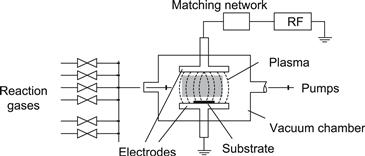
FIGURE 30 Capacitively-coupled plasma-deposition system.
(Reproduced from [1] with permission of the EPFL Press.)
At present, the deposition of the intrinsic silicon layer is the production step that takes the largest share of total module production costs. It is also one of the most critical steps from the point of view of module performance. The high production costs for this fabrication step stem principally from two factors:
1. High investment costs necessary for the PECVD equipment. This means that depreciation and operating costs are correspondingly high. In order to reduce this part of module fabrication costs, one strives to keep the total deposition time for the intrinsic layers as low as possible by
a. making the intrinsic layers as thin as possible (this is a question of light management—see Section 4.5) and
b. increasing the deposition rate for the intrinsic layer without reducing layer quality; this aspect will be treated hereunder.
2. Consumption of process gases, especially of silane and hydrogen. To minimize this part of fabrication costs, one has to
a. keep the intrinsic layers as thin as possible, as just mentioned;
b. use a plasma-deposition process in which a large part of the silicon contained in the silane gas fed into the deposition system is actually deposited as thin-film layer; and
c. use process parameters that allow for layer deposition with only a moderate hydrogen dilution ratio (this last criterion is specially critical for the deposition of microcrystalline silicon layers).
A capacitively coupled plasma-deposition system, as indicated in Figure 30, contains electrically neutral molecules, some of which are the growth radicals, actively contributing to layer growth. It also contains electrons and positively charged ions. Increasing the deposition rate is generally accomplished by increasing the electrical power fed into the deposition system. This not only increases the densities of growth radicals but also enhances the ion bombardment on the growing silicon layer. High-energy ion bombardment generally leads to the creation of additional defects on the growing layer and must therefore be avoided. The following are the two most common methods to avoid high-energy ion bombardment.
1. Increase the plasma excitation frequency from the standard industrial frequency of 13.56 MHz to frequencies in the very high frequency (VHF) range, typically to frequencies between 60 and 100 MHz [99,100]. As the plasma excitation frequency is increased, the so-called sheaths—i.e., thin regions with strong electrical fields next to each of the electrodes in Figure 30—become thinner. The voltage drop across the sheaths is reduced and, accordingly, the positive ions hitting the growing silicon surface are not accelerated to the same extent [101]. Note, however, that the design of a large-area deposition system becomes more difficult as the plasma excitation frequency is increased and the corresponding wavelength of the electrical field powering the plasma is decreased and approaches the dimensions of the electrode. As a consequence, the deposition tends to become nonuniform [102]. Uniform deposition can then only be achieved with a relatively sophisticated (and costly) design of the deposition system; one uses, e.g., lens-shaped [103] or ladder-shaped [28] electrodes.
2. An increase in the deposition pressure: at higher pressures there are more collisions between the various species in the plasma, reducing thereby the energies of the ions impinging upon the growing surface. To arrive at the highest deposition rates, relatively high pressures are combined with high excitation frequencies [104].
There are a number of other factors that have to be taken into account when designing a deposition system for thin-film silicon layers.
1. The formation of powder during deposition must be avoided. Powder is formed by premature chemical reactions in the gas phase—i.e., by so-called plasma polymerization. An increase in plasma excitation frequency, in general, will lead to reduced powder formation [105].
2. The presence of powder during deposition, on the other hand, will lead to shunts in the solar cell being fabricated. There is therefore a need to periodically clean the deposition system; this is traditionally done by plasma etching with relatively powerful etchant gases such as SF6 and NF3. These gases are, however, “greenhouse gases” [106], which contribute to global warming; their use in industrial systems is therefore increasingly being avoided. Instead, one turns to alternative cleaning gases such as fluorine [107] or reverts to purely mechanical cleaning procedures—the latter are, however, cumbersome and can entail health problems for the workers involved in the process.
3. The need to minimize gas consumption and maximize gas utilisation. This factor needs at present to be investigated in more detail: there is some published work on silane utilisation [108]. On the other hand, an increase in deposition pressure seems to result generally in a strong increase of hydrogen consumption for microcrystalline layers.
4. The need to avoid the deposition of porous layers, which quite generally have inferior quality (they lead to solar cells with higher degradation and ageing effects and, in more extreme cases, to solar cells with lower initial efficiencies).
The design of economically attractive deposition systems for thin-film silicon modules is therefore a very important topic, which will have a decisive effect on the future success of this type of modules.
To conclude, one may remark that hot wire deposition (also called catalytic CVD) is increasingly being proposed and tested as an interesting alternative to plasma deposition (e.g., see [109–112]). This method is, however, at present not yet used in industrial module fabrication. Hot wire deposition completely avoids ion bombardment; instead of a plasma, one uses a filament heated to very high temperatures (around 1800°C) to obtain silane dissociation and generation of growth radicals. This method also has the advantage of a relatively high gas utilisation. Potentially it should be able to lead to the fabrication of solar modules at high deposition rates and with excellent performances. Excellent solar cells have up to now been fabricated by hot wire deposition at low deposition rates, and individual layers with excellent properties have also been fabricated at high deposition rates. But the combination of a high efficiency and a high deposition rate has so far only been demonstrated in isolated cases. Furthermore, it would seem that a certain amount of ion bombardment with low-energy ions may, in some cases, be beneficial for the fabrication of solar cells. Thus, the combination of plasma deposition and hot wire deposition [113] may be especially interesting to investigate.
6.2 Substrate Materials and Transparent Contacts
There are basically two possible configurations for thin-film silicon solar cells.
1. In a so-called superstrate configuration (indicated schematically in Figure 31), where glass is used as the support on which the solar cell is deposited and at the same time also as cover through which light enters into the solar cell. As the glass support is on top of the finished modules (facing the incident light) this is called the superstrate configuration, although one generally continues to use the term substrate for the glass when referring to the fabrication process. In this case, one deposits first those silicon layers through which the light enters into solar cell. Here, the deposition sequence is p–i–n for amorphous silicon solar cells; it is advantageous if the light enters into the cell through the p layer and not through the n layer, as explained in Section 4.1. The main advantages of using glass are (a) subsequent deposition of the solar cell is relatively straightforward, (b) glass offers good protection against environmental influences, and (c) glass is known to remain stable for a very long time when exposed to sunlight and if adequately designed to withstand extreme weather conditions. The disadvantages of using glass are (a) weight, (b) possibility of damage through breaking, and (c) rigidity—a limitation for certain applications.
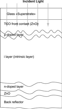
FIGURE 31 Sketch (not drawn to scale) showing basic structure of a single-junction thin-film silicon solar cell in the «superstrate configuration». The thickness of the glass–TCO combination is basically determined by the glass thickness, ranging from 0.5 mm to 4 mm, whereas the TCO layer thickness is typically around 1 μm. The p–i–n layer sequence and back reflector combined amount also to about 1 μm in thickness. The sketch merely illustrates the succession of different layers. Note that the ZnO between the n layer and the back reflector is used only for optical index matching and can therefore be very thin if the back reflector is an electrically conductive and highly reflecting material. If the back reflector is a dielectric layer (e.g., white paint), the adjacent ZnO has to act as a contact layer and be correspondingly thicker, subject to similar requirements as for the front TCO discussed in Section 4.4. To protect against environmental effects, various materials for encapsulation at the back of the cell structure (not shown) are being employed.
2. In the substrate configuration, which is shown schematically in Figure 32, light enters into the cell from the opposite side, and the substrate is the bottom layer. The deposition sequence, in this case, is n–i–p. The substrate does not need to be transparent; the most common substrate used here is stainless steel, a solution pioneered by the firm United Solar Ovonic. Because stainless steel is electrically conducting, it does not lend itself easily to the monolithic cell-interconnection scheme described in the Section 6.3. In fact, the solar cells produced by the firm United Solar Ovonic are connected by separate external wiring to form modules. Deposition of thin-film silicon solar cells on stainless steel has the advantage of being relatively straightforward. Increasingly, one attempts to use polymers as substrates. Here solar cell deposition is more difficult, because it is impaired by outgassing from the polymer and by temperature limitations of the latter. On the other hand, polymers are electrically isolating and can be used together with the monolithic cell-interconnection scheme, which is described later. Many polymers are initially transparent but become yellow under the influence of the UV component within sunlight. They therefore cannot be used in the same manner as glass is used in the superstrate configuration—i.e., as protective cover material. Indeed, in the substrate configuration, a protection layer or cover material must be added to rule out environmental effects. It should come in the form of flexible foil, which has (just like glass) to be transparent, mechanically stable, and UV resistant. This protection foil is one of the important cost factors for the substrate configuration. At present one mainly uses ethylene tetrafluoroethylene (ETFE) as protection foil. The substrate configuration is generally used to fabricate lightweight, flexible, and unbreakable modules that are particularly suited for transport to remote locations and for building-integrated PV (BIPV), particularly for roof integration.
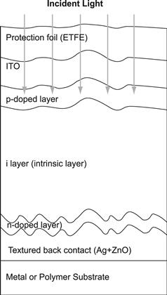
FIGURE 32 Sketch (not drawn to scale) showing basic structure of a single-junction thin-film silicon solar cell in the «substrate configuration». The substrate and the protection foil are each about 0.1 to 0.2 mm thick; the entire cell structure, including the ITO front contact layer and triple-junction structures, are typically about 1 μm thick. The sketch merely illustrates the succession of different layers.
Most manufacturers opt at the moment for the superstrate configuration. Here the glass is coated with a transparent conductive oxide serving as a front contact. For commercial modules, one so far employs mostly fluorine-doped SnO2 as TCO material; SnO2 is usually deposited by atmospheric pressure chemical vapour deposition (APCVD) “online” within the float-zone process employed for glass production [114]. This is probably the most cost-effective way of producing the glass substrate together with the transparent front contact. As mentioned in Section 4.5, the transparent contact has to be textured in order to obtain light trapping. In the case of the present SnO2 layers, which are manufactured online, the texturing is generally not optimized for light trapping in a particular cell configuration. One is therefore currently developing highly textured SnO2 layers with off-line processes on a pilot-line basis (e.g., see [115]). If these experimental processes lead to the desired result, one will probably attempt later to incorporate them (if possible) as an online version within the float-zone process of the glass producer. (Note that SnO2 is chemically reduced by a high-power hydrogen-rich plasma as used for depositing μc-Si:H. Therefore, if one deposits a μc-Si:H solar cell on a SnO2 layer, one has first to cover the latter by a thin protective layer of TiO2 or ZnO. This consideration is of importance for the deposition of single-junction μc-Si:H cells, as studied in research laboratories, but it is irrelevant in case of micromorph tandems, where the SnO2 is no longer exposed to the extreme deposition conditions mentioned previously but is instead protected by the amorphous top subcell, which is deposited first.)
As an alternative to SnO2, one is at present increasingly introducing ZnO as transparent contact material [116]. ZnO acts as an effective diffusion barrier against any contaminants diffusing from the underlying glass substrate. Another advantage is that it can be deposited in a relatively easy manner by the manufacturer of the thin-film solar cell and at a lower deposition temperature than SnO2. There are two main deposition methods for ZnO: (a) sputtering and (b) low-pressure chemical vapour deposition (LPCVD). Sputtering leads to smooth layers that have to be chemically etched in order to obtain the desired texture for light trapping. Sputtered ZnO layers are generally doped with aluminium in order to obtain the desired high conductivity. The LPCVD process leads directly to textured ZnO layers, which have a high effectiveness for light trapping. LPCVD ZnO layers are generally doped with boron.
In the substrate configuration, the TCO front contact layer is deposited at the end of the deposition process. It has correspondingly to be deposited at a relatively low temperature (typically <200°C). Therefore, SnO2 is not an option to be considered. One can use ZnO. One can also use indium tin oxide (ITO=0.9 In2O3/0.1 SnO2). Note that ITO is never used in the superstrate configuration because the In2O3 would be strongly chemically reduced by the exposure to hydrogen during the initial phases of the PECVD, and thus, ITO would widely loose its transparency. Besides, indium would diffuse into the silicon layers, rendering the latter unusable.
Substrates and transparent contact layers, as well as reflecting layers, are an important part of any thin-film silicon cell. They determine to a large extent the performance (especially the current density) of the solar cell. The interaction of textured front and back layers is complex and different for the superstrate and substrate configurations. (See [117] for an analysis, which is restricted, however, to the case of single-junction microcrystalline solar cells.) These front and back layers are therefore increasingly the focus of current research efforts, as already described in Section 4.5. The focus on these parts of the solar cell is all the more warranted, as they also account for a significant part of the total fabrication cost—together with other “external features,” cell-interconnection schemes (see Section 6.3), module encapsulation, and current collection schemes (e.g., metallic grids that can be helpful in reducing the series resistance).
6.3 Laser Scribing and Cell Interconnection
Individual cells have to be electrically interconnected, most often by a series connection in order to form a complete module. Whenever the thin-film silicon solar cell has been deposited on an electrically isolating material, such as glass or polymer, one uses a monolithic interconnection scheme as shown in Figure 33. (The monolithic interconnection scheme cannot be used if the thin-film silicon solar cells have been deposited on an electrically conductive substrate, like stainless steel, unless an isolating interlayer is first deposited. Such an interlayer would, however, be prone to electrical shorts, and would lead to additional complications or costs.)
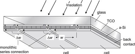
FIGURE 33 Monolithic series connection of thin-film silicon solar cells (photoactive cell width w, photoinactive interconnection width Δw).
(Reproduced from [1] with permission of the EPFL Press.)
In the monolithic interconnection scheme one proceeds as follows if one is using the superstrate configuration with a glass superstrate.
1. The front TCO is deposited on the glass sheet.
2. The front TCO layer is cut into stripes; this separation is best done by removing the TCO with a process called laser scribing [118].
3. The semiconductor layers are deposited in the sequence p–i–n (or p–i–n, p–i–n for tandem cells).
4. These semiconductor layers are now also cut into stripes of the same width as that of the TCO stripes, with scribe lines slightly offset from the previous TCO scribe lines. This separation is again preferably done by laser scribing. Thus, the grooves of the semiconductor layer lie directly above an unremoved area of the front TCO.
5. The metallic (or ZnO) back contact is deposited. This back contact layer thus makes contact with the front TCO layer through the grooves in the semiconductor layer.
6. Finally, the metallic (or ZnO) back contact is “cut up” into stripes of the same width as the previous stripes, once again with a slight offset from the previous semiconductor scribe below. Thus, one arrives at a series-connection structure, where the photoactive cell width is w (taking into account two photoinactive spacings between the three scribes) and the total width of the interconnection is Δw (the cross-section of this structure is shown in Figure 34).
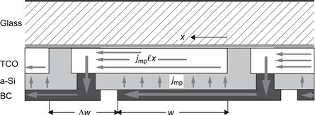
FIGURE 34 Monolithic series connection of thin-film silicon solar cells, shown as cross-section, with corresponding current paths (photoactive cell width w, photoinactive interconnection width Δw, cell length l, current density at the maximum power point jmp, back contact BC).
(Reproduced from [1] with permission of the EPFL Press.)
For optimal cell performance, the photoinactive interconnection width Δw should be as low as possible; it is given by the precision and reproducibility of the laser-scribing system. In the best cases, it is around 0.2 mm [119]. The interconnection area, defined by Δw×l, is lost for photocarrier generation. Thus, there is a relative loss of incoming light, given by (Δw)/(w+Δw).
This loss term (areal loss) decreases with increasing stripe width w. On the other hand, because of the sheet resistance Rsheet of the TCO layer, there is an increase in series resistance Rseries and a corresponding electrical loss of the solar cell leading to a relative power loss, which is proportional to w2, as given in Section 4.5. The sum of the relative areal and electrical losses reaches a minimum for an optimum value of w. This value is of the order of 1 cm, with slightly lower values for single-junction cells and slightly higher values for tandems.
The monolithic series connection can also be applied to the substrate configuration, as long as one is using an isolating substrate such as a polymer sheet. In this case, the laser-scribing process is, for technological reasons, a little more delicate to implement.
If the laser-scribing system is not properly adjusted, partial short circuits will be created on the module; this will lead to low values of shunt resistance Rshunt and to a low fill factor FF. Such a situation is definitely to be avoided.
The monolithic series connection of cells to form large-area modules is one of the key features of thin-film solar cell technologies, ensuring a higher degree of automation and an enhanced reliability, as compared to the stringing procedures used for interconnecting cells in wafer-based crystalline silicon technologies.
6.4 Module Encapsulation
Module encapsulation is indeed a key factor determining the long-term reliability of photovoltaic solar modules. It is an especially critical factor for thin-film modules. For all thin-film modules, one of the main goals of module encapsulation is to protect the semiconductor layers, as well as the transparent contact layers, against the influx of humidity. To this end, special polymer foils and dedicated sealing techniques have been developed. Many different combinations are used in commercial modules; most solutions are proprietary. Thus, at present we can only emphasize the importance of this step. For general information on this problem, the reader is referred to [120–122].
6.5 Module Performance
There are several factors influencing the performance of photovoltaic modules under actual application conditions:
1. spectrum of the incoming light,
2. intensity of the incoming light,
The spectrum of sunlight tends to change over the course of the day (with a shift toward the red in the morning and evening). It also changes with climatic and geographical conditions (with a shift toward the blue in the presence of snow and water surfaces). In general, single-junction amorphous silicon modules perform better than crystalline silicon modules under blue shift of the incoming light and worse than the latter under red shift. Note that a blue shift is regularly observed for indoor conditions, especially for illumination with energy-saving light sources (e.g., fluorescent lamps). As for tandem and multijunction cells, they are more sensitive to changes in the incident spectrum than single-junction cells [123]. This means they must be carefully designed for the average spectrum prevailing in actual field conditions at the site of deployment.
As the intensity of the incoming light is varied from standard conditions (intensity of approximately 100 mW/cm2) to lower values, the conversion efficiency of the cell will be reduced. The extent of this reduction depends very much on the shunt resistance Rshunt within the cell, and this parameter in turn depends on the fabrication process. A low value of Rshunt (and a poor solar cell performance at low light intensities) is an indication of a faulty manufacturing process. Amorphous silicon solar cells with well-mastered fabrication processes can exhibit a very high value of Rshunt and thus also excellent performance for very low light intensities, making them particularly suitable for indoor applications [124]. On the other hand, present thin-film silicon solar cells and modules are not suited for higher light intensities—i.e., for applications with sunlight concentration.
As for the angle of incidence of the incoming light, it evidently also has, for optical reasons, an influence on the efficiency of the solar module. Its influence depends on the module design, especially on the first layers, sheets, or foils through which light enters the solar module. Thus, it is almost impossible to make any general statements. Nevertheless, as the design and the fabrication of solar modules become more standardized and as their application progresses, this effect should be taken into consideration and experimentally quantified (see also [125]).
One of the most important factors that result in reduced solar module efficiency is higher module operating temperature. Figure 35 shows how various solar cell technologies show a decrease in efficiency when their operating temperature is higher than 25°C (the temperature for which the module efficiency is specified in the data sheets—it corresponds to the standard test conditions, STC). One clearly notes from Figure 35 that wafer-based crystalline silicon modules suffer a relative loss in efficiency of about 20% when their operating temperature is increased from 25°C to 75°C (curves a, b, and c in Figure 35), whereas thin-film silicon modules suffer a relative loss of only half that value (curves d and e in Figure 35). In very many applications, the solar modules are typically operating at higher temperatures—between 60°C and 80°C. This is true for applications in tropical countries, and also for BIPV in temperate countries during the summer months. Thus, thin-film silicon solar modules have a “hidden” advantage over wafer-based crystalline silicon modules that does not transpire from the datasheets: their efficiency drop at higher temperatures is much less pronounced (see also [123,126]).
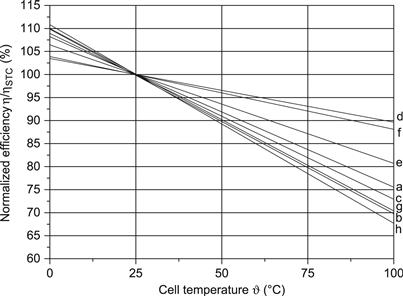
FIGURE 35 Effect of cell operating temperature on cell efficiency, normalized to the efficiency value at standard test conditions (STC)—i.e., to ηSTC (at 25 °C). a, b, c = different types of crystalline wafer-based modules; d = amorphous silicon module; e = micromorph tandem module; f = CdTe module; h, g = CIGS modules.
(Courtesy of Wilhelm Durisch, PSI, Villigen, Switzerland. Reproduced from [1] with permission of the EPFL Press.)
Because of the various effects described previously, the so-called relative performance of photovoltaic installations containing thin-film silicon solar modules is, in general, about 10% higher than that of installations with wafer-based crystalline silicon modules (see [1], Table 6.4). Note that the “relative performance” is given in kWh/kWp and denotes the total amount of electrical energy in kWh delivered by the module during the period of one year, divided by the nominal installed power in kWp.
6.6 Field Experience
The field experience is a very important aspect: only with actual data from modules exposed over several years to outdoor light and weather conditions can we judge whether a given solar technology is mature enough for widespread practical deployment as an energy source.
Amorphous silicon modules have now been in operation for almost 30 years. Whereas modules produced during the 1980s did have unexpected problems and failures, the next generation of modules that came on the market in the 1990s have shown remarkably stable and reliable performance. Chapter 7 in [1] gives several examples of photovoltaic installations, in Europe, in the USA and in Brazil, with performance data for 10 years or more; in all cases, the performance is indeed quite stable after an initial phase of 1 to 2 years with distinct degradation due to the Staebler–Wronski effect (see Section 2.1). In the long run, all photovoltaic modules show some drop in efficiency [127]—i.e., a yearly relative decrease Δη/η in efficiency, of about 0.5%, due partly to the imperfections of the encapsulation. For amorphous silicon modules, Δη/η may be slightly higher, possibly about 1%. Micromorph modules (i.e., modules with microcrystalline–amorphous silicon tandem cells) have not been around for very long so that we do not have long enough field experience with these types of modules; however, from what has so far been observed, one may reasonably expect their long-term performance to be slightly better than that of amorphous silicon modules. A further reason to have full confidence in “micromorph” modules is that the fabrication processes and individual layers used here are very similar (and partly identical) to those used for amorphous silicon modules.
7 Conclusions
Thin-film silicon solar cells and modules have at present a significant disadvantage with respect to wafer-based crystalline silicon modules and even with respect to some other thin-film modules such as CIGS modules: their conversion efficiency is quite a bit lower. Commercial large-area modules do have efficiencies that are now nearing 10% for micromorph tandems. But commercial wafer-based crystalline silicon modules have efficiencies that can lie in the 15% to 18% range. And we may expect efficiencies to slightly increase over the coming years for all technological options. Thus, the relative disadvantage of thin-film silicon modules regarding efficiencies cannot be expected to disappear in the future (although it is somewhat mitigated by the better annual relative performance in kWh/kWp, see Section 6.5).
However thin-film silicon modules also have significant advantages, which may become decisive in the coming years:
1. Only abundant and nontoxic raw materials are used (they share this advantage, of course, with wafer-based crystalline silicon modules).
2. If properly designed, their fabrication process is nonpolluting (just like the fabrication process for wafer-based crystalline silicon modules).
3. The temperature dependence of the PV performance is significantly lower than for wafer-based silicon modules.
4. The energy required for their fabrication is very low and can be recuperated in less than a year (they share a low energy recovery time with most other thin-film solar technologies; for wafer-based silicon technologies, the energy recovery times are about twice that of thin-film technologies).
5. The temperatures used in the fabrication process for thin-film silicon modules are around 200°C and thus much lower than those used for most other solar technologies. This advantage is of special significance for the deposition of thin solar cells on lightweight polymer substrates.
6. Large-area modules can be easily fabricated on substrates exceeding 1 m2 area, with monolithic interconnection of the individual cells.
For all these reasons we can expect thin-film silicon to remain an interesting option for solar cells and modules in the coming decades. Research and development efforts for thin-film silicon modules are continuing worldwide and with high intensity; one may, thus, expect that significant progress will still be achieved for both efficiency and cost.
The future cost and deployment of various solar technologies depends on factors that cannot be exactly foreseen, like the cost and availability of various raw materials—and that of electricity as needed for large-scale module production, especially for crystalline silicon wafers. However, the unique combination of properties 1 to 6 listed previously is so far not matched by any other solar technology. This probably means that thin-film silicon will remain the most interesting option for at least a part of solar applications in the foreseeable future.
References
1. Shah A, ed. Thin-Film Silicon Solar Cells. EPFL Press 2010;.
2. Chittick RC, Alexander JH, Sterling HF. Preparation and properties of amorphous silicon. J Electrochem Soc. 1969;116:77–81.
3. Spear WE, Le Comber PG. Substitutional doping of amorphous silicon. Solid State Commun. 1975;17:1193–1196.
4. Spear WE, Le Comber PG. Electronic properties of substitutionally doped amorphous Si and Ge. Phil Mag B. 1976;33:935–949.
5. Carlson DE, Wronski CR. Amorphous silicon solar cells. Appl Phys Lett. 1976;28:671–673.
6. Carlson DE, Wronski CR, Triano A, Daniel RE. Solar cells using Schottky barriers on amorphous silicon. Baton Rouge: Proceedings of the 22nd IEEE Photovoltaic Specialists Conference; 1976; 893–895.
7. Staebler DL, Wronski CR. Reversible conductivity change in discharge produced amorphous silicon. Appl Phys Lett. 1977;31:292–294.
8. Benagli S, Borrello D, Vallat-Sauvain E, et al. High- efficiency amorphous silicon devices on LPCVD–ZnO TCO prepared in industrial KAI TM-M R&D reactor. Proceedings of the 24th EC PV Solar Energy Conference 2009; pp. 2293–2298.
9. Veprek S, Marecek V. The preparation of thin layers of Ge and Si by chemical hydrogen plasma transport. Solid State Electron. 1968;11:683–684.
10. Usui S, Kikuchi M. Properties of heavily doped glow-discharge silicon with low resistivity. J Non-Crystalline Solids. 1979;34:1–11.
11. Wang C, Lucovsky G. Intrinsic microcrystalline silicon deposited by remote PECVD: A new thin-film photovoltaic material. In: Proceedings of the 21st IEEE Photovoltaic Specialists Conference. 1990;1614ff. .
12. Faraji M, Gokhale S, Choudari SM, Takwale MG, Ghaisas SV. High mobility hydrogenated and oxygenated silicon as a photo-sensitive material in photovoltaic applications. Appl Phys Lett. 1992;60:3289–3291.
13. Flückiger R, Meier J, Keppner H, et al. Microcrystalline silicon prepared with the very high frequency glow discharge technique for p–i–n solar cell applications. Proceedings of the 11th EC PV Solar Energy Conference 1992; pp. 617ff.
14. Meier J, Flückiger R, Keppner H, Shah A. Complete microcrystalline p–i–n solar cell—Crystalline or amorphous cell behaviour?. Appl Phys Lett. 1994;65:860–862.
15. Meier J, Torres P, Platz R, et al. On the way towards high effciency thin film silicon solar cells by the “micromorph” concept. Proc Mater Res Soc Symp. 1996;420:3–14.
16. Torres P, Meier J, Flückiger R, et al. Device grade microcrystalline silicon owing to reduced oxygen contamination. Appl Phys Lett. 1996;69:1373–1375.
17. Van den Donker MN, Klein S, Rech B, Finger F, Kessels WMM, van de Sanden MCM. Microcrystalline silicon solar cells with an open-circuit voltage above 600mV. Appl Phys Lett. 2007;90 (Paper No. 183504).
18. Yan BJ, Yue GZ, Yan YF, et al. Correlation of hydrogen dilution profiling to material structure and device performance of hydrogenated nanocrystalline silicon solar cells. Proc Mater Res Soc Symp. 2008;1066:61–66.
19. Smirnov V, Reynolds S, Finger F, Carius R, Main C. Metastable effects in silicon thin films: Atmospheric adsorption and light induced degradation. J Non- Crystalline Solids. 2006;352:1075–1078.
20. Lechner P, Frammelsberger W, Psyk W, et al. Status of performance of thin film silicon solar cells and modules. Proceedings of the 23rd EC PV Solar Energy Conference 2008; pp. 2023–2026.
21. Yang J, Banerjee A, Guha S. Triple-junction amorphous silicon alloy solar cell with 14.6% initial and 13.0% stable conversion efficiencies. Appl Phys Lett. 1997;70:2975–2977.
22. Shah A, Vanecek M, Meier J, et al. Basic efficiency limits, recent experimental results and novel light-trapping schemes in a-Si:H, mc-Si:H and “micromorph tandem” solar cells. J Non-Crystalline Solids 2004;338–340 639–645.
23. Knauss H, Salabas EL, Fecioru M, et al. Reduction of cell thickness for industrial micromorph tandem modules. Proceedings of the 25th EC PV Solar Energy Conference 2010; pp. 3064–3067.
24. Matsui T, Chang CW, Takada T, Isomura M, Fujiwara H, Kondo M. Thin film solar cells based on microcrystalline silicon-germanium narrow-gap absorbers. Sol Energy Mater & Sol Cells. 2009;93:1100–1102.
25. Shimizu T. Staebler–Wronski effect in hydrogenated amorphous silicon and related alloy films. Jpn J Appl Phys. 2004;43:3257–3268.
26. Bhattacharya E, Mahan AH. Microstructure and the light-induced metastability in hydrogenated amorphous silicon. Appl Phys Lett. 1988;52:1587–1589.
27. Mahan AH, Williamson DL, Nelson BP, Crandall RS. Characterization of microvoids in device-quality hydrogenated amorphous silicon by small-angle X-ray scattering and infrared measurements. Phys Rev B. 1989;40:12024–12027.
28. Takatsuka H, Noda M, Yonekura Y, Takeuchi Y, Yamauchi Y. Development of high efficiency large-area silicon thin film modules using VHF-PECVD. Sol Energy. 2004;77:951–960.
29. Beyer W, Wagner H, Finger F. Hydrogen evolution from a-Si:C: H and a-Si:Ge:H alloys. J Non-Crystalline Solids. 1985;77–78:857–860.
30. Frammelsberger W, Geyer R, Lechner P, et al. Entwicklung und Optimierung von Prozessen zur Herstellung hocheffizienter grossflächiger Si-Dünnschicht-PV-Module. Abschlussbericht, Bundesministerium für Umwelt, Naturschutz und Reaktorsicherheit 2004; Förderkennzeichen 0329810A.
31. Cohen JD. Electronic structure of a-Si:Ge:H. In: Searle T, ed. Amorphous Silicon and Its Alloys, vol 19 of EMIS Datareviews Series. London: INSPEC; 1998.
32. Finger F, Beyer W. Growth of a-Si:Ge:H alloys by PECVD. In: Searle T, ed. Amorphous Silicon and its Alloys (1998), vol 19 of EMIS Datareview Series. London: INSPEC; 1998.
33. Wickboldt P, Pang D, Paul W, et al. High performance glow discharge a-Si1–xGex:H of large x. J Appl Phys. 1997;81:6252–6267.
34. Yang J, Guha S. Status and future perspective of a-Si:H, a-SiGe:H, and nc-Si:H thin film photovoltaic technology. In: Delahoy AE, Eldada LA, eds. Thin film solar technology. 2009; Proceedings of the SPIE vol. 7409 pp. 74090C1-74090C14.
35. Wronski CR. Review of direct measurements of mobility gaps in a-Si:H using internal photoemission. J Non-Crystalline Solids. 1992;141:16–23.
36. VaneÏcek. M, Stuchlik J, Kocka J, Triska A. Determination of the mobility gap in amorphous silicon from a low temperature photoconductivity measurement. J Non- Crystalline Solids. 1985;77 & 78:299–302.
37. Tauc J, Grigorovici A, Vancu A. Optical properties and electronic structure of amorphous germanium, Physica. Status Solidi. 1966;15:627–637.
38. Mok TM, O’Leary SK. The dependence of the Tauc and Cody optical gaps associated with hydrogenated amorphous silicon on the film thickness: al experimental limitations and the impact of curvature in the Tauc and Cody plots. J Appl Phys. 2007;102 (Paper No.113525).
39. Collins RW, Ferlauto AS, Ferreira GM, et al. Evolution of microstructure and phase in amorphous, protocrystalline and microcrystalline silicon studied by real time spectroscopic ellipsometry. Sol Energy Mater & Sol Cells. 2003;78:143–180.
40. Fontcuberta i Morral A, Roca i Caborrocas P, Clerc C. Structure and hydrogen content of polymorphous silicon thin films studied by spectroscopic ellipsometry and nuclear measurements. Phys Rev B. 2004;69 (Paper No 125307).
41. Street RA. Hydrogenated Amorphous Silicon. Cambridge: Cambridge University Press; 1991.
42. Shah AV, Schade H, VaneÏcek M, et al. Thin-film silicon solar cell technology. Prog Photovolt: Res Appl. 2004;12:113–142.
43. Overhof H, Thomas P. Electronic transport in hydrogenated amorphous semiconductors. Springer Tracts in Modern Physics. vol. 114 Berlin: Springer Verlag; 1989; pp. 26, 77.
44. Python M. Microcrystalline solar cells, growth, and defects, Ph D thesis. University of Neuchâtel 2009; Section 3.8.
45. Python M, Dominé D, Söderström T, Meillaud F, Ballif C. Microcrystalline silicon solar cells: Effect of substrate temperature on cracks and their role in post- oxidation. Prog Photovolt: Res Appl. 2010;18:491–499 (see Section 3.1).
46. Collins RW, Ferlauto AS. Advances in plasma-enhanced chemical vapor deposition of silicon films at low temperatures. Curr Opin Solid St M. 2002;6:425–437.
47. Vallat-Sauvain E, Shah A, Bailat J. Advances in microcrystalline silicon solar cell technologies. In: Poortmans J, Arkhipov V, eds. Thin Film Solar Cells: Fabrication, Characterization, and Applications. Chichester, UK: John Wiley & Sons, Ltd; 2006; In: (http://dx.doi.org/10.1002/0470091282.ch4); 2006.
48. Vallat-Sauvain E, Droz C, Meillaud F, Bailat J, Shah A, Ballif C. Determination of Raman emission cross-section ratio in microcrystalline silicon. J Non-Crystalline Solids. 2006;352:1200–1203.
49. Vanecek M, Poruba A, Remes Z, Beck N, Nesladek M. Optical properties of microcrystalline materials. J Non-Crystalline Solids. 1998;967–972:227–230.
50. Dylla T, Finger F, Schiff EA. Hole drift-mobility measurements in microcrystalline silicon. Appl Phys Lett. 2005;87 (Paper No. 032103).
51. Finger F, Astakhov O, Bronger T, et al. Microcrystalline silicon carbide alloys prepared with HWCVD as highly transparent and conductive window layers for thin film solar cells. Thin Solid Films. 2009;517:3507–3512.
52. Vanecek M, Poruba A, Remes Z, et al. Electron spin resonance and optical characterization of defects in microcrystalline silicon. J Non-Crystalline Solids. 2000;266–269:519–523.
53. Astakhov O, Carius R, Finger F, Petrusenko Y, Borysenko V, Barankov D. Relationship between defect density and charge carrier transport in amorphous and microcrystalline silicon. Phys Rev B. 2009;79 (Paper No 104205).
54. Poruba A, Vanecek M, Meier J, Shah A. Fourier transform infrared spectroscopy in microcrystalline silicon. J Non-Crystalline Solids. 2002;299–302:536–540.
55. Finger F, Carius R, Dylla T, Klein S, Okur S, Günes M. Stability of microcrystalline silicon for thin film solar cell applications. IEE Proc Circ Dev Syst. 2003;150:300–308.
56. Meillaud F, Vallat-Sauvain E, Niquille X, et al. Light-induced degradation of thin-film amorphous and microcrystalline silicon solar cells. Lake Buena Vista, Florida: Proceedings of the 31st IEEE Photovoltaic Specialist Conference; 2005; pp. 1412–1415.
57. Wang Y, Geng X, Stiebig H, Finger F. Stability of microcrystalline silicon solar cells with HWCVD buffer layer. Thin Solid Films. 2008;516:733–735.
58. Meillaud F, Vallat-Sauvain E, Shah A, Ballif C. Kinetics of creation and of thermal annealing of light-induced defects in microcrystalline silicon solar cells. J Appl Phys. 2008;103 (Paper No. 054504).
59. Droz C, Vallat-Sauvain E, Bailat J, et al. Electrical and microstructural characterisation of microcrystalline silicon layers and solar cells. Osaka, Japan: Proceedings of the 3rd World Conference on Photovoltaic Energy Conversion; 2003; pp. 1544–1547.
60. Vetterl O, Gross A, Jana T, et al. Changes in electric and optical properties of intrinsic microcrystalline silicon upon variation of the structural composition. J Non-Crystalline Solids. 2002;299–302:772–777.
61. Matsui T, Kondo M, Matsuda A. Doping properties of boron-doped, microcrystalline silicon from B2H6 and BF3: Material properties and solar cell performance. J Non-Crystalline Solids. 2004;338–340:646–650.
62. Finger F, Mai Y, Klein S, Carius R. High efficiency microcrystalline silicon solar cells with hot-wire CVD buffer layer. Thin Solid Films. 2008;516:728–732.
63. Mai Y, Klein S, Geng X, Hülsbeck M, Carius R, Finger F. Differences in the structure composition of microcrystalline silicon solar cells deposited by HWCVD and PECVD: Influence on open circuit voltage. Thin Solid Films. 2006;501:272–275.
64. Nasuno Y, Kondo M, Matsuda A. Microcrystalline silicon thin-film solar cells prepared at low temperature using PECVD. Sol Energy Mater & Sol Cells. 2002;74:497–503.
65. Nasuno Y, Kondo M, Matsuda A. Passivation of oxygen-related donors in microcrystalline silicon by low temperature deposition. Appl Phys Lett. 2001;78:2330–2332.
66. Kilper T, Beyer W, Bräuer G, et al. Oxygen and nitrogen impurities in microcrystalline silicon deposited under optimized conditions: Influence on material properties and solar cell performance. J Appl Phys. 2009;105 (Paper No. 074509).
67. Beck N, Wyrsch N. Ch Hof, A Shah, Mobility lifetime product—A tool for correlating a-Si:H film properties and solar cell performances. J Appl Phys. 1996;79:9361–9368.
68. Droz C, Goerlitzer M, Wyrsch N, Shah A. Electronic transport in hydrogenated microcrystalline silicon: similarities with amorphous silicon. J Non-Crystalline Solids. 2000;266:319–324.
69. Shah A, Platz R, Keppner H. Thin film silicon solar cells: A review and selected trends. Sol Energy Mater & Sol Cells. 1995;38:501–520.
70. Rose A. Concepts in Photoconductivity and Allied Problems. New York: Wiley-Interscience, John Wiley and Sons; 1963; (see also, http://en.wikipedia.org/wiki/ Albert_Rose/.).
71. Vetterl O, Lambertz A, Dasgupta A, et al. Thickness dependence of microcrystalline silicon solar cell properties. Sol Energy Mater & Sol Cells. 2001;66:345–351.
72. Kroll U, Bucher C, Benagli S, et al. High-efficiency p–i–n a-Si:H solar cells with low boron cross-contamination prepared in a large-area single-chamber PECVD reactor. Thin Solid Films 451–452 2004;525–530.
73. Stückelberger M-E, Shah AV, Krc J, Sculati-Meillaud F, Ballif C, Depseisse M. Internal electric field and fill factor of amorphous silicon solar cells. 20– 25 Honolulu, Hawaii: Proceedings of the 35th IEEE Photovoltaic Specialists Conference (PVSC); June 2010; pp. 1569–1574 (Manuscript No. 360).
74. Hubin J, Shah A, Sauvain E. Effects of dangling bonds on the recombination function in amorphous semiconductors. Phil Mag Lett. 1992;66:115–125.
75. Fischer D, Wyrsch N, Fortmann CM, Shah A. Amorphous silicon solar cells with low-level doped i-layers characterised by bifacial measurements. Louisville: Proceedings of the 23rd IEEE Photovoltaic Specialists Conference; 1993; pp. 878–884.
76. Merten J, Asensi JM, Voz C, Shah AV, Platz R, Andreu J. Improved equivalent circuit and analytical model for amorphous silicon solar cells and modules. IEEE Trans Electron Dev. 1998;45:423–429.
77. Python M, Vallat-Sauvain E, Bailat J, et al. Relation between substrate surface morphology and microcrystalline silicon solar cell performance. J Non-Crystalline Solids. 2008;354:2258–2262.
78. Python M, Madani O, Domine D, Meillaud F, Vallat-Sauvain E, Ballif C. Influence of the substrate geometrical parameters on microcrystalline silicon growth for thin-film solar cells. Sol Energy Mater & Sol Cells. 2009;93:1714–1720.
79. Shah AV, Sculati-Meillaud FC, Berényi ZJ, Kumar R. Diagnostics of thin-film silicon solar cells and solar panels/modules with VIM (variable intensity measurements). Sol Energy Mater & Sol Cells. 2011;95:398–403.
80. Meillaud F, Shah A, Bailat J, et al. Microcrystalline silicon solar cells: Theory and diagnostic tools. Kona Island, Hawaii: Proceedings of the 4th World Conference on Photovoltaic Energy Conversion; 2006; pp. 1572–1575.
81. Shah A, Meier J, Buechel A, et al. Towards very low-cost mass production of thin-film silicon photovoltaic (PV) solar modules on glass. Thin Solid Films. 2006;502:292–299.
82. Banerjee A, Guha S. Study of back reflectors for amorphous silicon alloy solar cell application. J Appl Phys. 1991;69:1030–1035.
83. Banerjee A, Yang J, Hoffman K, Guha S. Characteristics of hydrogenated amorphous silicon alloy cells on a Lambertian back reflector. Appl Phys Lett. 1994;65:472–474.
84. Terrazzoni Daudrix V, Guillet J, Freitas F, et al. Characterisation of rough reflecting substrates incorporated into thin-film silicon solar cells. Prog Photovolt: Res Appl. 2006;14:485–498.
85. Terrazzoni-Daudrix V, Guillet J, Niquille X, et al. Enhanced light trapping in thin-film silicon solar cells deposited on PET and glass. Osaka, Japan: Proceedings of the 3rd World Conference on Photovoltaic Energy Conversion; 2003; pp. 1596–1600.
86. Krc J, Zeman M, Campa A, Smole F, Topic M. Novel approaches of light management in thin-film silicon solar cells. Proc Mater Res Soc Symp. 2007;910:669–680.
87. Ferry VE, Verschuuren MA, Li HBT, et al. Light trapping in ultrathin plasmonic solar cells. Opt Express. 2010;18:A237–245.
88. Faÿ S, Steinhauser J, Oliveira N, Vallat-Sauvain E, Ballif C. Opto-electronic properties of rough LP-CVD ZnO: B for use as TCO in thin-film silicon solar cells. Thin Solid Films. 2007;515:8558–8561.
89. Yan B, Yue G, Yang J, Guha S. Correlation of current mismatch and fill factor in amorphous and nanocrystalline silicon based high efficiency multi-junction solar cells. Proceedings of the 33rd IEEE Photvoltaics Specialists Conference 2008; pp. 1038–1040.
90. Delahoy AE. Recent developments in amorphous silicon photovoltaic research and manufacturing at Chronar corporation. Sol Cells. 1989;27:39–57.
91. Meier J, Dubail S, Flückiger R, Fischer D, Keppner H, Shah A. Intrinsic microcrystalline silicon (mc-Si:H)—A promising new thin film solar cell material. Proceedings of the First World Conference on Photovoltaic Energy Conversion 1994; pp. 409–412.
92. Yamamoto K, Nakajima A, Yoshimi M, et al. A thin-film silicon solar cell and module. Prog Photovolt: Res Appl. 2005;13:489–494.
93. Fischer D, Dubail S, Anna Selvan JA, et al. The “micromorph” solar cell: Extending a-Si:H technology towards thin film crystalline silicon. Proceedings of the 25th IEEE Photovoltaic Specialists Conference 1996; pp. 1053–1056.
94. Yamamoto K, Nakajima A, Yoshimi M, et al. High efficiency thin film silicon hybrid cell and module with newly developed innovative Interlayer. Conf Rec 4th World Conf Photovol Energy Conversion. 2006;2:1489–1492.
95. Buehlmann P, Bailat J, Dominé D, et al. In situ silicon oxide based intermediate reflector for thin-film silicon micromorph solar cells. Appl Phys Lett. 2007;91 (Paper No.143505).
96. Dominé D, Buehlmann P, Bailat J, Billet A, Feltrin A, Ballif C. Optical management in high-efficiency thin-film silicon micromorph solar cells with a silicon oxide based intermediate reflector. Phys. status solidi (Rapid Res Lett.). 2008;2:163–165.
97. Söderström T, Haug F-J, Niquille X, Terrazzoni V, Ballif C. Asymmetric intermediate reflector for tandem micromorph thin film silicon solar cells. Appl Phys Lett. 2009;94 (Paper No. 063501).
98. Bailat J, et al. Recent developments of high-efficiency micromorphs tandem solar cells in KAI-M PECVD reactors. Proceedings of the 25th EC PV Solar Energy Conference 2010; pp. 2720–2723.
99. Curtins H, Wyrsch N, Shah AV. High-rate deposition of hydrogenated amorphous silicon—Effect of plasma excitation-frequency. Electron Lett. 1987;23:228–230.
100. Curtins H, Wyrsch N, Favre M, Shah AV. Influence of plasma excitation frequency for a-Si:H thin film deposition. Plasma Chem. and Plasma Process. 1987;7:267–273.
101. Howling AA, Dorier J-L. Ch Hollenstein, U Kroll, F Finger, Frequency effects in silane plasmas for plasma enhanced chemical vapor deposition. J Vac Sci Technol A. 1992;10:1080–1085.
102. Howling AA, Sansonnens L, Hollenstein C. Electromagnetic sources of non- uniformity in large area capacitive reactors. Thin Solid Films. 2006;515:5059–5064.
103. Sansonnens L, Schmidt H, Howling AA, Hollenstein C, Ellert C, Buechel A. Application of the shaped electrode technique to a large area rectangular capacitively coupled plasma reactor to suppress standing wave non-uniformity. J Vac Sci Technol A. 2006;24:1425–1430.
104. Kondo M, Matsuda A. An approach to device grade amorphous and microcrystalline silicon thin films fabricated at higher deposition rates. Curr Opin Solid St M. 2002;6:445–453.
105. Dorier J-L. Ch Hollenstein, A.A Howling, U Kroll, Powder dynamics in very high frequency silane plasmas. J Vac Sci Technol A. 1992;10:1048–1052.
106. Prather MJ, Hsu J. NF3, the greenhouse gas missing from Kyoto. Geophys Res Lett. 2008;35 (Paper No. L12810).
107. Schottler M, de Wild-Scholten M. The carbon footprint of PECVD chamber cleaning using fluorinated gases. Proceedings of the 23rd EC PV Solar Energy Conference 2008; pp. 2505–2509.
108. Strahm B, Howling AA, Sansonnens L, Hollenstein C. Optimization of the microcrystalline silicon deposition efficiency. J Vac Sci Technol A. 2007;25:1198–1202.
109. Klein S, Finger F, Carius R, Stutzmann M. Deposition of microcrystalline silicon prepared by hot-wire chemical-vapor deposition: The influence of the deposition parameters on the material properties and solar cell performance. J Appl Phys. 2005;98 (Paper No. 024905).
110. Wang Q. Hot-wire CVD amorphous Si materials for solar cell application. Thin Solid Films. 2009;517:3570–3574.
111. Ishibashi K, Karasawa M, Xu G, et al. Development of Cat-CVD apparatus for 1-m-size large-area deposition. Thin Solid Films. 2003;430:58–62.
112. Schroeder B. Status report: Solar cell related research and development using amorphous and microcrystalline silicon deposited by HW(Cat)CVD. Thin Solid Films. 2003;430:1–6.
113. Hakuma H, Niira K, Senta H, et al. Microcrystalline-Si solar cells by newly developed novel PECVD method at high deposition rate. Osaka, Japan: Proceedings of the 3rd World Conference on Photovoltaic Energy Conversion; 2003; pp. 1796–1799.
114. Gerhardinger PF, McCurdy RJ. Float line deposited transparent conductors- implications for the PV industry. Proc Mater Res Soc Symp. 1996;426:399–410.
115. Kambe M, Takahashi A, Taneda N, Masumo K, Ovama T, Sato K. Fabrication of a-Si:H solar cells on high-haze SnO2:F thin films. San Diego, California: Proceedings of the 33rd IEEE Photovoltaic Specialists Conference (PVSC); May 11–16, 2008; pp. 690–693.
116. Transparent conductive zinc oxide, Springer Series in Materials Science. vol. 104. Ellmer K, Klein A, Rech B, eds. Berlin: Springer Verlag; 2008.
117. Sai H, Jia HJ, Kondo M. Impact of front and rear texture of thin-film microcrystalline silicon solar cells on their light trapping properties. J Appl Phys. 2010;108 (Paper No. 044505).
118. Bartlome R, Strahm B, Sinquin Y, Feltrin A, Ballif C. Laser applications in thin-film photovoltaics. Appl Phys B—Lasers Opt. 2010;100:427–436.
119. Witte T, Gahler A, Booth HJ. Next generation of laser scribing technology for grid-parity and beyond. Proceedings of the 25th EC PV Solar Energy Conference 2010; pp. 3213–3216.
120. Pern J. Module encapsulation materials. Shanghai (China): processing and testing, APP International PV Reliability Workshop, SJTU; 2008; Available as www.nrel.gov/docs/fy09osti/44666.pdf/; 2008.
121. Pern FJ, Glick SH. Photothermal stability of encapsulated Si solar cells and encapsulation materials upon accelerated exposures. Sol Energy Mater & Sol Cells. 2000;61:153–188.
122. McMahon TJ. Accelerated testing and failure of thin-film PV modules. Prog Photovolt. 2004;12:235–248.
123. Durisch W, Bitnar B, Mayor J-Cl, Kiess H, Lam J-Cl, Close K-H,J. , Efficiency model for photovoltaic modules and demonstration of the application to energy yield estimation. Sol Energy Mater & Sol Cells. 2007;91:79–84.
124. Randall JF. Designing Indoor Solar Products. Chichester, UK: John Wiley and Sons; 2005.
125. Boden SA, Bagnall DM. Sunrise to sunset optimization of thin film antireflective coatings for encapsulated, planar silicon solar cells. Prog Photovolt: Res Appl. 2009;17:241–252.
126. Durisch W, Mayor J-Cl, Lam K-H, Close J, Stettler S. Efficiency and annual output of a monocrystalline photovoltaic module under actual operating conditions. Valencia, Spain: Proceedings of the 23rd European Photovoltaic Solar Energy Conference; 2008; pp. 2992–2996.
127. Dunlop ED, Halton D, Ossenbrink HA. Twenty years of life and more: where is the end of life of a PV module. Lake Buena Vista, Florida: Proceedings of the 31st IEEE Photovoltaic Solar Energy Specialists Conference; 2005; pp. 1593–1596.
1.The present chapter is partly an excerpt from the book Thin-Film Silicon Solar Cells, edited by Arvind Shah and published in 2010 by the EPFL Press, Lausanne [1], with contributions by Horst Schade and Friedhelm Finger. For further specialized study and for details, the reader is referred to this book.