
Chapter IC-2
CdTe Thin-Film PV Modules
Chapter Outline
2. Steps for Making Thin-Film CdTe Solar Cells
2.2. Improvement of Critical Regions of the CdTe Solar Cell
2.2.1. The p–n Heterojunction—Improvement by Activation
2.4. Best Performance of Cells
3. Making of Integrated Modules
4. Production of CdTe Thin-Film Modules
4.1. Generalised Production Sequence
4.2. Industrial Production of Modules
4.2.1. BP Solar Inc. (Fairfield, California, USA)
4.2.2. First Solar LLC (Toledo, Ohio, USA)
4.2.3. ANTEC Solar GmbH (Arnstadt, Germany)
4.4. Environmental and Health Aspects
5. The Product and Its Application
1 Introduction
CdTe is very well suited for use as active material in thin-film solar cells due to four special properties [1]:
• CdTe has an energy gap of 1.45 eV and therefore is well adapted to the spectrum of solar radiation.
• The energy gap of CdTe is ‘direct,’ leading to very strong light absorption.
• CdTe has a strong tendency to grow as an essentially highly stoichiometric, but p-type semiconductor film can form a p–n heterojunction with CdS. (CdS has a rather wide energy gap of 2.4 eV and grows n-type material under usual film-deposition techniques.)
• Simple deposition techniques have been developed that are suitable for low-cost production.
Current densities of as much as 27 mA cm−2 and open-circuit voltages of 880 mV, leading to AM 1.5 efficiencies of 18%, can be expected for CdTe cells made under a mature technology.
Figure 1 shows the typical film sequence of this cell. In the preferred arrangement, first a transparent conducting film (typically In2O3 or SnO2 or a combination of both) is deposited onto glass plate used as transparent substrate. Then an n-CdS film is deposited, followed by the active p-conducting CdTe film. A special treatment improves the p–n junction between CdS and CdTe (‘activation’). Finally a low-resistance contact is deposited onto the CdTe, which can be opaque.

FIGURE 1 Film sequence of the CdTe thin-film solar cell.
Light enters the cell through the glass substrate. Photons transverse the TCO and CdS layers. These films are not active in the photovoltaic charge generation process, although they lead to some unwanted absorption. The CdTe film is the active absorber of the solar cell. Electron–hole pairs are generated close to the junction. The electrons are driven by the built-in field through the interface into the n-CdS film. The holes remain in the CdTe and join the pool of the holes promoting the p conduction of this material and finally have to leave the cell via the back contact. Electric power is drawn by metallic contacts attached to the TCO film and the back contact.
Due to the strong light absorption in CdTe of about 105 cm−1 for light having a wavelength below 800 nm, a film thickness of a few micrometres would be sufficient for complete light absorption. For practical reasons, a thickness of about 3–7 μm is often preferred.
Intensive research has shown that this junction can be mastered so that the following basic criteria for solar cells can be fulfilled under conditions of industrial production:
• effective generation of mobile minority-charge carriers in the CdTe film,
• efficient separation of charge carriers by means of the internal electric field of the p–n junction between n-CdS and p-CdTe,
• low loss extraction of the photocurrent by means of ohmic contacts to the TCO and back-contact films, and
• simple fabrication technologies for low-cost, high-volume production.
Solar cells of efficiencies above 16% have been made in research laboratories, and industrial efforts have led to the recent start-up of industrial production units at three private companies in the United States and Germany, each aiming at large-scale production of 100,000 m2 per annum or more. The first large-area modules have recently surpassed the 10% efficiency mark.
2 Steps for Making Thin-Film CdTe Solar Cells
2.1 Film Deposition
2.1.1 CdTe
Most techniques to deposit CdTe films rely on one or both of the following properties:
• If healed in vacuum up to temperatures above 600 °C, CdTe sublimes congruently, liberating Cd and Te in equal amounts, the residue remaining stoichiometric CdTe.
• In CdTe films condensing on substrates kept above 400 °C (or heated up to this temperature after deposition), the stoichiometric compound is the stable solid phase. The constituting elements have a significantly higher vapour pressure than the compound.
These properties make it relatively easy to produce CdTe films suited for thin-film solar cells: no excessive care has to be taken to provide for stoichiometry, as long as the substrate temperature is sufficiently high. CdTe or Cd+Te or decomposable compounds of Cd and Te can be used as starting material. Upon arrival of Cd and Te on the substrate even in a ratio that is not 1:1, CdTe condenses (nearly) stoichiometrically as long as the substrate is heated at 400–500 °C or higher during or after the actual deposition. The film quality increases with temperatures up to 600 °C. At higher temperatures, the sticking coefficient decreases (resublimation). A p-doping effect is achieved due to a small natural nonstoichiometry in the form of Cd deficiencies, probably vacancies. No additional doping is used. Typical doping levels are around 1015 cm−3. These values are somewhat low but can be tolerated in thin-film cells. Thin films are deposited at lower temperatures and therefore not necessarily at stoichiometric ratio, they can be heated to create the stoichiometric compound. This allows numerous film-deposition technologies to be applied. The only requirement is absence of disturbing impurities, which might jeopardise the native p-doping and charge-carrier lifetime. High purity (up to 99.999%) of the elements and the compound can be achieved on an industrial scale as the elements—Cd and Te—can be easily purified by standard metallurgical procedures.
Numerous film-deposition processes have been studied in the past, and all have led to good cells exhibiting efficiencies above 10%. Only a few processes have properties suited to large-scale production, though. They have been developed by industrial units, as discussed in the following.
Vacuum Deposition—Sublimation and Condensation
Solid CdTe material in the form of powder or granulate is sublimed in vacuum and condenses on the substrate maintained at elevated temperatures between 450 °C and 600 °C, using the basic thermodynamic properties of CdTe already mentioned. Commercial processes of a different kind have been developed that can achieve very high deposition rates (>10 μm/min) and be applied to continuous-flow in-line processes using low-cost, rugged vacuum systems. The processes do have high materials yield as the material is forced to condense only on the substrate either by close space between source and substrate (close-spaced sublimation, or CSS) or by prevention of deposition on the walls kept at elevated temperatures above 600 °C. Two factories using sublimation processes have been built in Germany and the United States. Production and sale of modules has started in both facilities.
Electrodeposition
CdTe films are formed from aqueous solutions of CdSO4 and Te2O3 at temperatures of around 90 °C. An n-type film of low electronic quality is formed. The basic reaction is as follows:
![]()
Grain-size enhancement, doping conversion into p-type, and improvement of electronic transport properties are achieved by thermal postannealing under the influence of Cl-based compounds. The driving electric potential is applied to the transparent conductive film on the substrate and has to be very homogeneous over the whole surface to be coated. This requires low-deposition current density, resulting in low deposition rates. This can be compensated for high throughput by coating a large number of substrates in parallel. A production plant has been built in the United States and presently is ramped up to production quantities.
Chemical Spraying
An aerosol of water droplets containing heat-decomposable compounds of Cd and Te is sprayed onto a heated substrate, forming CdTe from the liberated elements. Processes have been developed that do not require a vacuum and can be applied easily in in-line systems by using linear nozzle arrays. A pilot plant was built in the United States by an industrial venture but subsequently put up for sale and then finally abandoned.
Screen Printing
Slurries containing Cd and Te are screen printed onto the substrate and transformed into CdTe by thermal reaction under the influence of added CdCl2. Due to some porosity of the films, comparatively thick layers are required for good operation of the cells. This technology is presently employed on a commercial scale with production capacity of 1 MWp/year. Small modules are manufactured and used in consumer applications. There are some doubts about the suitability of this process for the large-scale production of high-efficiency, low-cost modules.
2.1.2 CdS
Like CdTe, CdS has the same strong tendency to form stoichiometric films; unlike CdTe, CdS films are natively n-doped by a slight nonstoichiometry. CdS films can be deposited by the same processes as CdTe because its basic properties are quite similar to those of CdTe—e.g., its tendency to sublime and condense congruently. The following processes have been studied more intensely in view of production:
Another process is especially suited for CdS: chemical bath deposition (CBD). In this process, a metastable solution containing Cd and S leads to spontaneous formation of thin CdS films on surfaces of substrates immersed into the solution at temperatures around 80 °C. The chemical reaction basically is as follows:
![]()
The CdS films so formed are tightly adherent and very homogeneous even at low thickness.
A potential disadvantage on forming abrupt junctions of high photoelectronic quality between CdTe and CdS is that CdS has a significant lattice mismatch to CdTe. Fortunately postdeposition treatments, described later, allow the amelioration of the junction.
2.1.3 TCO Films
In TCO films, a compromise is achieved between high electronic conduction required for low series resistance in cells and high optical transmission for high light input and ensuing high photocurrent. Several materials are presently in use and under development for industrial application.
SnO2
SnO2 films can be produced by a spraying process at ambient pressure. SnCl4 is dissolved in water and sprayed onto a heated substrate in air. SnCl4 decomposes under reaction with oxygen to form SnO2 films and yield HCl, which is led away. Substrates of this kind are made on a commercial basis and are presently used by several industrial solar cell manufacturers. The films typically have area resistivities of 10 Ω/square and transmission values of around 70–80%. Alternative deposition techniques are cathode sputtering of metallic Sn targets in an oxidising ambient. Although more expensive than spraying, better quality films are achieved.
ITO
Indium tin oxide films have higher performance when sputtered from an oxide target (either better conductivity or optical transmission than pure SnO2 films). They are more expensive due to the use of In. As indium may diffuse into the CdS–CdTe film packet and lead to unwanted n-doping of CdTe during high-temperature processing, usually a thin pure SnO2 film is deposited onto the ITO as a diffusion barrier for In.
CdSnO4
This compound can be deposited by cosputtering oxides of Cd and Sn. It requires annealing processes at elevated temperatures, which are not suited for the use of cheap soda-lime glass. Future process improvements may overcome this setback. The films show better performance than ITO—i.e., higher transmission at equal resistivity or lower resistivity at equal transmission, making them an interesting option for industrial production.
ZnO:Al
This material is routinely used as transparent contact for CIS-based thin-film solar cells. It can easily be fabricated in thin-film form by sputtering a heterogeneous target containing ZnO and Al. Al acts as donor in ZnO. Unfortunately, the film loses its doping during thermal stress (>500 °C) at deposition of CdTe. There is hope that more stable films can be made eventually, as the material is more cost efficient than ITO.
2.1.4 Substrates
The most common transparent substrate to be used is glass. The cheapest glass—soda-lime glass or windowpane glass—is suitable. It exhibits, if made by the float-glass process, a very flat surface well suited to thin-film deposition. It is limited in processing temperature at 520 °C, or somewhat higher if suitably suspended. It is sufficiently cheap (<$10/m2), and can be bought cut and edge treated in virtually unlimited quantities. It is indeed used by the three production facilities that have recently become operative.
If higher temperature (which may lead to better quality films) is desired, the second option is borosilicate glass, which can be heated to temperatures above 600 °C without softening. The higher cost of this material presently prevents its industrial use. Research groups have made cells of up to 16.2% efficiency on such glass.
2.2 Improvement of Critical Regions of the CdTe Solar Cell
Figure 2 shows an image obtained by scanning electron microscopy (SEM) of the broken edge of a CdTe solar cell in which the CdTe film has been made by close-spaced sublimation. Figure 3 shows the critical regions—i.e., the CdTe–CdS junction and the back-contact region—that have proved to be the most critical parts of the cell and on which efficiency depends strongly.
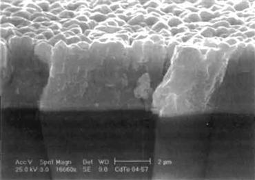
FIGURE 2 SEM image of the cross-section of a CdTe solar cell.
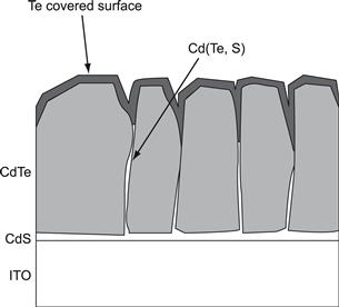
FIGURE 3 Schematic illustration of the key features of the CdTe solar cell.
2.2.1 The p–n Heterojunction—Improvement by Activation
Although both materials forming the junction are II–VI compounds and have a close chemical relationship, their lattice constants differ by about 5%. This leads to a significant density of interface states that can be expected to result in strong charge-carrier recombination. Junctions ‘as made’ indeed show low charge-carrier collection efficiency and thereby low-power efficiency of around 2%. Annealing of the system at temperatures of around 400 °C leads to some improvement, but only the still not completely understood ‘activation’ changes the junction so far that efficiencies of up to 16% have been observed. In this activation step, the junction is annealed at temperatures of 400–500 °C in the presence of Cl-containing species, generally CdCl2, which is deposited onto the film stack or admitted in vapour form for a time of around a few minutes. Figure 4 shows the strong improvement of the quality of the I–V curves under this treatment [2]. This procedure in the first instance has been developed quite empirically, although it is based on historic processes for the manufacture of CdS photoconductive films [3]. Only recently has light been shed on the basic processes that take place during activation. Three essential effects go hand in hand.

Recrystallisation—Grain Growth
Generally, for polycrystalline materials in which grain growth may occur, there is a limiting grain size in which the driving force is balanced by a retarding force. The net driving force decreases as the grain radius increases. Smaller grain sizes typically are observed for films grown at lower substrate temperatures due to lower mobility of atoms during growth. Upon annealing and activation, small grains can start to grow, but only to a certain limit. If, on the other hand, larger grains are formed already upon film deposition at higher deposition temperatures, such grains will grow less, as they are already closer to the final equilibrium. This has been observed experimentally: grain size in films deposited at 500 °C does not increase upon activation. Figure 5 shows that the grain diameter grows with distance from the junction—at which location nucleation of the films occurs—to an average size of 2 μm [4]. (The film has been deposited by CSS at 500 °C.) It does not change even under extended treatment times with CdCl2 species at 400 °C. This means that for these samples the grains were at equilibrium directly after material deposition, a satisfying situation. Figure 6 shows a TEM cross-section of a CdS–CdTe film stack deposited at a substrate temperature of 525 °C, indicating the typical morphology of such a system, clearly showing the high density and three-dimensional distribution of planar defects, mainly stacking faults and twins [5]. The density, however, varies from one grain to the other.

FIGURE 5 Grain-size distribution of a CdTe film as function of the distance from the junction after different thermal treatments [4].
For films deposited at significantly lower temperatures (<400 °C), the films show smaller grain sizes directly after deposition, together with strong orientation with the 111-axis perpendicular to the substrate. This orientation is lost upon recrystallisation during CdCl2 activation [6]. Figure 7, obtained by atomic force microscopy (AFM), shows directly three steps in the process of recrystallisation. During annealing under CdCl2, new small grains form on the highly oriented films and grow into the final unoriented phase, indicating close packing. The reference film deposited at 590 °C does not grow. The loss of preferential orientation upon annealing of this low-temperature film is strikingly illustrated in Figure 8 by X-ray pole diagrams by the same author [7]. The author attributes the grain growth and recrystallisation to lattice strain energy present in the films, which drives the process. In high-temperature–deposited films, no strain is present, leading to no significant recrystallisation. This strain present in low-temperature films is clearly illustrated by the author from an effective decrease of lattice constant: after (low-temperature) deposition, the lattice constant for a is 6.498 Å, which is reduced on activation to 6.481 Å, the published equilibrium value for crystalline powder.

FIGURE 7 Grain reconstruction in a CdTe film made at low temperature during activation (a, b, c) and unchanged film made by high-temperature CSS (d) [6].
(© American Institute of Physics.)
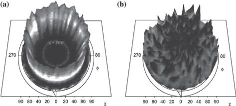
FIGURE 8 X-ray pole diagrams of 311 planes in a CdTe film: (a) before and (b) after activation at 400 °C V.
(© American Institute of Physics.)
In another study (Figure 9), grain-size distributions were measured [8] for films deposited at relative low temperatures directly after deposition (at 340 °C) and after annealing (at 580 °C) and alternatively after activation (at 430 °C). The final grain-size distribution has a maximum at 1 μm.

FIGURE 9 Grain-size distribution of a CdTe film directly after deposition, after annealing, and after activation [8].
(Reproduced with kind permission of James & James Publ.)
Immediately at the junction, where the film nucleates, some grain growth also has been observed for high-temperature films [9]. This region is difficult to access. More detailed knowledge may be crucial for an efficiency increase.
Interdiffusion—Intermixing
CdS and CdTe in thermal equilibrium may form mixed compounds CdSxTe1−x only for quite limited regions close to the single compounds, leaving a miscibility gap between x = 0.16 and x = 0.86 at 650 °C [10]. At lower temperatures, the gap widens. In the Te-rich region, the material shows a lower band gap than pure CdTe, an interesting feature in some II–VI compounds containing Te.
It is to be expected that CdS and CdTe intermix upon deposition at elevated temperatures to a certain degree. Intermixing at the interface can be expected to reduce the effects of lattice mismatch between CdS and CdTe. This can be analysed by secondary ion mass spectrometry (SIMS) depth profiling. SIMS analyses allow the elements to be determined quantitatively at the surface while it is removed layer by layer—e.g., by sputtering (‘depth profiling’). Such experiments have shown that intermixing of CdS and CdTe is a function of substrate temperature and postdeposition CdCl2 activation. The degree of intermixing indeed has been observed to increase with increase of substrate temperature. Further increase is induced by activation. Excessive interdiffusion leads to deterioration of the device performance. Spectral-response curves for devices made from CdTe films deposited at 610 °C and activated for different times are shown in Figure 10 [11]. Indeed the intermixing is manifest by a longer-wavelength response due to the lower-band-gap material for small values of x, the Te-rich mixture. This goes hand in hand with increased total photocurrent. Significant amounts of sulphur (probably CdSxTe1−x) can be detected both at grain boundaries and within heavily faulted grains (as opposed to grains with low-defect density) for films deposited at temperatures between 500 °C and 600 °C [5]. Model calculation yielded three-dimensional distributions of S and Te that have led to isocompositional contour plots of diffused regions [12] (Figure 11). In the case shown for two adjacent grains after activation, the different grain sizes result in a different alloy profile. For the narrower grain, no pure CdTe remains at all, while the wider grain exhibits the entire range of alloy composition. The evolution of mixed regions and their progression have been followed by X-ray diffraction studies, impressively showing the emergence of lines corresponding to mixed material. Figure 12 shows initially the line of pure CdTe and after 10, 20, and 40 minutes of activation the emergence and growth of alloy lines. Modelling of these results yielded diffusion coefficients that have been used to obtain the above three-dimensional profiles of Figure 11. Similar results have been obtained by measuring the lattice constant of films before and after activation [6]. The value for lattice constant a before annealing—as mentioned above—has a value of 6.498 Å (indicating stress in the CdTe film) and changes into two distinct values of 6.481 Å (relaxed CdTe) and 6.468 Å. The latter value does not occur for films deposited onto ITO film without any CdS. These results can only be explained by the occurrence of a CdSxTe1−x species with x = 0.2, corresponding to 6.468 Å.
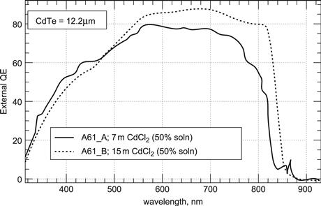
FIGURE 10 Illustration of intermixing of CdTe and CdS. by long-wavelength extension of sensitivity due to lower-band-gap mixed compound [11].
(Reproduced with kind permission of the Material Research Society.)
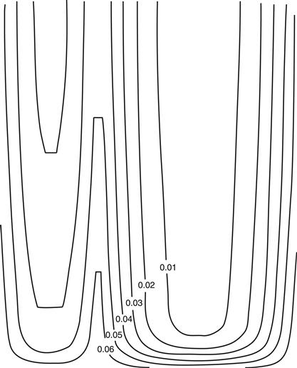
FIGURE 11 Simulated isocomposition lines of two grains in a CdTe/CdS film. Parameter = x in CdTexS1−x[8].
(© American Institute of Physics.)
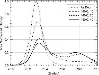
FIGURE 12 Emergence of mixed CdTe/CdS material after increased thermal stressing identified by X-ray diffraction [8].
(© American Institute of Physics.)
The presence of oxygen traces during CdTe film deposition usually is considered harmless, a fact that eases the requirements on vacuum equipment. Recently [13] it has been observed that oxygen leads to a reduced CdTe–CdS interdiffusion during activation, a fact that may reduce the danger of shunting of cells by CdS-enhanced grain boundaries, as illustrated in Figure 11.
Increase of Charge-Carrier Lifetime
Electrons generated as minority-carriers in the CdTe films have to reach (by diffusion) the field region at the junction and transverse the junction (by drift). Even under low-lifetime conditions, electrons generated directly at the junction can transverse the field region: the schubweg for an electron of 10 cm2/Vs mobility and a lifetime of 1 ns in an internal field of 104 V/cm of 1 μm with at a potential difference of 1 V i:μτE = 10−4 cm. If diffusion in the field-free region is required—for carriers created further away from the junction by red light—lifetime becomes more important. Moutinho et al. [14] have shown that CdTe films of good cells (11%) can show 2 ns lifetime. They have plotted efficiency of cells made similarly as a function of lifetime (Figure 13), allowing the conclusion that in CdTe solar cells diffusion of minority-carriers also plays an important role for achieving high efficiency.

FIGURE 13 Increase of efficiency of a cell by increase of minority-carrier lifetime [14].
(Reproduced with permission from IEEE.)
Conclusions on Activation
All these results indicate that major structural effects in CdTe solar cells occur upon the ‘magic’ activation process—namely, grain growth and interdiffusion, which are stronger for low-temperature deposited films than for films deposited at temperatures of 500 °C or more. These (‘high-temperature’) films directly lead to a stable structure with less recrystallisation and grain growth required.
The main effect of activation on efficiency of the devices, although, is an electronic improvement not so much by morphological effects but by improvement of the crystalline and electronic quality of grains immediately at the junction. Evidently, the lifetime of minority carriers in CdTe (electrons) determines the charge-carrier collection efficiency of the device.
2.2.2 The Back Contact
It is well known from semiconductor physics that it is not easy to contact a low-doped p-type semiconductor of relatively high energy gap. There are two general principles for making ohmic contacts to p-type semiconductors:
1. Use of a metal of work function higher than the electron affinity+energy gap of the semiconductor in order to align the top of the valence band with the Fermi level of the metal. The electron affinity+energy gap of CdTe is >6 eV. There is no metal of work function of >6 eV. This means that all metals lead to a blocking contact, as is illustrated in Figure 14, showing the band diagram of this situation.
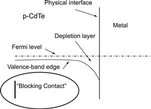
FIGURE 14 Energy band scheme of the metal–CdTe interface of a CdTe solar cell illustrating blocking contact.
2. Generation of a highly doped back-surface layer in the semiconductor. The unavoidable Schottky barrier created by the back-contact metal in the semiconductor will then be thin enough for holes to tunnel through efficiently. Figure 15 shows the band diagram for the second option, a highly p-doped surface region. Consequently, it remains to find practical solutions for this.
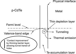
FIGURE 15 Energy band scheme of a metal contact to CdTe after generation of ap+ surface by Te enhancement leading to a thin barrier.
Efforts for high p-doping in CdTe usually fail due to a strong tendency for self-compensation of acceptors by formation of donors at elevated temperatures as used here. Furthermore, acceptors cannot be introduced by diffusion of atoms or ions from the surface, as diffusion preferentially proceeds along grain boundaries, leading to shunting of the cell by conducting grain boundaries before sufficient doping levels are achieved within the grains. In many cases, copper (an acceptor in CdTe) has been added—e.g., in graphite contacts still used for experimental contacting, which upon annealing can diffuse into the CdTe film. Its diffusion coefficient along grain boundaries is 100 times that in bulk CdTe [15]. If Cu reaches the junction, it first reduces the junction width and then compensates donors in the CdS layer. Recently, more stable contacts using Cu have been made by depositing Te–Cu double films, which can react to produce Cu2Te compound films upon annealing, some of the Cu diffusing into the CdTe film and leading to a minute surface doping [16].
Alternative efforts in the past have been directed primarily toward three semiconductors: HgTe, ZnTe:Cu, Te and Cu2Te [17,18]. All of them have led to unstable contacts.
It has become obvious in the course of recent work [4] that a stable back contact cannot consist simply of a metal film. A new contact system has been developed, consisting of a triple procedure [4]:
• generation of an accumulation layer (e.g., by suitable etching of CdTe, a Te-enhanced surface layer can be generated);
• deposition of a p-type narrow-band-gap, chemically inert semiconductor or semimetal (buffer layer);
• deposition of a metal film for low-resistance current collection (metal contact).
The role of the buffer layer essentially consists of protecting the (chemically sensitive) p-type accumulation layer from being corroded by the (reactive) metallic current-collection film. All three components had to be individually optimised and mutually adjusted. Such a triple structure can be highly stable and made by using techniques suited to large-scale production.
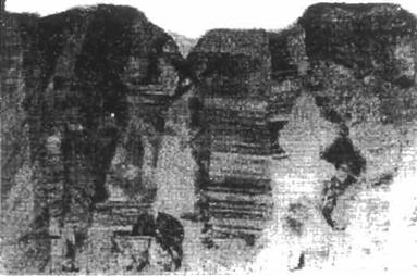
The etching process used proceeds into the grain boundaries, leading to ‘Te caps’ covering the grains as illustrated in Figure 3. This has been strikingly visualised experimentally [17] by sputter-etching away the first 30 nm of the film and analysing the new surface by scanning Auger analysis. Figure 16 clearly shows grain boundaries having excess Te in the form of lighter-coloured regions.
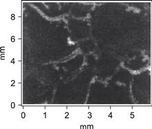
FIGURE 16 Te-capped CdTe grains by scanning EDX analysis of an ion milled back surface (light areas are Te-enhanced) [7].
(Reproduced with permission from IEEE.)
2.3 Stability Issues
Due to the material’s strong ionicity (72%), the energy of the bond between Cd and Te is quite high (5.75 eV) [18]. The energy of any photon in the solar spectrum is lower than the binding energy in CdTe or CdS, so breaking of bonds must not be considered. The strong bonding leads to an extremely high chemical and thermal stability, reducing the risk of degradation of performance or any liberation of Cd to a very low level. No degradation intrinsic to the material can be expected.
The stability risks of back contacts have been virtually eliminated by the triple structure described in Section 2.2.2. Nevertheless, careful process development has to be performed to avoid stability risks from other processing steps such as influences of additives in the lamination material. Only dedicated tests of products can yield to assured stability of the product.
2.4 Best Performance of Cells
Using the most advanced techniques, record efficiencies have been achieved by a few groups, indicating the potential of the CdTe thin-film solar cell. In 1984 the magic limit of 10% efficiency was surpassed by a group at Kodak laboratories, using close-spaced sublimation (CSS) [19]. In 1993, an efficiency of 15.8% was achieved [20] by a group from the University of South Florida that used CSS again for formation of CdTe films on borosilicate glass at temperatures of around 600 °C. Fine-tuning has been achieved using CdS films made by chemical bath deposition and finally applying an antireflection coating onto the glass surface positioned toward the sun. This value could be surpassed only 7 years later by a group from National Renewable Energy Laboratory (NREL), which achieved 16.5% efficiency [21]. The important advance in this work has been the use of CdSnO4 deposited onto borosilicate glass.
In both recent cases, the higher deposition temperature allowed by use of (expensive) borosilicate glass has been a central issue. For industrial production, this type of glass is presently considered too expensive. Therefore, in industrial production, low-cost soda-lime glass is used, which is limited in temperature endurance.
3 Making of Integrated Modules
3.1 Interconnection of Cells
Semiconductor solar cells are devices delivering open-circuit voltages of less than 1 V. As electric power for commercial applications requires higher voltages, it has proven advantageous to connect a multitude of cells in series in ‘modules.’ Whereas in the case of silicon solar cells, individual cells have to be series connected by conductors welded onto both sides of wafers, thin-film cells have a strong advantage to allow integrated series connection of numerous cells, which are at the same time defined in area and interconnected. If the different layers of the cells—TCO, p–n film stack, and back contact—are individually separated (scribed) into parallel stripes that overlap asymmetrically the series, then connection of one distinct cell with its neighbour can be achieved periodically for all cells so generated, as illustrated in Figure 17. After deposition of the TCO film, a first set of separation scribing lines at a periodic distance of about 1 cm is applied, typically by laser ablation. Subsequently, the p–n film sandwich is deposited and separated at the same periodicity so that this scribing line opens the TCO beneath for the back contact, which is deposited subsequently. If the back contact now is separated by a similar set of lines at a small distance from its contact line to the TCO, the interconnection is achieved. Figure 17 shows the principle for a set of three cells.
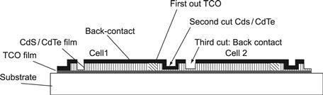
FIGURE 17 Interconnection principle.
In some cases, such as electrodeposition, it is not permissible to separate the TCO film before depositing the semiconductor film. Here a variation in the procedure allows the scribing of the first two lines after the deposition of the semiconductor film [22]. An insulating fill-up of the first scribing line is required in this process, as illustrated in Figure 18.

FIGURE 18 Modified interconnection principle.
Evidently, using these techniques, the cell width can be adjusted according to technical needs or commercial requirements, On one hand, more interconnection triple scribes lead to higher loss in active area. (Typically, a scribing system requires between 0.2 and 0.3 mm.) On the other hand, wider cells will lead to increased series resistance (lower fill factor), as the current density being conducted through the TCO film will be higher, leading to higher voltage drop. For CdTe, a cell width of 9–10 mm seems to be an optimum value for TCO films of 8–10 Ω per square resistivity. (For CIS cells, due to higher current density and lower voltage of the individual cell, smaller cells—about 6 mm wide—are appropriate; conversely, for amorphous silicon, wider cells are optimal.)
3.2 Contacting
The photocurrent of a module transverses all series-connected cells and is extracted by contacts to the first and last cell; all individual cell voltages add to the total voltage. Usually, metallic conductors are attached to the free contact area of the first and last cell by conducting adhesive and are further connected by contact bands toward the point of the module, where it transverses the back sealing, typically glass. Usually the contact bands are Sn-plated Cu ribbons. Figure 19 indicates the topology of the contacting conductors. Care has to be taken to avoid shunting at any place.

FIGURE 19 Topology of contact bus system, as seen from the back of the module.
3.3 Lamination
After contact-bus attachment, the module needs sealing and protection against external influences. This usually is achieved by laminating a second glass plate to the module-carrying side of the first glass plate. It is required to remove all films at a boundary region of 1–2 cm of the module to provide the required electric insulation of the module. This is usually achieved before contacting by sandblasting or laser ablation.
For historical reasons, in many cases the technology used for silicon modules is also used for CdTe modules—namely, sealing by EVA (ethyl-vinyl-acetate), which is used as a monomer, applied as a sheet, and polymerised by a thermal annealing step under vacuum. Commercial EVA is readily available. It is ‘overqualified’ for CdTe, as intense development work has been invested into the commercial product to stabilise it against degradation in the sunlight impinging onto silicon modules. In the case of CdTe, this special quality is not required, because sunlight directly enters the junction after having passed the glass and the lamination material is positioned below the second glass and therefore oriented away from the sun.
The cover glass so laminated to the module has a hole through which the contact bands are guided into a contact box, which is attached to the glass (cf. Figure 19). Two stable current guides with plugs are attached to the box and will be used for connecting the modules so generated to the user circuit. Evidently, all connections and contacts must be extremely well protected against water and water vapour for achieving the expected lifetime of the module.
4 Production of CdTe Thin-Film Modules
4.1 Generalised Production Sequence
The different steps to make cells and modules described in Sections 2 and 3 can be arranged into a sequence to make ready-to-use modules as a product:
1. selection of substrate glass, soda-lime glass (float glass) as substrate;
2. deposition of the transparent conductive coating (SnO2, ITO, etc.);
3. scribing of the TCO film into parallel bands, defining and separating the cells (for some processes, this scribing can be done later after deposition of the semiconductor films);
4. deposition of CdS films of lowest possible thickness, typically around 100 nm;
5. deposition of CdTe by the process of choice for the particular product;
6. activation of the film stack by influence of CdCl2 at temperatures of around 400 °C;
7. application of the second scribing step, which opens the semiconductor stack for contacting the TCO film (optionally, step 3 can be applied in parallel; the scribing line afterward has to be filled up for electrical insulation);
8. application of the back-contact structure, consisting of a set of steps—e.g., etching to achieve a Te accumulation, application of a buffer layer, application of the metallic back contact;
9. separation cut to separate the back contacts of the neighbouring cells;
10. attachment of the contact-bus structure;
11. lamination with a second glass (or plastic) using a suitable plastic such as EVA or a thermoplastic film, the contacts protruding through a hole in the cover glass plate for the next step;
12. contact-box attachment in which the fragile contact bands from the module are connected to stable cables with suitable plugs for commercial application; and
13. measurement of each module’s efficiency using a solar simulator.
With some modifications, this sequence is the basis of the following industrial efforts into production.
4.2 Industrial Production of Modules
A commercial product can only be manufactured with expectation of cost-covering revenues, if a factory above a certain capacity is built, using the dimensions of scale. It is generally accepted today that a capacity of around 100,000 m2 per annum is presently appropriate. All units of significantly lower capacity should be called pilot plant as they will require more funds than any return can provide. At around 600,000 m2 per annum a cost potential of 0.6/Wp has been estimated by a group of experts [23].
Presently three industrial units are known to actively pursue the target of large-scale production. They basically differ by the deposition technique for CdS and CdTe.
4.2.1 BP Solar Inc. (Fairfield, California, USA)
Work at BP Solar started in Great Britain in 1984 when British Petroleum took over a galvanic deposition process for CdTe thin-film solar cells from Monosolar Inc. in the United States. BP Solar continued development of the basic electrodeposition process for CdTe [24]. Upscaling work resulted in a factory built in the United States. Due to low deposition rates, parallel deposition is used: a large number (40 to 100) of plates are immersed into a tank containing a recirculation system for the continuously replenished electrolyte. A constant potential is applied to the plates via the TCO films already covered by CdS. (The CdS film is deposited by the chemical bath deposition technique, also in parallel onto a larger number of TCO-coated glasses.) The total charge applied to the plates is a measure for film thickness. A charge of about 12,000 C/m2 leads to approximately 1.6 μm of CdTe film. Postannealing leads to strain relief, change of conduction polarity from n to p, and activation by means of a Cl compound added to the bath. The grain size grows from 0.1 to 0.2 μm to about 0.4 μm during this procedure.
Great care has to be taken to avoid lateral voltage drop over the plate surface during CdTe deposition. Te- or Cd-rich compounds can form upon deviation from this condition. To achieve good-quality films, the lowest possible surface resistivity of the TCO has to be chosen. The cell-defining and module-generating scribe application follows the principle shown in Figure 18. In order to keep the TCO film intact as long as possible, the TCO scribing lines are applied after CdTe deposition, necessitating a fill-up procedure. Module sizes are around 1 m2, yielding a power of around 72 W under simulated terrestrial solar light, have been reported [25]. More than 150,000 m2 of glass substrates can be processed per annum. The line can produce 0.55-m2 and 0.94-m2 modules. The deposition system consists of eight identical deposition tanks. Each tank is able to simultaneously coat forty substrates of 0.55-m2 or twenty-four of 0.94-m2. Since 2002, BP Solar has manufactured the first large area CdTe module of >10% efficiency.1
4.2.2 First Solar LLC (Toledo, Ohio, USA)
This company started work within the scope of a predecessor called Solar Cells Inc. around 1991 in Toledo by a senior shareholder of Glasstech Inc. In 1999, a joint venture with a finance group from Arizona was formed that led to the new name First Solar LLC [26]. The basic process for generating CdS–CdTe junctions relies on the sublimation and condensation properties of CdS and CdTe described earlier. Substrates coated by SnO2 films by Libbey Owens Ford using a spray process enter a vacuum system through a loadlock and move—lying on a roller system to avoid warping—into a chamber heated to temperatures around 560 °C. Vapour sources are positioned above the substrates out of which CdS and CdTe vapours emerge, are directed toward the substrates, and condense sequentially on the substrates. The CdS and CdTe material is continuously fed into the evaporators. Module interconnection of cells is performed afterward—i.e., first and second scribing lines are applied after semiconductor deposition, requiring filling of scribing line 1 (cf. Figure 18).
The standard module size of First Solar is 60×120 cm2 = 0.72 m2[27]. Efficiencies of 6–8% can be routinely achieved. Figure 20 shows area efficiency versus sequential plate count for 3128 sequentially deposited modules.

FIGURE 20 Total-area efficiency for 3128 sequentially deposited modules from First Solar LLC
(from [27]).
4.2.3 ANTEC Solar GmbH (Arnstadt, Germany)
The technology used at ANTEC Solar is essentially based on the development started at Battelle Institute around 1970 [28]. After the closure of Battelle Institute, the know-how was transferred to ANTEC GmbH, a management buyout from Battelle, and developed into a manufacturing technology. ANTEC Solar was founded in 1996 in order to start production of CdTe thin-film PV modules. A fully automated production plant has been built in Arnstadt (Germany), and production started in 2001. The basic process used for deposition of CdTe is close-spaced sublimation. Glass substrates carrying scribed TCO films are transported in vacuum above crucibles containing CdS and CdTe at temperatures of 700 °C. The semiconductor materials condense at temperatures of 500 °C and form the n–p diode structure, which is activated in a CdCl2 atmosphere. Module size is 60×120 cm2; module efficiencies were about 7% and were expected to increase to 8% in 2002. In contrast to BP Solar and First Solar, the TCO is also made in the plant in the online system. Definition of interconnected cells is achieved according to Figure 17—i.e., at three different stages of the plant by laser ablation (first scribe) and mechanical ablation (second and third scribe).2
Figure 21 shows the total area efficiency of 2000 modules manufactured in one production run. The production plant presently employs 100 persons.
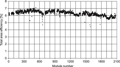
FIGURE 21 Total area efficiency for 2000 sequentially deposited modules from ANTEC Solar GmbH.
4.3 A 10-MW Production Line
The following uses an example to describe and illustrate the production line of ANTEC Solar GmbH.
The deposition line was conceived as a two-step production line consisting of a fully automated deposition line for integrated modules on glass substrates of 60×120 cm2 and a semiautomatic module line for hermetical sealing, contacting, measuring, and customising of the modules into a marketable product.
The fully automatic in-line deposition procedure consists of nine steps:
1. Cleaning of the substrate (float glass).
2. Deposition of the transparent contact (ITO+SnO2) at around 250 °C.
3. Scribing of the TCO film for cell definition and interconnection.
4. Deposition of CdS and CdTe by CSS at around 500 °C.
5. Activation (improvement of junction by annealing in Cl-containing atmosphere at around 400 °C).
6. Wet-chemical etching for contact preparation (Te accumulation).
7. Scribing by mechanical tools for interconnection of cells.
8. Deposition of two-layer back contact by sputtering.
9. Scribing by mechanical tools for separation and interconnection of cells.
Most of these positions are connected by heating or cooling segments in order to present the plates to the deposition steps at the adequate temperatures They take a large part of the equipment length. The highest temperature (500 °C) is reached during deposition of the semiconductor films, compatible with glass stability. The total length of the automated deposition line is 165 m. Glass plates (to become modules) are transported by automated conveyor systems and are not touched by human hands during the processes. They are collected in boxes in sets of 30 and transferred to the module line in an adjacent hall.
In the module line, the substrates with sets of interconnected cells (often called submodules) are contacted and sealed for convenient use in energy-generating systems. This part of the factory consists of the following procedures:
1. Cleaning of the cover glass (float glass).
2. Deposition of the contact buses onto the modules.
3. PV function testing to identify substandard modules, which can be excluded from further processing.
4. Cutting of EVA sheet to size.
5. Joining of module, EVA sheet, and cover glass.
6. Lamination (sets of six modules).
7. Fill in of contact hole in cover glass.
9. Quantitative measurement of PV performance (sets of three modules).
The module line requires some manual handling and adjustments due to the heterogeneity of the processes. Figure 22 shows the geometrical arrangement of the different processes. Each line has been installed in a separate hall. Both halls are connected by an aisle for transfer of modules. Buffer stations allow the removal of partly completed modules in case of an incident in the downline stations without crashes in the upline stations. The overall primary parameter for the deposition line and also the module line has been the production speed defined at 120,000 modules per annum, which leads to an average linear transportation speed of approximately 1 m/min in the production line.

FIGURE 22 Schematic of the components of the plant.
The procedures described above contain (1) state-of-the-art procedures, (2) new but simple procedures, and (3) newly developed procedures.
Standard procedures are sputter deposition of ITO and SnO2 metals. Dedicated equipment has been constructed by experienced equipment manufacturers. In some cases (e.g., ITO deposition), multiple sputtering targets are needed in order to achieve the required film thickness at the given transport speed of the substrates (around 1 m/min). The final steps of contacting and lamination are also using state-of-the-art techniques. Equipment can be bought custom-made on the market. An unforeseen effort in the setup and initial operation of the plant had to be dedicated to the transport of the substrate sheets through heating and cooling stages without breakage due to excessive thermal gradients. After some significant modifications, breakage under thermal stress could be virtually eliminated.
Simple but new processes are essentially the core processes for the active semiconductors, namely, CSS deposition of CdS, CdTe, and—if required—back-contact buffer semiconductors. It has been shown that CdTe can be deposited onto stationary substrates at rates of 10 μm/min and more. For achieving the required production speed, three crucibles containing a week’s supply of starting material of CdTe are used. For CdS, due to its low thickness, only one crucible is used. As mentioned, the vacuum requirements are rather low, so no high-vacuum equipment is needed. (For CdTe, oxygen incorporation to some extent indeed is considered advantageous by some researchers.) Laser scribing of the TCO film does not require basic new technologies. Equipment can be built by industry, and processing data have to be developed and adjusted. In spite of these arguments, some problems have been incurred by thermal stress conditions of crucibles and substrates. Fast heating invariably leads to breakage of glass substrates.
More involved new processes are activation of the junction CdS–CdTe and etching of the CdTe surface as a contact-preparation procedure. Etching requires the wetting of the substrates carrying the activated CdS–CdTe film stacks by nitric and phosphoric acid plus water solutions (NP etch), rinsing, and drying. Although being essentially simple, procedures equipment had to be developed to incorporate these processes under tightly controlled parameters into the production line to allow the target speed to be achieved. Activation requires exposition of the substrates carrying the TCO-CdS-CdTe film-stack to, e.g., CdCl2 at elevated temperatures. Fortunately, traces of oxygen do not play a detrimental role. (The activation step in the laboratory can even be executed in air.) Furthermore, CdCl2 at room temperature has extremely low vapour pressure. Some special chemical-engineering skill has been needed to conceive an in-line activation stage fitting into the production line. Mechanical scribing has turned out to be more involved, due to the requirement that the production line should have only one service interval per week. Scribing tools have to survive one week under tough tolerances. New solutions had to be found for recognising and identifying the first laser cuts below the CdTe film for precise positioning of the second and third scribing lines. Implementation of automatic image recognition of previously scribed lines in the TCO films for precise positioning of subsequent scribing lines has been a nontrivial task.
After the plant had been built and assembled in 1999 and the first functional tests had been passed in early 2000, debugging and process optimisation required extensive tests and equipment modifications by hardware and software manufacturers. Production started in 2001. Figure 23 shows the deposition line in its entirety.
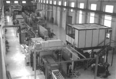
FIGURE 23 View of the total deposition line.
4.4 Environmental and Health Aspects
The production of polycrystalline thin-film CdTe solar modules basically employs techniques common in chemical and microelectronic industry. The substances involved are easily manageable by standard processes. Production is possible under existing safety laws without putting staff health at risk. It is technically and economically possible to design and operate a factory with zero emissions. Workers in a production environment have been tested regarding Cd uptake and shown Cd content in blood and urine far below the threshold concern level under periodic medical scrutiny [29]. Smokers have shown a somewhat higher Cd level than do nonsmokers but still are below any threshold for concern.
A number of studies from third parties [30–33] show negligible risk under use of CdTe solar modules for the environment and humans even under irregular conditions. In case of exposure to fire, the substrate and cover glass will melt long before the CdTe decomposes, thereby including the semiconductor into the resolidifying glass. Incineration experiments conducted by BP Solar in cooperation with a fire research institution using typical household inventory plus CdTe modules have not led to detectable emissions of Cd compounds [30].
During use, a CdTe module can be compared to laminated glass similar to that used in cars. Thus, modules will not easily break and release their content. At their end of life, modules can be recycled by crushing them whole and either returning the debris to the smelters, which can inject the material into their processes without significant additional cost, or dissolving the films by liquid or gaseous etchants.
Debis Systemhaus GmbH (a subsidiary of Daimler-Chrysler AG) has established a life-cycle inventory for CTS thin-film solar modules of ANTEC Solar GmbH guided by ISO 14040 and 14041. To achieve this aim, the total energy and material flow for the module’s life cycle has been accounted with help of the CUMPAN® software system. This allows, for example, the determination of the total energy required for raw materials’ production and processing.
• The manufacture of 1 m2 of CTS-module uses 126 kg of raw material and primary energy carrier and 70 kWh of electric energy.
• Under the climatic conditions of Germany, the generation of 1000 kWh of electricity per annum at a module lifetime of 30 years saves 16,244 kg of carbon dioxide and further undesired materials such as sulphuric dioxide and nitrogenic oxides.
• The production plant is built not to emit any material. Water is reprocessed and reused. (Waste heat, however, is emitted to the environment at this time.)
• A recycling process is envisaged for spent and reject modules. In view of environmental safety, economical retrieval of valuable raw materials, and securing of hazardous materials, this process can be considered satisfying.
• Compared with alternative thin-film modules (a-Si, CIS), emissions and waste during production amount to similar values.
• The emission of cadmium can be judged as low in comparison to other emission sources (e.g., coal-fired power plants, phosphate fertiliser). Even in case of accidents (e.g., fire), by reason of the small quantities of (thermally stable) material per square metre of module area, no environmentally critical emission must be contemplated.
• The total energy used for fabricating a module will be retrieved by the module within 15 months using the actual energy uptake of the ANTEC factory. From then on, the module operates in an environmentally benign way.
4.5 Material Resources
More than 99% of the weight of a CdTe modules consists of float glass, EVS, and metal connectors readily available in virtual unlimited quantities. TCO films made of SnO2 are not considered to be limited by available Sn supplies. In used in ITO films is a more rare resource at an annual production of 120 t [34]. Furthermore, it is also used for ITO films in liquid crystal displays and the CuInSe2-based thin-film solar cell. ITO can be substituted by SnO2 and—possibly—ZnO, Sn and Zn being abundant metals. CdTe and CdS warrant a closer consideration. Presently, CdTe (and CdS) are offered in the required purity by five industrial enterprises. Cd is presently produced as a by-product of Zn at 20,000 t per year [34]. Due to low demand, Te is presently produced at 300 t per year as a by-product of Cu [34]. Growing future demand, according to an expert in the field [35], can be satisfied by more efficient extraction from the anodic slurries in Cu electrorefining and also by exploiting Te-rich ores in South America not yet exploited. S finally is an abundant element.
In summary, no critical material bottleneck is expected for an expanding production. The CdTe thin-film solar cell will be able to take a share in ameliorating future energy shortages and the climate change expected from burning fossil fuels.
5 The Product and Its Application
The photovoltaic modules manufactured in a factory are ready to use in a suitable PV installation. CdTe modules by any one manufacturer are mass products made on large scale (100,000 per year or more). Typically, the modules are sized about 0.6×1.2 m2. A module 60 cm wide can easily be carried under the arm by one person. Glass–glass laminates, as manufactured, for example, by First Solar and ANTEC Solar, have a weight of 16 kg. A contact box furnishes two cables carrying plugs (male and female for easy series connection) that are long-term stable. Figure 24 shows an ATF module from ANTEC Solar. A very homogeneous appearance of most thin-film modules helps organic and visually pleasing installation.

FIGURE 24 View of a CdTe thin-film PV module.
5.1 Product Qualification
A PV module is a product made for long-time deployment in a harsh environment and therefore must be furnished with a warranty for approximately 20 years of useful life. In order to provide such assurance, the international standards agencies (International Electrotechnical Commission, or IEC) have designed international norms that are valid worldwide. The norm pertaining to thin-film modules is IEC 61646, ‘Thin film terrestrial photovoltaic modules -Design qualification and type approval.’ This norm was published in 1996 and was originally designed with amorphous silicon modules in mind.
Modules to be classified as fulfilling IEC 61646 have to undergo an extensive set of tests defined in detail in the text of this norm. Briefly these are four sets, for which eight modules have to be provided, typical for the production discussed:
5.2 Examples of Installation of CdTe Modules
Thin-film modules can show a highly homogeneous surface appearance and very little variation from module to module. This allows the assembly of large, highly homogeneous panels on rooftops, on facades, or on the ground. Figures 25–27 show examples of such installations. Modules in the form of glass–glass laminates can be mounted on special structures, which can be invisible and nonetheless watertight. Figure 28 shows how modules can be mounted on metal rafters that allow water drainage and also seal the interior of the roof by rubber lips.
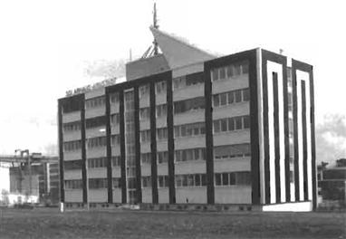
FIGURE 25 Installation of CdTe modules from First Solar LLC on an office building.

FIGURE 26 Installation of CdTe modules from ANTEC Solar on the wall of a public administration building.
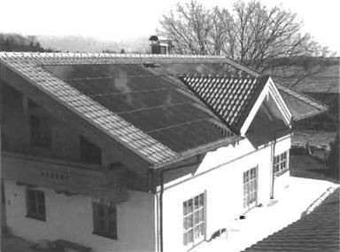
FIGURE 27 Installation of CdTe modules on a private residence roof.
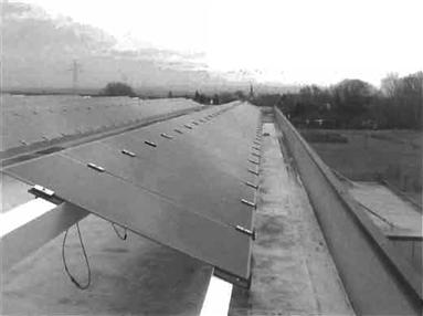
FIGURE 28 Close-up of mounting system on metal rafters for roof installation.
6 The Future
After more than 20 years of development in various industrial and academic laboratories, the CdTe thin-film solar module has entered the production stage, and experience is being gained in this process. This will definitively lead to the next generation of plant at capacities around 1,000,000 m2 per year. It is expected that the learning curve will be transgressed quite quickly, which will lead to a mature low-cost product.
References
1. K. Zanio, Cadmium telluride: materials preparation, physics, defects, applications, in: Semiconductors and Semimetals, vol. 13, 1978.
2. D. Bonnet, et al., The CdTe thin film solar cell—EUROCAD, in: Final Report to the Commission of the European Communities, Project No. JOU2-CT92–0243, 1995. Referenced data later also published in: H.M. Al Allak, et al., The effect of processing conditions on the electrical and structural properties of CdS/CdTe solar cells, in: Proceedings of the 13th European Photovoltaic Solar Energy Conference, Nice, 1995, pp. 2135–2138.
3. Bube R. Photoconductivity of Solids. New York, London: Wiley; 1960; p. 94.
4. Bonnet D, et al. CADBACK: The CdTe thin film solar cell—improved back contact. In: Final Report to the European Commission, Contract No JOR3-CT98– 0218. 2002;.
5. Dhere R, et al. Influence of CdS/CdTe interface properties on the device properties. In: Proceedings of the 26th IEEE Photovoltaic Specialists Conference. 1997;:435–437. Anaheim.
6. Moutinho RH, et al. Effects of CdCl2-treatment on the recrystallization and electro- optical properties of CdTe films. J Vac Sci Technol A16 1998;:1251–1257.
7. Moutinho HR, et al. Alternative procedure for the fabrication of close-spaced sublimated CdTe solar cells. J Vac Sci Technol A18 2000;:1599–1603.
8. McCandless B, Birkmire R. Diffusion in CdS/CdTe thin-film couples. In: Proceedings of the 16th European Photovoltaic Solar Energy Conference. 2000;:349–352. Glasgow.
9. K. Durose, Private communication.
10. Nunoue S-Y, Hemmi T, Kato E. Mass spectrometric study of the phase boundaries of the CdS/CdTe system. J Electrochem Soc. 1990;137:1248–1251.
11. Dhere RG, et al. Intermixing at the CdS/CdTe interface and its effect on device performance. Mat Res Soc Symp Proc. 1966;426:361–366.
12. McCandless B, Engelman MG, Birkmire RW. Interdiffusion of CdS/CdTe thin films: modelling X-ray diffraction line profiles. J Appl Phys. 2001;89:988–994.
13. Yan Y, Albin DS, Al-Jassim MM. The effect of oxygen on junction properties in CdS/CdTe solar cells. In: Proceedings of the NCPV Program Meeting. 2001;51–52.
14. Moutinho HR, et al. Study of CdTe/CdS solar cells using CSS CdTe deposited at low temperature. In: Proceedings of the 28th IEEE Photovoltaic Specialists Conference. 2000;646–649. Anchorage.
15. Hegedus SS, McCandless BE, Birkmire RW. Analysis of stress-induced degradation in CdS/CdTe solar cells. In: Proceedings of the 28th IEEE Photovoltaic Specialists Conference. 2000;535–538. Anchorage.
16. Hegedus SS, McCandless BE, Birkmire RW. initial and stressed performance of CdTe solar cells: effect of contact processing. In: Proceedings of the NCPV Program Review Meeting. 2001;119–120.
17. Levi DH, et al. Back contact effects on junction photoluminescence in CdTe/CdS solar cells. In: Proceedings of the 26th IEEE Photovoltaic Specialists Conference. 1997;351–354. Anaheim.
18. Hartmann H, Mach R, Selle B. Wide gap II–VI compounds as electronic materials. In: Kaldis E, ed. Current Topics in Materials Science. 1981;1–414. Amsterdam.
19. Tyan Y-S, Perez-Albuerne EA. Efficient thin film CdS/CdTe solar cells. In: Proceedings of the 16th IEEE Photovoltaic Specialists Conference. 1982;794–800. San Diego.
20. Britt J, Ferekides C. Thin film CdS/CdTe solar cell with 15.8% efficiency. Appl Phys Lett. 1993;62:2851–2852.
21. Wu X, et al. 16.5% efficient CdS/CdTe polycrystalline thin film solar cell. In: Proceedings of the 17th European Photovoltaic Solar Energy Conference. 2001;995–1000. Munich.
22. Rose D, et al. R&D of CdTe-absorber photovoltaic cells, modules and manufacturing equipment: plan and progress to 100MW/yr. In: Proceedings of the 28th IEEE Photovoltaic Specialists Conference. 2000;428–431. Anchorage.
23. Woodcock JM, et al. A study on the upscaling of thin film solar cell manufacture towards 500MWp per annum. In: Proceedings of the 14th European Photovoltaic Solar Energy Conference. 1997;857–860. Barcelona.
24. Cunningham DW, et al. Advances in large area apollo module development. In: Proceedings of the NCPV Program Review Meeting. 2000;261–262.
25. Cunningham DW, et al. Large area appollo thin film module development. In: Proceedings of the 16th European Photovoltaic Solar Energy Conference. 2000;281–285. Glasgow.
26. McMaster A, et al. PVMat advances in CdTe product manufacturing. In: Proceedings of the NCPV Program Review Meeting. 2000;101–102.
27. Rose D, Powell R. Research and progress in high-throughput manufacture of efficient, thin-film photovoltaics. In: Proceedings of the NCPV Program Review Meeting. 2001;209–210.
28. Bonnet D, Rabenhorst H. New results on the development of a thin film p-CdTe– n-CdS heterojunction solar cell. In: Proceedings of the 9th IEEE Photovoltaic Specialists Conference. 1972;129–131. Silver Springs.
29. Bohland JR, Smigielski K. First solar’s module manufacturing experience; environmental, health and safety results. In: Proceedings of the 28th IEEE Photovoltaic Specialists Conference. 2000;575–578. Anchorage.
30. Alsema EA, van Engelenburg BCW. Environmental risks of CdTe and CIS solar cell modules. In: Proceedings of the 11th European Photovoltaic Solar Energy Conference. 1992;995–998. Montreux.
31. Patterson MH, Turner AK, Sadeghi M, Marshall RJ. Health, safety and environmental aspects of the production and use of cdte thin film photovoltaic modules. In: Proceedings of the 12th European Photovoltaic Solar Energy Conference. 1994;951–953. Amsterdam.
32. Moskowitz PD, Steinberger H, Thumm W. Health and environmental hazards of CdTe photovoltaic module production, use and decommissioning. In: Proceedings of the First World Conference on Photovoltaic Energy Conversion. 1994;115–118. Hawaii.
33. Steinberger H. Health and environmental risks from the operation of CdTe- and CIS thin film modules. In: Proceedings of the 2nd World Conference on Photovoltaic Solar Energy Conversion. 1998;2276–2278. Vienna.
34. US Bureau of Mines. Mineral Commodity Summary. 1992.
35. G. Daub, PPM Pure Metals GmbH., personal communication.
1.In 2002, the management of BP Solar decided to terminate its CdTe development and production efforts after 18 years of investment and closed down the factory.
2.Because of financial problems. ANTEC Solar declared insolvency in 2002. In 2003, the plant was taken over by a new owner, who successfully restarted production.