Chapter ID-2
Organic Solar Cells
Chapter Outline
2. Organic Electronic Materials
2.1. Excitons in Organic Semiconductors
3. Principles of Device Operation
3.3. Bulk Heterojunction Architecture
4. Optimising Solar Cell Performance
4.1. Optimising Light Harvesting
4.3. Optimising Voltage Generation
4.4. Optimising Electrodes for Voltage Generation
4.5. Organic Tandem Solar Cells
4.6. Optimising Microstructure of Bulk Heterojunctions
5.4. Degradation of Morphology
1 Introduction
The discovery of a photovoltaic effect from organic materials [1–2] has led to an intense stimulation of research interest. Organic semiconductor materials offer the potential for low-cost and low-temperature preparation methods, mechanical flexibility, colour tuning, and the ability to be deposited on a wide variety of substrates, resulting in a widening of the range of applications of photovoltaic technology. The expected low capital cost for manufacture of organic photovoltaic (OPV) modules makes OPV technologies scalable and therefore suitable for distributed power applications.
Organic solar cell efficiencies have undergone a drastic acceleration in performance since the last edition of this book. At the time of this writing, the record power-conversion efficiency for solar cells with an all-organic active layer is 8.3%; this record has been achieved both for a polymer–fullerene blend deposited from solution [3] and for a blend consisting of two nonpolymeric semiconductors, deposited under vacuum [4]. These results represent almost a doubling of efficiency in the past 5 years.
1.1 Moving Toward the Market
Despite the impressive recent advances in device performance, further improvements, particularly in the performance of cost ratio through advancements in efficiency (with a goal of $1 per watt generated) and in device stability, are required to convert these laboratory-scale achievements into commercial reality. However, the prospect of cheap organic solar power is coming closer, and a small number of OPV products have already been brought to market, mostly for charging applications (e.g., Konarka’s Power Plastic range [5]). The acceleration in this field in the commercial sector is evident in the increasing number of newly launched companies and existing materials or device manufacturers who have added organic photovoltaics to their portfolios.
The remainder of this chapter outlines the current understanding of organic photovoltaics and the key challenges that must be addressed in order to deliver on the promise of plastic solar power.
2 Organic Electronic Materials
The materials used in organic solar cells are classed as organic semiconductors as a consequence of their ability to absorb light and conduct charge, either within the molecules (such as in conjugated polymers) or through a molecular network. Conjugated polymers that have been studied in photovoltaic applications include polythiophenes, poly-phenylene-vinylenes (PPVs), polyfluorenes, and polycarbazoles, whereas nonpolymeric (‘small molecule’) organic semiconductors used in organic photovoltaic devices include functionalised fullerenes, phthalocyanines, perylene derivatives, and pentacene. Figure 1 shows examples of these conjugated materials. The desirable properties of visible absorption and charge transport in conjugated organic molecules arise from the network of π bonding between unsaturated atoms (largely carbon). The carbon atoms in the conjugated sections of the molecule form strong σ bonds using three sp2 orbitals, whereas the p orbitals lying perpendicular to the plane of the molecule are able to form π bonds, which are less tightly localised than the strong σ bonds. Increasing conjugation across several atoms allows delocalisation of the π orbitals (in conjugated polymers, this typically extends over 2–10 repeat units), which may support the conduction of charge.
FIGURE 1 Selected organic photovoltaic materials: (a) poly-3-hexyl thiophene (P3HT); (b) poly[2-methoxy-5-3(3´,7´-dimethyloctyloxy)-1-4-phenylene vinylene](MDMO-PPV); (c) poly[N-9´-hepta-decanyl- 2,7-carbazole-alt-5,5-(4´,7´-di-2-thienyl-2´,1´,3´-benzothiadiazole)] (PCDTBT); (d) poly((9,9-dioctylfluorene)-2,7-diyl-alt-[4,7-bis(3-hexylthien-5-yl)-2,1,3-benzothiadiazole]-2´,2″-diyl) (F8DTBT); (e) copper phthalocyanine (CuPc); (f) phenyl-C61-buytric acid methyl ester (PCBM); (g) pentacene.
2.1 Excitons in Organic Semiconductors
The primary photogenerated state arising from light absorption in organic electronic materials is an exciton, a quasiparticle consisting of an electron in the lowest unoccupied molecular orbital (LUMO) and a hole in the highest occupied molecular orbital (HOMO). Organic semiconductors primarily differ from inorganic semiconductors in the greater localisation of the charge carriers and in the stronger Coulombic attraction between opposite charges. The localisation of the molecular orbitals in organic solids is a consequence of the van der Waals interactions between molecules being much weaker than the bonds within the molecules (in contrast to crystalline solids, where the intermolecular bonds are relatively strong). As a result, the so-called Frenkel excitons in organic materials are more localized and much less extensive than the excitons in crystalline inorganic semiconductors (known as Mott–Wannier excitons), which exist across several lattice sites (Figure 2). The Coulombic attraction between charges, known as the exciton binding energy (EB), is given by Equation 1, in which e is the electronic charge, ε is the dielectric permittivity of the medium, ε0 is the vacuum permittivity and r is the electron–hole separation.
![]() (1)
(1)
In inorganic semiconductors with typical dielectric constants, ε, of greater than 10, the binding energy is around 0.01 eV. The small binding energy in these excitons means that the electron and hole are readily separated at typical operating temperatures (the thermal energy kBT at room temperature is around 0.025 eV). Organic materials usually have a smaller dielectric constant of around 2–4 and a smaller separation between electron and hole within the localized Frenkel exciton. As a result, the exciton binding energies are typically much larger (around 0.3–0.5 eV), requiring the presence of a driving force in addition to the thermal energy to generate free-charge carriers. Organic solar cells therefore require a heterojunction—that is, an interface between two different types of material (the electron donor and the electron acceptor) that provides a difference in free energy that can drive charge separation in order to function. The details of charge separation at the heterojunction, and the considerations for optimum device performance, are given in Sections 3 and 4.

FIGURE 2 Mott–Wannier excitons in crystalline inorganic semiconductors are delocalised over several lattice sites and are easy to separate. Frenkel excitons in organic semiconductors are strongly localised and move by hopping.
The migration of excitons in organic materials occurs by a relatively slow process of hopping between localised sites. The energies of excitons on these sites may vary as a result of disorder in the material, and the hopping may be downhill in energy or thermally activated [6]. The mean free path taken by an exciton within its radiative lifetime is known as the exciton diffusion length, LD, and in organic semiconductors is on the order of 5–20 nm.
Another consequence of the localisation of π orbitals in organic semiconductors is that charges in these materials tend to experience strong coupling to the lattice and are usually described as positive and negative polarons rather than free holes and electrons. As a result, charge transport in organic semiconductors is qualitatively different from that in inorganic semiconductors, and it proceeds by a mechanism of hopping between sites, with the hopping rate determined by the electronic coupling between sites and by the difference in the energy of the initial and final states. The inherent disorder in the electronic energy levels of organic semiconductors usually leads to a variety of hopping rates and some charge trapping. Carrier mobilities in organic semiconductors therefore tend to be rather low compared with their inorganic counterparts (typically 10−4 cm2 V−1 s−1 to 10−1 cm2 V−1 s−1), which limits the useful thickness of devices since recombination can more effectively compete with charge collection in thicker layers. Moreover, the hopping mechanism of charge transport gives rise to temperature-dependent carrier mobility, leading to temperature-dependent effects in device performance.
To summarise, the following are the key differences between organic and inorganic semiconductors are that in organic semiconductors:
1. Light absorption occurs in narrower spectral bands.
2. The molecular orbitals are more localized on account of weak intermolecular interactions. Excitons, resulting from the absorption of light, move by hopping.
3. The dielectric constant of the materials is low and the exciton binding energy is high as a result. A heterojunction is required to separate the exciton into free charges. This is distinct from the situation in inorganic semiconductors, for which it can be assumed that every absorbed photon immediately generates a pair of separate charges.
4. Charge transport occurs by hopping and is usually dispersive. As a result, carrier mobilities are generally quite low.
3 Principles of Device Operation
In organic solar cells, photogeneration can occur only at a heterojunction between two materials, where the additional free energy difference resulting from the energy level offset of the materials provides the energy to overcome the Coulombic binding between electron and hole. This driving force, sometimes referred to as ΔG, is usually defined as the difference between the energy of the singlet exciton and the charge separated state, with the latter defined as the difference between the donor ionisation potential and the acceptor electron affinity. The latter two quantities represent the energy of the donor HOMO and acceptor LUMO, respectively. The presence of donor and acceptor components promotes charge separation in two ways: (1) by ensuring that the process is energetically ‘downhill’ and (2) by allowing the localisation of the electron and hole on different molecules, increasing their spatial separation and decreasing the likelihood that they will recombine.
Figure 3 shows a simple band-diagram schematic of charge separation in an organic solar cell. Light absorption in the active layer is followed by the diffusion of the exciton through the material until it either decays or reaches an interface where it can undergo charge separation to form polarons that can produce a current if they are able to exit the cell at the anode and cathode before recombining with one another. The open-circuit voltage is believed to be controlled by the frontier orbital energy offset between the donor and acceptor; this is in contrast with an inorganic p–n junction cell where it is determined by the difference in the doping levels of n and p regions in the device. In an organic solar cell, asymmetry in the electrode work functions assists in sweeping the charges out of the device (particularly important in a blend device; see the following discussion) but is not required to generate a photovoltage.
FIGURE 3 Schematic of solar cell operation. Light absorption in the active layer (1) is followed by the diffusion of the exciton through the material until it either decays (4) or reaches an interface where it can undergo charge separation (2) to form polarons that can produce a current if they are able to exit the cell (3) before recombining with one another (5).
Charge separation at the donor–acceptor interface was initially believed to be a single-stage process driven by the excess energy in the exciton (ΔG), with a minimum ΔG of 0.3–0.6 eV required to efficiently separate charges [7–8]. However, it is now believed by many researchers that the separation of the exciton to give spatially separate polarons in the donor and acceptor proceeds via a charge transfer state in which the electron and hole are located on different molecules at the interface but still experience a significant binding energy [9–13]. In some cases, interfacial charge transfer states are observable in absorption [14–16] and in emission [17–20]. The mechanism by which this intermediate state is separated into charges is still under some debate in the literature, with some researchers using a model of hot charge-transfer state dissociation [13,21].
Since charge separation can only occur at the heterojunction, the exciton diffusion length LD introduced in the previous section is an important parameter in organic solar cells since it places a limit on the volume fraction of the donor and the acceptor domains that can usefully generate charges. Excitons generated outside this volume (that is, at a distance greater than LD from the heterojunction) will tend to decay before they are able to reach the donor–acceptor interface and be separated.
3.1 Device Architectures
An ‘ideal’ architecture for a photovoltaic blend comprises domains sufficiently small to maximize exciton dissociation but sufficiently large to promote charge separation and allow the charges to reach the electrodes. Moreover, the preferential concentration of donor material close to the anode and acceptor close to the cathode can help to minimise losses through shunt pathways and the surface recombination losses that occur when a charge reaches the ‘wrong’ electrode. Figure 4 shows a schematic representation of one ‘ideal’ active layer structure that satisfies these criteria.
FIGURE 4 An example of an ‘ideal’ heterojunction structure, with domains of a similar size to the exciton diffusion length and continuous pathways to the electrodes to prevent losses through recombination at the electrodes and shunt pathways.
In practice, the most common types of organic photovoltaic devices are based on either planar (bilayer) or mixed (bulk) heterojunctions.
3.2 Bilayer Architecture
In a bilayer solar cell (Figure 5), the donor and acceptor layers are deposited sequentially, by vacuum deposition [22], spin coating from orthogonal solvents [23–24], or deposition of one layer onto the other by a process such as lamination [25–27] or stamp transfer [28]. The bilayer offers the ability to tune the properties of the donor and the acceptor both to maximise charge separation and allow absorption in both layers by suitable matching to the solar spectrum. It also allows good charge transport from the interface to the contacts. Aside from these properties, bilayer devices have proved useful model systems to test and study fundamental device behaviour.
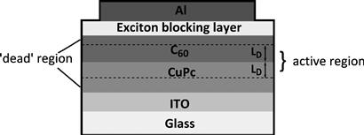
FIGURE 5 Architecture of a bilayer solar cell using copper phthalocyanine (CuPc) as the electron donor and buckminsterfullerene (C60) as the electron acceptor. The dashed lines demarcate the active region of the cell. Excitons generated outside this region will decay before reaching the donor–acceptor interface.
Bilayer efficiencies have reached around 5%, with the best devices using C60 as an electron acceptor and a phthalocyanine (typically, copper phthalocyanine CuPc) as the electron donor. Recent encouraging results have been achieved using pentacene [29] or subphthalocyanine [30] as the electron donor or by using long-wavelength absorbers such as tin or lead phthalocyanine, either alone or in ternary systems containing two light-absorbing components [31–32].
Bilayer solar cells present a major drawback: the charge separation efficiency is limited by the small interfacial area, a consequence of the limited diffusion length of the exciton in organic materials [6,33–34], which requires that a photogenerated exciton must be formed close to a donor–acceptor interface to have a chance of separating before it decays to its ground state. This limits the thickness of the exciton-generating layer in a bilayer device and hence prevents the use of thick films with greater light absorption. In general, the better-performing bilayer structures are based on small molecules rather than polymers, possibly because the greater crystalline order in these materials offers improved exciton diffusion. The bilayer concept has been further improved in vacuum-deposited cells by including a mixed donor–acceptor layer with the aim of increasing the available interfacial area for charge dissociation and approaching the morphology shown in [35]. The intermixing of donor and acceptor is the basis of the bulk heterojunction, which is described next.
3.3 Bulk Heterojunction Architecture
In order to overcome the limitation on device thickness due to the small exciton diffusion lengths in organic materials, the bulk heterojunction concept has been widely adopted. The basis of the bulk heterojunction is the intimate mixing of the donor and acceptor in a single layer, resulting in a film with a high interfacial surface area (Figure 6). Various types of bulk heterojunction system have been demonstrated, including polymer–fullerene blends (the main focus of this section), polymer–polymer blends, block copolymers, and inorganic–organic hybrid layers.
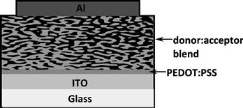
FIGURE 6 Bulk heterojunction blend. To maximize exciton dissociation, the domain sizes should be comparable to the exciton diffusion length.
The high interfacial surface area and the smaller donor and acceptor domains in a bulk heterojunction compared to a bilayer ensure that excitons are produced close enough to an interface that they may reach it before decaying. This greatly increases the probability of exciton dissociation and allows the use of thicker films with increased harvesting of light. However, the intermixing of the two phases into small domains tends to decrease the order in the molecular packing and means that continuous pathways are harder to produce, and isolated domains, which cause recombination losses, may exist. In addition, the larger interfacial area encourages recombination, and poor control of the phase morphology means that shunt pathways may exist. Balancing the increased photogeneration yield against the increased recombination losses requires the optimisation of the microstructure of the blend film (Section 4).
4 Optimising Solar Cell Performance
High power-conversion efficiency requires the efficient harvesting of visible light, the efficient conversion of photogenerated potential energy into photovoltage at the electrodes, and a high fill factor (which represents good photocurrent generation in forward bias). The total power-conversion efficiency η of a solar cell can be expressed as a product of three key parameters: (1) the short-circuit current Jsc, (2) the open-circuit voltage Voc, and (3) the fill factor FF (Equation (2), where Ps is the radiant power incident on the cell):
![]() (2)
(2)
The short-circuit current density Jsc measures the number of charges exiting the cell per unit time and area, and it has been shown to correlate strongly with the yield of photogenerated charges, provided the charge mobility is above around 10−5 cm2 V−1 s−1[36]. As such, for most organic semiconductors of interest for photovoltaics, the main parameters affecting Jsc are the light harvesting by the cell, a function of the absorption profile of the materials, absorption profile of the materials, the film thickness and optical confinement effects, the blend microstructure, and the efficiency of charge generation at the donor–acceptor heterojunction. The photovoltage is mainly determined by the offset of the energy levels at the donor–acceptor heterojunction and by bimolecular recombination. Bimolecular recombination also influences the fill factor, which is further determined by the parasitic resistances in the device (series resistance and shunt pathways). Bimolecular recombination in organic solar cells is strongly dependent upon charge-carrier density and energetic disorder (necessitating a model of device operation distinct from that of inorganic solar cells [37]) and the blend morphology.
4.1 Optimising Light Harvesting
Although organic semiconductors frequently have high absorption coefficients (~105 cm−1), their absorption tends to occur in fairly narrow bands (Figure 7). The available photon flux provided by the sun peaks at around 600 nm and contains large numbers of photons in the red or infrared. Polymers or acceptors with absorption in this long-wavelength region are desirable for increased light harvesting.
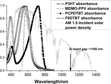
FIGURE 7 The absorption spectra of conjugated polymers are typically narrow and may not overlap well with the available solar emission spectrum. By comparison, Si has a band gap corresponding to an absorption edge at 1100 nm.
Materials with increased absorption at long wavelengths are desirable for OPV applications and are mostly based upon low-band-gap polymers [38] (many containing some charge-transfer character), although phthalocyanine or subphthalocyanine dyes [39], or inorganic nanoparticles [40], have also been employed to enhance light harvesting at longer wavelengths in dye-sensitised and hybrid organic-inorganic solar cells. Decreasing the material band gap to increase the number of photons absorbed has one disadvantage: this may also decrease the driving force for charge separation and lead to a decrease in the yield of photogenerated charges.
4.2 Optical Trapping
Because the layer thicknesses employed in organic solar cells are comparable to the wavelength of light, interference effects are important, and these can be manipulated to enhance optical absorption in the active layer. Light trapping can be achieved by the use of grating structures [41], microlenses [42–43], and pattern metal electrodes to induce plasmonic effects [44].
4.3 Optimising Voltage Generation
The photovoltage generated in a donor–acceptor OPV device is dependent upon the alignment of the energy levels of the donor and acceptor in the cell and also upon the rate of bimolecular recombination, which is discussed in the next section. One strategy to increase Voc is to increase the energy level offset at the interface by either lowering the donor HOMO or raising the acceptor LUMO. Theoretical studies have suggested that modifying the device energy levels in this way could result in device efficiencies of 10% or more [45]. Maintaining good device performance does, however, depend upon the effect of these changes upon the charge-generation efficiency (and hence the short-circuit current). Increasing the donor ionisation potential (Figure 8) increases the voltage but may reduce Jsc, either by increasing photon energy required to excite the molecule or by reducing the driving force for charge separation. In polymer–fullerene cells, an alternative is to reduce the electron affinity of the fullerene. The use of multiply substituted fullerenes leads to an increase in open-circuit voltage with no loss of charge generation in poly-3-hexylthiophene (P3HT) blends [46–47] but may adversely affect the blend morphology and reduce carrier mobility [48].
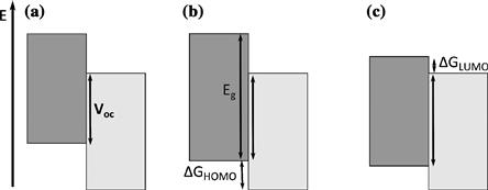
FIGURE 8 Increasing the open-circuit voltage (a) by increasing the polymer ionisation potential (b) results in an increased polymer band gap and decreased driving force for hole transfer, both of which may reduce short-circuit current. Maintaining the same band gap (c) results in a decreased driving force for electron transfer, with the same effect.
In some polyfluorene–fullerene blends, increasing the frontier orbital offset between the donor HOMO and the acceptor LUMO may also lead to the formation of triplet states that are detrimental to device performance [49–51] and are of concern for the long-term stability of devices (Section 5).
4.4 Optimising Electrodes for Voltage Generation
In order to extract the electrochemical potential generated by the absorbed light, the interface between the electrodes and the active layer must be optimised to provide an ohmic contact. Since the Fermi levels of organic materials are seldom easily altered by doping, achieving good contact to the active layer requires careful selection of the electrode materials. In a P3HT–PCBM device, the transport level for holes (the polymer HOMO) is 4.8 eV and for electrons (the PCBM LUMO) is around 4 eV (estimates range from 4.3 eV to 3.7 eV) below the vacuum level. In a ‘normal’ device configuration (Figure 6), this requires the use of a low-work-function metal as the cathode. This electrode is typically based on aluminium, although its work function of 4.3 eV typically requires the insertion of a thin layer of a lower-work-function material such as LiF or barium or calcium metal in order to extract electrons more efficiently [52]. The anode is normally based on indium-doped tin oxide (ITO), which has a work function of around 4.7 eV and is normally coated with a conducting layer of polyethylenedioxythiophene–poly(4-styrenesulfonate) (PEDOT–PSS), which increases the work function to 5.0 eV. While the electrode materials listed above are considered to be optimal for P3HT–PCBM blends, we are likely to need higher-work-function anodes or lower-work-function cathodes to contact to the new low-band-gap active materials discussed previously.
4.5 Organic Tandem Solar Cells
As discussed earlier, decreasing the band gap of the light-absorbing component increases the number of photons and leads to improved photocurrent generation. However, the excess energy in photons with energy greater than the band gap will be lost to thermalisation, reducing the attainable photovoltage. In order to avoid this, it is possible to use low-band-gap semiconductors in combination with higher-band-gap semiconductors in a tandem structure to achieve a higher voltage. The tandem architecture is shown in Figure 9 and requires the semiconductor materials to be deposited sequentially in layers. At first, this was a challenge for OPV because of the difficulty in processing several layers from solution without damaging the layers below, although much recent progress has been made, and all-solution processed tandem solar cells are now possible [23,53–54]. The intermediate layer in an organic tandem cell may be made of a metal such as gold or metal oxide [55] or based on the conducting polymer PEDOT–PSS [23,56]; its role is to provide a recombination region for charges and to ensure the alignment of the quasi-Fermi levels of electrons and holes in the two (or more) devices so that the photovoltages generated by the separate cells add. As usual, the photocurrent generated by the top and bottom cells should be equal.
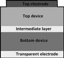
FIGURE 9 Tandem organic solar cell device architecture.
A detailed review of tandem organic solar cells is given in [57].
4.6 Optimising Microstructure of Bulk Heterojunctions
The structure of organic blends, both on the microscopic length scale and the exact structure of the interface, is extremely important in determining the charge-generation efficiency and fill factor in organic solar cells, but it has proved challenging to control. The degree of intermixing between materials depends upon many factors, including the blend ratio, the surface energies of the blend components (influencing the relative affinity of each material for the substrate, the air, and each other), and the device processing conditions. This section presents a summary of ways in which the morphology can be influenced and some strategies to improve performance.
4.7 Blend Composition
The blend composition is known to have a large effect: in blends of MDMO-PPV with PCBM, the optimum device performance is achieved using a blend containing 80% PCBM by weight [58–59]. This result, while initially unexpected on the basis that the majority of the light absorption occurs in the polymer, is explained by the surprising observation that increased PCBM content in the film actually increases the hole mobility [59–60]. Moreover, the formation of large PCBM domains is also thought to provide an improvement to charge photogeneration. In a study of polyfluorene–fullerene blend films[19], the increased charge separation efficiency in blends with larger PCBM domains was ascribed to an increase in the dielectric constant and local electron mobility, as the crystalline domains increased in size. Influence over domain sizes can be achieved by changes to the solvent- and spin-coating conditions [58,61–62] or by the use of blend additives [63–65] to increase control over the blend microstructure.
A great deal of research has been carried out into blends of P3HT with PCBM, and this system has until quite recently been held as a benchmark blend due to the possibility of achieving power-conversion efficiencies of more than 5%. P3HT–PCBM also provides an important demonstration of the ways in which the microstructure not only strongly influences the blend’s optoelectronic properties and ultimately device performance but also may be controlled. In P3HT–PCBM blends, the optimum blend composition requires 40–50% PCBM by weight, a much lower amount than is required for MDMO-PPV. In this system, the polymer crystallinity is high, and the formation of P3HT crystalline domains serves to expel the fullerene and decrease the level of intermixing between the materials. This results in less trapping of the fullerene in the polymer phase, and high fullerene content is not then required to produce a percolating network for electrons. The crystalline P3HT also has a reasonably high hole mobility and allows balanced charge transport. A study of the phase behaviour in P3HT–PCBM blends concluded that the composition required for optimum device performance is slightly below the eutectic point of the mixture, resulting in a blend with high interfacial area and optimal charge transport properties [66]. This was correlated both with photoluminescence quenching and the yield of photogenerated charges in a subsequent study [67].
4.8 Annealing
Post-treatment processing by annealing, either by heating above the glass transition temperature of the polymer or by placing in a solvent atmosphere, is known to be a necessary step to achieve the optimum performance in P3HT–PCBM blends [68–71]. Annealing results in an increased ordering in the blend as a result of crystallisation of the polymer, which is followed by clustering of the fullerene molecules. This results in improved charge-transport properties and charge-generation yield in the film [68], as well as an increase in the red-light absorption by the polymer. Vertical phase segregation has been observed upon annealing, which improves charge collection at the electrodes [72–73]. Annealing also has the effect of causing a decrease in the polymer ionisation potential (as a result of increased polymer crystallinity and the resulting increase in delocalisation of the HOMO) [68]. Increased crystallinity may also promote charge separation by an increase in the spatial extent of the exciton or in the local charge-carrier mobility, thus improving charge photogeneration yield [19].
4.9 Blend Additives
In recent years, a selection of molecular additives have been used in an attempt to optimise the morphology of polymer blends, particularly in systems where, unlike P3HT, the morphology cannot be so strongly influenced by annealing as a result of the lower crystallinity of the polymer. High performances have been achieved in polymer–PCBM [74–75] and small-molecule–PCBM [76] blends by the addition of 1,8-octanedithiol to the blend solution. The dithiol additive is believed to increase the phase segregation in the blend and provide better percolation pathways for electrons [77]. In blends of the polymer PCDTBT with the fullerene PC70BM, the addition of diiodooctane to the blend has been shown to reduce the yield of triplet formation, thereby improving the charge-generation yield in the film [63].
4.10 Alternative Approaches
Inorganic–organic hybrid devices offer another route to control of the active-layer morphology. In these devices, the electron acceptor is based upon a nanostructured metal oxide film, similar to the microporous metal oxides commonly employed in dye-sensitised solar cells. Devices utilising nanostructured metal oxide layers have achieved efficiencies of a few percent, with a range of structures including nanowires, nanorods, and ordered nanocrystals being formed by these materials [78–80].
Block copolymers are another way to manipulate the blend morphology and may offer an advantage over binary blends of better long-term stability in morphology. Block copolymers consist of two or more different polymer ‘blocks’ joined end to end, allowing two materials that would ordinarily be immiscible to be forced into close contact and giving rise to unique phase behaviour and well-defined morphologies [81]. They can be used either as a sacrificial template for photoactive materials (for example, to produce nanostructured oxide films, which may be filled by a conjugated polymer [82] or used in dye-sensitised solar cells [83]) or in the case of a conjugated block copolymer, as a single active-layer component [84–85]. Block copolymers have been shown to improve the long-term stability of morphology in P3HT–PCBM blends when used as a compatibilising agent, decreasing the tendency of the blend to phase segregate over time [86]. In the long term, block copolymers are promising candidates in that the length scale of phase segregation is ‘written in’ to the material during synthesis, and so the solar cell performance should be less sensitive to variations in processing.
5 Production Issues
The previous sections have dealt with the research challenges involved in increasing power-conversion efficiencies in organic solar cells, mainly at the laboratory scale. Now we address some of the key issues facing the production of these devices for commercial applications.
5.1 Substrates
In order to realise the potential of organic solar cells in unique applications and their mass production by roll-to-roll processes, flexible substrates are required. The most widely used material is ITO-coated poly(ethylene terephthalate) (PET).
At present, the transparent conductor used as the basis for OPV is indium-doped tin oxide. This material is limited by its transmission of visible light (80–90), high resistivity (typically 10–100 Ohm-cm2) and susceptibility to mechanical stress, a problem for the production of flexible devices. Indium is also a limited and expensive resource, limiting the cost reductions available by using organic semiconductors in solar cells. As a result, alternatives to ITO are being sought. These include the alternative oxide material fluorine-doped tin oxide (FTO), which is cheaper but cannot be deposited on plastic substrates. Organic conducting coatings—for example, high-conductivity PEDOT–PSS or vapour-phase–polymerised PEDOT (VPP-PEDOT)—single-walled carbon nanotubes [87] and metal electrodes in an inverted geometry [88] have also been demonstrated as ITO alternatives in OPV devices.
5.2 Stability
One of the major challenges facing the field of organic photovoltaics is the limited stability of devices. Although impressive recent stability results have been achieved in accelerated degradation tests, organic solar cells do not yet achieve lifetimes of more than a few thousand hours (equivalent to a few years insolation in northern latitudes [89]), limiting their scope to small-scale consumer products rather than large-scale building-integrated applications. There are many sources of degradation for organic solar cells, mostly caused by the ingress of water and oxygen to the cell or by reactions at the electrodes. A detailed review of solar cell degradation processes and the measurement techniques used to characterise them is given in [90].
5.3 Degradation of Materials
Organic materials are susceptible to photodegradation, particularly when in contact with water or oxygen. Oxygen doping of conjugated polymers is well known, and the formation of triplet states upon photoexcitation offers another degradation pathway through the resulting reactivity to the triplet ground state of atmospheric oxygen. The chemical degradation of the materials depends on their molecular structure; the presence of reactive groups either within the polymer repeat units (such as the vinyl linkages in PPV-type polymers) or at the ends of the polymer chain. The development of materials with decreased reactivity is central to solving this problem [91].
5.4 Degradation of Morphology
In many types of bulk heterojunction solar cell, the morphology for optimal device performance is a nonequilibrium structure (it is ‘frozen in’ by the fast drying of the solvent during deposition). Over time, the structure may evolve toward a more stable molecular arrangement with an accompanying decrease in device performance. Most strategies to prevent this are based on materials designed to produce a thermodynamically stable morphology in the first place, although other approaches including the use of cross-linkable polymers have been shown to reduce the degradation in device performance over time [92].
5.5 Degradation of Electrodes
The electrodes and the electrode-active layer interfaces are another source of instability. Metal electrodes, particularly the low-work-function metals used for devices in a standard configuration, may react with atmospheric oxygen. Using an inverted device architecture (Figure 10) allows higher-work-function metals to be used or even conducting polymer anodes that can be used with printed silver ink cathodes, avoiding the need for metal evaporation and resulting in fully solution-processible devices [93]. Inverted devices also require an additional layer, frequently TiO2, at the cathode. Although inverted-device performances are so far limited to less than 5% [94], they are gaining interest for their relative ease of manufacture. ITO may undergo chemical degradation, causing indium atoms to leach into the active layer, and it has limited mechanical strength cracking when flexed. The PEDOT–PSS layer is also susceptible to the rapid uptake of water and migration of PSS ions over time. Alternatives to PEDOT–PSS include metal oxides such as MoO3, V2O5 [95], and NiO [96] and solution-processible graphene oxide [97].
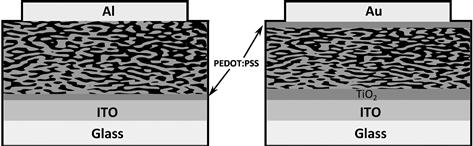
FIGURE 10 Normal (left) and inverted (right) devices.
5.6 Encapsulation
At the laboratory scale, the fabrication of devices is frequently carried out in an inert environment to avoid the atmospheric degradation of the organic materials. However, at a manufacturing plant level, maintaining oxygen-free environments would result in a significant cost increase for the product. Encapsulation will be essential in prolonging the shelf life of commercially produced OPV devices and is already routine in the production of organic light-emitting diodes (OLEDs) [98].
The main requirement for encapsulating materials is that they should have low permeability to oxygen and water. Glass is a reliable material for encapsulation, leading to lifetimes of several thousand hours, but it negates the key advantage of organic solar cells, their flexibility, and the resulting low production cost. Flexible devices require encapsulation to be performed by applying a flexible plastic layer with barrier layers applied to reduce the permeability to ambient degrading agents. This approach has been demonstrated using, for example, poly(ethylene naphthalate) films coated with alternating layers of silicon oxide and organosilicon compounds that improve the lifetime of MDMO-PPV–PCBM and P3HT–PCBM cells to more than 3000 hours and 6000 hours, respectively [99–100].
5.7 Deposition Processes
Most photovoltaic devices produced at the laboratory scale are prepared by spin coating, but this technique is not amenable to scaling up to production levels. Large-scale device manufacture will require scalable and high-throughput production techniques, which for flexible substrates can be performed in a roll-to-roll manner.
A range of printing and deposition techniques have been shown to be effective in preparing organic solar cells, including printing techniques such as screen printing [101], ink-jet printing [102], slot-die coating [103–104], and gravure printing [105–106], deposition in vacuo or spray coating [107–109]. An overview of some of the different processes is given in Figure 11.
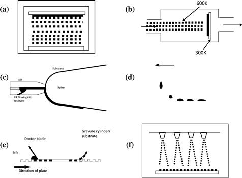
FIGURE 11 Deposition processes amenable to solar cell production: (a) thermal evaporation, (b) organic molecular beam deposition, (c) slot-die coating, (d) ink-jet printing, (e) gravure printing, (f) spray coating.
6 Conclusions
Organic solar cells have moved from low-efficiency laboratory-scale devices to the first commercial products in less than a decade. The highest efficiencies are still mostly achieved using bulk heterojunction devices made from conjugated polymers and fullerene acceptors, although other classes of organic solar cell are beginning to compete. The main challenges for future development of the technology are to continue the improvements to device efficiency by materials design to achieve high light harvesting, high photovoltage, control of blend microstructure, the development of new electrodes to compete with and ultimately supplant the ubiquitous yet expensive ITO, and improvement to the long-term stability of devices. Roll-to-roll printing and coating processes employing flexible substrates are highly compatible with organic solar cells with the main challenges for production being in morphology control and in increasing device stability through a combination of materials design and device encapsulation.
References
1. Spanggaard H, Krebs FC. A brief history of the development of organic and polymeric photovoltaics. Sol Energy Mater Sol Cells. 2004;83(2–3):125–146.
2. Volmer M. Die verschiedenen lichtelektrischen Erscheinungen am Anthracen, ihre Beziehungen zueinander, zur Fluoreszenz und Dianthracenbildung. Annalen der Physik. 1913;345(4):775–796.
3. Konarka. Konarka’s power plastic achieves world record 8.3% efficiency certification from national energy renewable laboratory (NREL). 2010 Nov. 29, 2010 [cited 2011 22 February]; Press release]. Available from: http://www.konarka.com/index.php/site/pressreleasedetail/konarkas_power_plastic_achieves_world_record_83_efficiency_certification_fr/.
4. Heliatek, Heliatek and IAPP achieve production-relevant efficiency record for organic photovoltaic cells. 11 November 2010.
5. Konarka. http://www.konarka.com/index.php/power-plastic/about-power-plastic/. 2011 [cited 2011 10 March].
6. Mikhnenko OV, et al. Temperature dependence of exciton diffusion in conjugated polymers. J Phys Chem B. 2008;112(37):11601–11604.
7. Ohkita H, et al. Charge carrier formation in polythiophene/fullerene blend films studied by transient absorption spectroscopy. J Am Chem Soc. 2008;130(10):3030–3042.
8. Halls JJM, et al. Charge and energy transfer processes at polymer/polymer interfaces: A joint experimental and theoretical study. Phys Rev B. 1999;60(8):5721–5727.
9. Deibel C, Strobel T, Dyakonov V. Role of the charge transfer state in organic donor-acceptor solar cells. Adv Mater. 2010;.
10. Lee J, et al. Charge transfer state versus hot exciton dissociation in polymer-fullerene blended solar cells. J Am Chem Soc. 2010;132(34):11878–11880.
11. Hallermann M, Haneder S, Da Como E. Charge-transfer states in conjugated polymer/fullerene blends: below-gap weakly bound excitons for polymer photovoltaics. Appl Phys Lett. 2008; 05330793 (2008) 053307.
12. Veldman D, Meskers SCJ, Janssen RAJ. The energy of charge-transfer states in electron donor-acceptor blends: insight into the energy losses in organic solar cells. Adv Funct Mater. 2009;19(12):1939–1948.
13. Pal SK, et al. Geminate charge recombination in polymer/fullerene bulk heterojunction films and implications for solar cell function. J Am Chem Soc. 2010;132(35):12440–12451.
14. Benson-Smith J, et al. Formation of a ground-state charge-transfer complex in polyfluorene/[6,6]-phenyl-C61 butyric acid methyl ester (PCBM) blend films and its role in the function of polymer/PCBM solar cells. Adv Funct Mater. 2007;17(3):451–457.
15. Goris L, et al. Observation of the subgap optical absorption in polymer-fullerene blend solar cells. Appl Phys Lett. 2006;88(5):052113.
16. Vandewal K, et al. The relation between open-circuit voltage and the onset of photocurrent generation by charge-transfer absorption in polymer: Fullerene bulk heterojunction solar cells. Adv Funct Mater. 2008;18(14):2064–2070.
17. Yin C, et al. Relation between exciplex formation and photvoltaic properties of PPV polymer-based blends. Sol Energy Mater Sol Cells. 2007;91:411–415.
18. Keivanidis PE, et al. Delayed luminescence spectroscopy of organic photovoltaic binary blend films: probing the emissive non-geminate charge recombination. Adv Mater. 2010;22(45):5183–5187.
19. Veldman D, et al. Compositional and electric field dependence of the dissociation of charge transfer excitons in alternating polyfluorene copolymer/fullerene blends. J Am Chem Soc. 2008;130:7721–7735.
20. Westenhoff S, et al. Charge recombination in organic photovoltaic devices with high open-circuit voltages. J Am Chem Soc. 2008;130(41):13653–13658.
21. Pensack RD, Asbury JB. Barrierless free carrier formation in an organic photovoltaic material measured with ultrafast vibrational spectroscopy. J Am Chem Soc. 2009;131(44):15986–15987.
22. Forrest SR. Ultrathin organic films grown by organic molecular beam deposition and related techniques. Chem Rev. 1997;97(6):1793–1896.
23. Gilot J, Wienk MM, Janssen RAJ. Double and triple junction polymer solar cells processed from solution. Appl Phys Lett. 2007;90(14):143512–143513.
24. O’Brien D, et al. Use of poly(phenyl quinoxaline) as an electron transport material in polymer light-emitting diodes. Appl Phys Lett. 1996;69(7):881–883.
25. Wiedemann W, et al. Nanostructured interfaces in polymer solar cells. Appl Phys Lett. 2010;96(26):263109–263113.
26. Kim JB, et al. Reversible soft-contact lamination and delamination for non-invasive fabrication and characterization of bulk-heterojunction and bilayer organic solar cells. Chem Mater. 2010;22(17):4931–4938.
27. Granstrom M, et al. Laminated fabrication of polymeric photovoltaic diodes. Nature. 1998;395(6699):257–260.
28. Ferenczi TAM, et al. Planar heterojunction organic photovoltaic diodes via a novel stamp transfer process. J Phys.: Condens Matter. 2008;20(47):475203.
29. Yoo S, Domercq B, Kippelen B. Efficient thin-film organic solar cells based on pentacene/C[sub 60] heterojunctions. Appl Phys Lett. 2004;85(22):5427–5429.
30. Gommans HHP, et al. Electro-optical study of subphthalocyanine in a bilayer organic solar cell. Adv Funct Mater. 2007;17(15):2653–2658.
31. Dai J, et al. Organic photovoltaic cells with near infrared absorption spectrum. Appl Phys Lett. 2007;91(25):253503–253513.
32. Rand BP, et al. Organic solar cells with sensitivity extending into the near infrared. Appl Phys Lett. 2005;87(23):233508–233513.
33. Scully SR, McGehee MD. Effects of optical interference and energy transfer on exciton diffusion length measurements in organic semiconductors. J Appl Phys. 2006;100:3.
34. Athanasopoulos S, et al. Trap limited exciton transport in conjugated polymers. J Phys Chem C. 2008;112(30):11532–11538.
35. Xue J, et al. A hybrid planar-mixed molecular heterojunction solar cell, Adv. Mater. 2005;17(1):66–71.
36. Clarke TM, et al. Analysis of charge photogeneration as a key determinant of photocurrent density in polymer: fullerene solar cells. Adv Mater. 2010;22(46):5287–5291.
37. Shuttle CG, et al. Charge-density-based analysis of the current–voltage response of polythiophene/fullerene photovoltaic devices. Proc Natl Acad Sci U.S.A. 2010;107(38):16448–16452.
38. Winder C, Sariciftci NS. Low bandgap polymers for photon harvesting in bulk heterojunction solar cells. J Mater Chem. 2004;1077–1086 1077–108614 (2004).
39. Cid J-J, et al. Molecular cosensitization for efficient panchromatic dye-sensitized solar cells. Angew Chem Int Ed. 2007;46(44):8358–8362.
40. Chang JA, et al. High-performance nanostructured inorganic–organic heterojunction solar cells. Nano Lett. 2010;10(7):2609–2612.
41. Niggemann M, et al. Diffraction gratings and buried nano-electrodes–architectures for organic solar cells. Thin Solid Films 451–452 2004;619–623.
42. S.D. Zilio, et al., Fabrication of a light trapping system for organic solar cells, Microelectronic Eng. 86(4–6) 1150–1154.
43. Tvingstedt K, et al. Trapping light with micro lenses in thin film organic photovoltaic cells. Opt Express. 2008;16(26):21608–21615.
44. Reilly TH, et al. Surface-plasmon enhanced transparent electrodes in organic photovoltaics. Appl Phys Lett. 2008;92(24):243304–243313.
45. Scharber MC, et al. Design rules for donors in bulk-heterojunction solar cells— towards 10% energy-conversion efficiency. Adv Mater. 2006;18(6):789–794.
46. Faist MA, et al. Effect of multiple adduct fullerenes on charge generation and transport in photovoltaic blends with poly(3-hexylthiophene-2,5-diyl). J Polym Sci Part B: Pol Phys. 2010;49(1):45–51.
47. Lenes M, et al. Fullerene bisadducts for enhanced open-circuit voltages and efficiencies in polymer solar cells. Adv Mater. 2008;20(11):2116–2119.
48. Lenes M, et al. Electron trapping in higher adduct fullerene-based solar cells. Adv Funct Mater. 2009;19(18):3002–3007.
49. Benson-Smith JJ, et al. Charge separation and fullerene triplet formation in blend films of polyfluorene polymers with [6,6]-phenyl C61 butyric acid methyl ester. Dalton Trans 2009 2009;10000–10005.
50. Cook S, et al. Singlet exciton transfer and fullerene triplet formation in polymer- fullerene blend films. Appl Phys Lett (2006) 10112889 2006;101128.
51. Dyer-Smith C, et al. Triplet formation in fullerene multi-adduct blends for organic solar cells and its influence on device performance. Adv Funct Mater. 2010;20(16):2701–2708.
52. Brabec CJ, et al. Effect of LiF/metal electrodes on the performance of plastic solar cells. Appl Phys Lett. 2002;80(7):1288–1290.
53. Kim JY, et al. Efficient tandem polymer solar cells fabricated by all-solution processing. Science. 2007;317(5835):222–225.
54. Hagemann O, et al. All solution processed tandem polymer solar cells based on thermocleavable materials. Sol Energy Mater Sol Cells. 2008;92(11):1327–1335.
55. Janssen AGF, et al. Highly efficient organic tandem solar cells using an improved connecting architecture. Appl Phys Lett. 2007;91(7):073519–073623.
56. Hadipour A, et al. Solution-processed organic tandem solar cells. Adv Funct Mater. 2006;16(14):1897–1903.
57. Ameri T, et al. Organic tandem solar cells: a review. Energy Environ Sci. 2009;2(4):347–363.
58. van Duren JKJ, et al. Relating the morphology of poly(p-phenylene vinylene)/methanofullerene blends to solar-cell performance. Adv Funct Mater. 2004;14(5):425–434.
59. Mihailetchi V, et al. Compositional dependence of the performance of poly(p-phenylene vinylene):methanofullerene bulk-heterojunction solar cells. Adv Funct Mater. 2005;15(5):795–801.
60. Tuladhar S, et al. Ambipolar charge transport in films of methanofullerene and poly(Phenylenevinylene)/methanofullerene blends. Adv Funct Mater (2005) 1171–118215 2005;1171–1182.
61. Moons E. Conjugated polymer blends: Linking film morphology to performance of light emitting diodes and photdiodes. J Phys.: Condens Matter. 2002;14:12235–12260.
62. DeLongchamp DM, et al. Variations in semiconducting polymer microstructure and hole mobility with spin-coating speed. Chem Mater (2005) 5610–561217 2005;5610–5612.
63. Nuzzo DD, et al. Improved film morphology reduces charge carrier recombination into the triplet excited state in a small bandgap polymer-fullerene photovoltaic cell. Adv Mater. 2010;22(38):4321–4324.
64. Moon JS, et al. Effect of processing additive on the nanomorphology of a bulk heterojunction material. Nano Lett. 2010;10(10):4005–4008.
65. Lee JK, et al. Processing additives for improved efficiency from bulk heterojunction solar cells. J Am Chem Soc. 2008;130(11):3619–3623.
66. Müller C, et al. Binary organic photovoltaic blends: a simple rationale for optimum compositions. Adv Mater. 2008;20:3510–3515.
67. P.E. Keivanidis, et al., Dependence of charge separation efficiency on film microstructure in poly(3-hexylthiophene-2,5-diyl): 6,6-phenyl-C-61 butyric acid methyl ester blend films. J. Phys. Chem. Lett. 1 (4) 734-738.
68. Clarke TM, et al. Free energy control of charge photogeneration in polythiophene/fullerene solar cells: the influence of thermal annealing on p3ht/pcbm blends. Adv Funct Mater. 2008;18(24):4029–4035.
69. Nguyen L, et al. Effects of annealing on the nanomorphology and performance of poly(alkylthiophene):fullerene bulk-heterojunction solar cells. Adv Funct Mater. 2007;17(7):1071–1078.
70. Reyes-Reyes M, Kim K, Carroll DL. High-efficiency photovoltaic devices based on annealed poly(3-hexylthiophene) and 1-(3-methoxycarbonyl)-propyl-1-phenyl- (6,6)C61 blends. Appl Phys Lett. 2005;87(8):083506.
71. Keivanidis PE, et al. Dependence of charge separation efficiency on film microstructure in poly(3-hexylthiophene-2,5-diyl):[6,6]-phenyl-C61 butyric acid methyl ester blend films. The J Phys Chem Lett. 2010;1(4):734–738.
72. Kim Y, et al. Device annealing effect in organic solar cells with blends of regioregular poly(3-hexylthiophene) and soluble fullerene. Appl Phys Lett. 2005;86:063502.
73. Campoy-Quiles M, et al. Morphology evolution via self-organization and lateral and vertical diffusion in polymer:fullerene solar cell blends. Nat Mater (2008) 158–1647 2008;158–164.
74. Coates NE, et al. 1,8-octanedithiol as a processing additive for bulk heterojunction materials: Enhanced photoconductive response. Appl Phys Lett. 2008;93(7):072105–072113.
75. Hwang I-W, et al. Carrier generation and transport in bulk heterojunction films processed with 1,8-octanedithiol as a processing additive. J Appl Phys. 2008;104(3):033706–033709.
76. Fan H, et al. Efficiency enhancement in small molecule bulk heterojunction organic solar cells via additive. Appl Phys Lett. 2010;97(13):133302–133303.
77. Morana M, et al. Bipolar charge transport in PCPDTBT-PCBM Bulk-heterojunctions for photovoltaic applications. Adv Funct Mater. 2008;18(12):1757–1766.
78. Ravijaran P, et al. Hybrid polymer/zinc oxide photovoltaic devices with vertically oriented ZnO nanorods and an amphiphilic molecular interface layer. J Phys Chem B. 2006;110:7635–7639.
79. Rattanavoravipa T, Sagawa T, Yoshikawa S. Photovoltaic performance of hybrid solar cell with TiO2 nanotubes arrays fabricated through liquid deposition using ZnO template, Sol. Energy Mater Sol Cells. 2008;92(11):1445–1449.
80. Bouclé J, et al. Hybrid solar cells from a blend of poly(3-hexylthiophene) and ligand-capped TiO2 nanorods. Adv Funct Mater. 2008;18(4):622–633.
81. Khandpur AK, et al. Polyisoprene-polystyrene diblock copolymer phase diagram near the order-disorder transition. Macromolecules. 1995;28(26):8796–8806.
82. Coakley KM, McGehee MD. Photovoltaic cells made from conjugated polymers infiltrated into mesoporous titania. Appl Phys Lett. 2003;83(16):3380–3382.
83. Crossland EJW, et al. Block copolymer morphologies in dye-sensitized solar cells: probing the photovoltaic structure–function relation. Nano Lett. 2008;9(8):2813–2819.
84. Bu L, et al. Monodisperse co-oligomer approach toward nanostructured films with alternating donor–acceptor lamellae. J Am Chem Soc. 2009;131(37):13242–13243.
85. Zhang Q, et al. Donor–acceptor poly(thiophene-block-perylene diimide) copolymers: synthesis and solar cell fabrication. Macromolecules. 2009;42(4):1079–1082.
86. Sivula K, et al. Amphiphilic diblock copolymer compatibilizers and their effect on the morphology and performance of polythiophene:fullerene solar cells. Adv Mater. 2006;18(2):206–210.
87. van de Lagemaat J, et al. Organic solar cells with carbon nanotubes replacing In[sub 2]O[sub 3]:Sn as the transparent electrode. Appl Phys Lett. 2006;88(23):233503–233513.
88. Zimmermann B, et al. ITO-free wrap through organic solar cells–A module concept for cost-efficient reel-to-reel production, Sol. Energy Mater Sol Cells. 2007;91(5):374–378.
89. Hauch JA, et al. Flexible organic P3HT: PCBM bulk-heterojunction modules with more than 1 year outdoor lifetime, Sol. Energy Mater Sol Cells. 2008;92(7):727–731.
90. Jørgensen M, Norrman K, Krebs FC. Stability/degradation of polymer solar cells, Sol. Energy Mater Sol Cells. 2008;92(7):686–714.
91. Hee Kim S, et al. Long-lived bulk heterojunction solar cells fabricated with photo-oxidation resistant polymer, Sol. Energy Mater Sol Cells. 2011;95(1):361–364.
92. Miyanishi S, Tajima K, Hashimoto K. Morphological stabilization of polymer photovoltaic cells by using cross-linkable poly(3-(5-hexenyl)thiophene). Macromolecules. 2009;42(5):1610–1618.
93. Krebs FC. All solution roll-to-roll processed polymer solar cells free from indium- tin-oxide and vacuum coating steps. Org Electron. 2009;10(5):761–768.
94. Hau SK, Yip H-L, Jen AK-Y. A review on the development of the inverted polymer solar cell architecture. Polym Rev. 2010;50(4):474–510.
95. Shrotriya V, et al. Transition metal oxides as the buffer layer for polymer photovoltaic cells. Appl Phys Lett. 2006;88(7):073508–073513.
96. Irwin MD, et al. p-Type semiconducting nickel oxide as an efficiency-enhancing anode interfacial layer in polymer bulk-heterojunction solar cells. Proc Natl Acad Sci U.S.A. 2008;105(8):2783–2787.
97. Li S-S, et al. Solution-processable graphene oxide as an efficient hole transport layer in polymer solar cells. ACS Nano. 2010;4(6):3169–3174.
98. Chwang AB, et al. Thin film encapsulated flexible organic electroluminescent displays. Appl Phys Lett. 2003;83(3):413–415.
99. Dennler G, et al. A new encapsulation solution for flexible organic solar cells. Thin Solid Films 511–512 2006;349–353.
100. Lungenschmied C, et al. Flexible, long-lived, large-area, organic solar cells, Sol. Energy Mater Sol Cells. 2007;91(5):379–384.
101. Shaheen SE, et al. Fabrication of bulk heterojunction plastic solar cells by screen printing. Appl Phys Lett. 2001;79(18):2996–2998.
102. Hoth CN, et al. Printing highly efficient organic solar cells. Nano Lett. 2008;8(9):2806–2813.
103. Alstrup J, et al. Ultra fast and parsimonious materials screening for polymer solar cells using differentially pumped slot-die coating. ACS Appl Mater Interfaces. 2010;2(10):2819–2827.
104. Y. Galagan, et al., Technology development for roll-to-roll production of organic photovoltaics. Chemical Engineering and Processing: Process Intensification. In Press, Corrected Proof.
105. Voigt MM, et al. Gravure printing for three subsequent solar cell layers of inverted structures on flexible substrates, Sol. Energy Mater Sol Cells. 2011;95(2):731–734.
106. Kopola P, et al. High efficient plastic solar cells fabricated with a high-throughput gravure printing method, Sol. Energy Mater Sol Cells. 2010;94(10):1673–1680.
107. Chen L-M, et al. Multi-source/component spray coating for polymer solar cells. ACS Nano. 2010;4(8):4744–4752.
108. Girotto C, et al. Exploring spray coating as a deposition technique for the fabrication of solution-processed solar cells, Sol. Energy Mater Sol Cells. 2009;93(4):454–458.
109. Vak D, et al. Fabrication of organic bulk heterojunction solar cells by a spray deposition method for low-cost power generation. Appl Phys Lett. 2007;91(8):081102–081103.