Chapter IC-6
High Efficiency III–V Multijunction Solar Cells
Chapter Outline
2. Special Aspects of III–V Multijunction Solar Cells
2.1. Fields of Application and Reference Conditions
2.3. Band Gap Versus Lattice Constant
2.6. Design of Concentrator Solar Cells
3.1. Lattice-Matched Triple-Junction Solar Cells on Ge
3.3. Upright Metamorphic Growth on Ge
3.4. Inverted Metamorphic Growth
1 Introduction
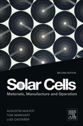
Solar cells made of III–V semiconductors reach the highest efficiencies of any photovoltaic technology so far. The materials used in such solar cells are composed of compounds of elements in groups III and V of the periodic table. Figure 1 shows the development of record efficiencies of III–V multijunction solar cells under concentrated sunlight over the last two decades. An impressive increase from about 32% in the early 1990s to more than 43% in 2011 has been achieved. The prerequisite for such high efficiencies is the ability to stack solar cells made of different III–V semiconductors. This enables an efficient use of the solar spectrum. Figure 2(a) shows a scheme of a typical triple-junction solar cell. Three subcells consisting of GaInP, GaInAs, and Ge are stacked on top of each other and are series interconnected by tunnel diodes. The key to efficient use of the solar spectrum is that each subcell has a higher band gap than the one below it. In this way, each subcell absorbs light from a spectral range closest to its band gap, hence reducing thermalisation losses (Figure 2(b)). Moreover, transmission losses can also be reduced if the lowest band gap of the stack has a lower band gap than do the conventional single-junction solar cells.

FIGURE 1 Development of best-realized efficiencies of III–V multijunction concentrator solar cells. Data are based on the Solar Cell Efficiency Tables, in which record efficiencies have regularly been published since 1993 [1]. The latest edition considered here is reference [2].
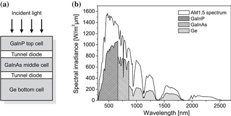
FIGURE 2 (a) Schematic structure of a monolithic GaInP–GaInAs–Ge triple-junction solar cell, which represents the state-of-the-art approach for III–V multijunction solar cells. (b) Spectral irradiance of the AM1.5 spectrum together with the parts of the spectrum that can be used by a triple-junction solar cell.
This approach results in a device with only one positive and one negative contact. As the subcells are connected in series within the multijunction solar cell, the total current is limited by the lowest current generated by one of the subcells. Therefore, current matching of the subcells is a central design aspect for III–V multijunction solar cells, which will be discussed in more detail in this chapter. In recent years, III–V multijunction solar cells have usually been grown by metal-organic vapour phase epitaxy (MOVPE) reactors, resulting in favourable economics of growth as well as high crystal quality. Large-area commercial MOVPE reactors are available from different companies.
III–V multijunction solar cells are used in different applications, the most prominent being satellites and space vehicles as well as terrestrial concentrator systems. Record efficiencies of 34.2% (AM0, 1367 W/m2) [3] and 43.5% (AM1.5d, 418 suns) [2] have already been realized in these fields. Intensive research is ongoing to further optimize the cell structures in order to achieve even higher efficiencies. Various approaches for III–V multijunction solar cells are currently investigated. This chapter summarizes the state of the art as well as recent trends of these devices. The first part describes special features of III–V multijunction solar cells in comparison to conventional single-junction solar cells. The second part discusses some of the different approaches and designs for III–V solar cells.
2 Special Aspects of III–V Multijunction Solar Cells
III–V multijunction solar cells differ from conventional single-junction solar cells in several aspects. This section introduces these features.
2.1 Fields of Application and Reference Conditions
III–V multijunction solar cells are used in different applications. They have become the state-of-the-art photovoltaic power generator for satellites and space vehicles [4]. This development was driven by the fact that III–V multijunction solar cells are particularly suitable for specific needs in space. They offer high reliability, a high power-to-mass ratio, excellent radiation hardness, small temperature coefficients, and the possibility to operate at high voltage and low current [5]. Despite their higher production costs compared to silicon solar cells, III–V multijunction solar cells are integrated into flat-plate modules for space applications. This becomes feasible as the determining measure for cost in space applications are €/kg rather than €/Wp as in terrestrial applications. The different measure originates from the consideration of launch costs as well as of spacecraft attitude control [6]. Due to their higher power-to-mass ratio (W/kg), flat-plate modules of III–V multijunction solar cells are beneficial under these cost considerations.
The use of III–V multijunction solar cells in flat-plate modules on Earth would currently be too expensive. However, the expensive cell area can be reduced by using a cost-efficient concentrating optic. In recent years, many companies have implemented this idea by placing III–V multijunction solar cells into terrestrial concentrator systems. Most of these systems use high concentration factors above 400, which enables a significant cost reduction and also leads to higher efficiencies. An extensive overview about CPV can be found in reference [7]. For a recent review on the status and forecast of CPV efficiencies, see reference [8].
In addition to their use in space and terrestrial concentrator systems, III–V solar cells are also used in several niche applications. One of these is thermophotovoltaics (TPV). In such systems, light from an emitter other than the sun is converted to electricity by photovoltaic cells. The emitter can either be a flame or a material that is heated to a temperature between 1000 °C and 1500 °C [9] by the sun or by burning fuel. As the emitted spectrum is shifted toward longer wavelengths compared to the spectrum of the sun, TPV photovoltaic cells need to have a rather small band gap. Materials like Ge, GaSb, and InGaAs(Sb) are suitable. TPV could, for example, enable the use of industrial waste heat for electricity generation and offer advantages like high-power density outputs, in-phase supply and demand, and potential low cost [10]. A detailed overview about TPV can be found in references [11,12].
III–V photovoltaic cells are also used as laser power converters, which convert light emitted by a laser into electricity [13–18]. This is a promising alternative to using copper wires as source and load can be electrically isolated giving improved safety, e.g., in explosive areas as well as reducing the influence of electromagnetic pulses and interferences. Possible applications of these power-by-light systems are sensor applications in industrial monitoring as well as medical diagnostic tools [18]. Recently, an optically powered camera video link was realized, which proves that complex information can be transmitted in such a system [19].
Depending on the intended field of application III–V multijunction solar cells are rated with different reference spectra. For space applications the reference spectrum AM0 (with a total irradiance of 1367 W/m2) is used [20]. For terrestrial concentrator applications the AM1.5d spectrum (1000 W/m2) is applicable, which only takes direct irradiance into account. Due to the concentration of the incident light a concentration ratio needs to be indicated for measurements under AM1.5d. The unit of this factor is ‘suns’ with ‘1 sun’ corresponding to unconcentrated incident light. For solar cells in conventional flat-plate modules on Earth the global AM1.5 g spectrum is applicable. Both terrestrial reference spectra are currently defined in the norm ASTM G173 03 [21].
2.2 Band-Gap Choice
One of the benefits of using III–V semiconductors for multijunction solar cells is the wide flexibility in band-gap combinations that can be realized. Thus, the first decision to be made when designing a III–V multijunction solar cell is the number of junctions and band-gap combinations to be chosen. Ignoring possible restrictions due to other material properties such as lattice constant, achievable material quality and availability, the question of choosing the optimal band-gap combinations comes down to optimizing in which parts the solar spectrum should be divided by the multijunction solar cell (see Figure 2). This determines on one hand the current densities of the subcells and on the other hand their voltages.
Different models are used for this optimisation (for an overview see Kurtz et al. [22]). One widely used method is the ‘detailed balance approach’ suggested by Shockley and Queisser [23], which allows us to calculate the theoretical conversion efficiency of a solar cell with a given band-gap energy under a defined spectrum. Only radiative recombination is considered because this is the only unavoidable recombination mechanism. In addition, ideal solar cells are assumed that have an external quantum efficiency of unity and behave according to the one-diode model. As a rule of thumb, between 70% and 80% of the theoretical efficiencies can be achieved in reality. This approach was, for example, implemented for single and multijunction solar cells in the program etaOpt [24], which is also available for download on the Website of Fraunhofer ISE. Figure 3 shows the maximum efficiencies (AM1.5d, 500) suns calculated with etaOpt for different numbers of p–n junctions. The numbers in the bars indicate the optimal band-gap combination. The efficiency increases with the number of subcells. However, the gain of efficiency for any additional junction gets smaller with increasing number of junctions.
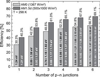
FIGURE 3 Theoretical efficiency limit versus number of p–n junctions under the reference spectrum AM0 (1367 W/m2) for space applications [20] as well as under the reference spectrum AM1.5d (500×1000 W/m2) for concentrator solar cells [21]. The calculation was carried out with the program etaOpt [24], which implements the detailed balance approach of Shockley and Queisser [23].
In recent years a trend toward evaluating the potential of different band-gap combinations and solar cell concepts for terrestrial concentrator applications in terms of energy yield is observable, e.g., [25–29]. This is motivated by the fact that the main value of interest in real applications is not the efficiency under a reference spectrum but the annual energy production under realistic operating conditions. Since multijunction solar cells are known to be sensitive to changes in the solar spectrum, e.g., [25,30–34], spectral variation throughout day and year should be taken into account when calculating the annual energy production of these solar cells. Owing to this aspect the potential of several solar cell concepts discussed in this chapter is evaluated with the energy-harvesting efficiency which is the total energy produced by a cell in a year divided by the incident solar energy at the investigated location [26].
2.3 Band Gap Versus Lattice Constant
Realizing III–V multijunction solar cells with an optimal band-gap combination can be a challenging task. To understand the problems it is important to note that each (III–V) semiconductor is characterized by a band gap as well as a characteristic lattice constant. Figure 4 shows the relation between band gap and lattice constant for various semiconductors which are important for III–V solar cells. The band-gap combination of the most common Ga0.50In0.50P–Ga0.99In0.01As–Ge triple-junction solar cell (Figure 9) is indicated as an example. As all materials in this structure nearly have the same lattice constant, the approach is called lattice matched. In contrast to this devices with material combinations that are not lattice matched to each other are called lattice mismatched or metamorphic.
FIGURE 4 Band gap as a function of lattice constant for exemplary semiconductors. Ternary compounds are indicated by lines between binary crystals. Solid lines refer to direct band-gap semiconductors, and broken lines mark indirect band-gap semiconductors. The band-gap combination of the most common lattice-matched Ga0.50In0.50P–Ga0.99In0.01As–Ge triple-junction solar cell is marked.
Growing layers with different lattice constant on top of each other causes the formation of dislocations which need to be confined in order to ensure high material quality. As a high number of dislocations can already be expected for a relatively low lattice mismatch of 1–2%, it is obvious that particular care has to be taken when realizing metamorphic structures.
Another approach for realizing multijunction solar cells is to fabricate individual solar cells with different band-gap energies, which are then stacked mechanically (e.g., [35]). The main advantages of this approach are that the individual cells do not need to be lattice-matched and that each solar cell can be contacted individually. Mechanically stacked III–V multijunction solar cells show good efficiencies (e.g., [36–39]). However, the complexity of fabrication and assembly as well as the higher material costs due to the multiple substrates usually lead to higher overall costs than for monolithic multijunction solar cells. Therefore, this approach has been used less frequently in recent years.
2.4 Tunnel Diodes
The heart of the subcells in most multijunction solar cells is realized as a thin n-doped emitter on a thick p-doped base layer. Stacking such n-on-p junctions would lead to p-on-n diodes in between the subcells, which would block current flow. Thus, solutions for the interconnection of the subcells need to be implemented.
A suitable interconnector must have a low electrical resistivity and a high optical transmissivity, and it has to be integrated into the structure. Esaki interband tunnel diodes [40] have become standard for this purpose. They are realized through thin highly doped p-on-n diodes between the subcells. Figure 5(a) shows the band diagram of an exemplary GaAs–GaAs tunnel diode. Due to the high doping levels, the quasi-Fermi level (EF) on each side of the p–n junction moves into the valence (EV) and conduction (EC) band, respectively. If a small positive voltage is applied to the junction full states on the n side become aligned with empty states on the p side (as shown in Figure 5(b)). Based on quantum mechanical principles, charge carriers can now tunnel through the barrier. The right graph in Figure 5 shows an exemplary current–voltage curve of a tunnel diode. High current densities flow at low voltages. However, the current flow falls off strongly after the characteristic peak tunnelling current density as full states on the n side are no longer aligned with empty states on the p side in the corresponding voltage range. At significantly higher voltages, the tunnel diode behaves like a conventional p–n junction, leading to another increase in current. As the targeted operating range of the tunnel diode is between 0 V and the voltage at which the peak tunnelling current density is reached, tunnel diodes for multijunction solar cell need to have a sufficiently high peak tunnelling current density. Realizing such tunnel diodes is a key issue in the development process of monolithic multijunction solar cells especially if high concentration levels are targeted.

FIGURE 5 (a) Schematic band diagram of a tunnel diode. (b) Measured IV curve of a GaAs–GaAs tunnel diode with a peak tunnelling current density of above 25 A/cm2.
(Both graphs after [41]. Reproduced with permission, © 2008 John Wiley & Sons, Ltd.)
2.5 Characterisation
The series interconnection of the subcells, the wide absorption range, and possibly high concentration factors pose additional challenges to the experimental characterisation of III–V multijunction solar cells compared with conventional single-junction solar cells. One example is the measurement of the external quantum efficiency (EQE). Due to the close proximity and the series interconnection of the subcells, interactions between the subcells can lead to measurement artefacts [42–45]. With adequate measurement routines, the artefacts can be eliminated. A detailed description of the characterisation of III–V multijunction solar cells can be found in reference [46].
2.6 Design of Concentrator Solar Cells
A particular challenge arises for III–V concentrator solar cells as various CPV systems exist today. Therefore, concentrator solar cells with different sizes and geometries are requested. Figure 6 shows an example of a test wafer with different solar cell designs. Apart from the different sizes and geometries, the solar cells differ in the structure of the front contact grid. The grid structure has a significant influence on the solar cell performance and should be optimized for the concentration ratio of the particular CPV system. The optimisation is usually supported through numerical modelling (e.g., [47–51]).
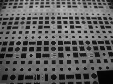
FIGURE 6 Picture of a solar cell wafer with concentrator solar cells of different geometry and grid design.
The potential of grid optimisation on the efficiency of a GaAs single-junction solar cell is visualized in Figure 7 [51]. While the measured solar cell parameters that are linked to the epitaxial layer structure and the antireflective coating were kept constant, the grid design and the solar cell size were optimized for different concentration levels. Efficiency-versus-concentration curves are exemplarily shown for optimized grids for 100, 450, and 1000 suns. The solid line indicates the efficiency that can be reached with the optimal grid and size for each concentration level. Note that a practical minimum size of 1 mm2 is defined here. For comparison, a curve without this size restriction is also shown. The global maximum of 29.09% is reached at 450 suns.
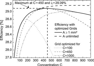
FIGURE 7 Simulated efficiency versus concentration ratio for GaAs solar cells with grid designs optimized for 100, 450, and 1000 suns. In addition, the highest overall efficiency for grid-optimized solar cells with limited (A≥1 mm2) and unlimited cell area is shown. The global efficiency maximum of 29.09% is reached at 450 suns. Note that only the grid structure and the cell size were optimized, whereas the semiconductor layer structure and the antireflection coating of the solar cell were not changed.
(After [51]. Reproduced with permission, © 2010 John Wiley & Sons, Ltd.)
Other challenges for III–V concentrator solar cells include inhomogeneous light profiles caused by the concentrating optics, which can lead to significantly different current densities throughout the solar cell (e.g., [52]). In addition, the tunnel diodes within multijunction solar cells need to be capable of supporting the high current densities (see preceding discussion).
3 III–V Solar Cell Concepts
To further increase the efficiency of III–V multijunction solar cells, various concepts are currently being investigated by research groups around the world. Figure 8 shows the approaches that will be discussed in the following section. Other recent overviews can be found in references [5,53–55]. Note that the schematic drawings are strongly simplified. In reality, each subcell consists of many layers, tunnel junctions are placed between the subcells, metamorphic buffer layers are composed of several layers, and antireflective coatings are placed on top of the device (see Figure 9).

FIGURE 8 Schematic illustration of the III–V solar cell concepts discussed in this chapter. Subcells and metamorphic buffers are indicated. Note that some concepts have also been realized with different materials and band-gap combinations.
The main focus of research nowadays is on III–V multijunction solar cells with three or more junctions, so this chapter emphasizes these concepts. Note, however, that single- and dual-junction solar cells are still also being investigated. What we learn from these simpler devices might help us optimize more complex approaches. For III-V single-junction concentrator solar cells a record efficiency of 29.1% (AM1.5d, 117 suns) was achieved by Fraunhofer ISE with a crystalline GaAs solar cell. With the same material, Alta Devices recently realized a thin-film single-junction solar cell with an efficiency of 28.1% under AM1.5g [2,56]. A record value of 32.6% under 1000 suns (AM1.5d) was achieved by the UPM Madrid with a monolithic Ga0.51In0.49P–GaAs dual-junction solar cell [57]. Note that all recent efficiency records can be found in Green et al. [2]. A historical overview of III–V solar cells can be found in Chapter Id-1 in this book and in references [58,59].
3.1 Lattice-Matched Triple-Junction Solar Cells on Ge
The state-of-the-art III–V solar cell in space and concentrator applications is the lattice-matched Ga0.50In0.50P–Ga0.99In0.01As–Ge triple-junction solar cell, which is shown exemplarily in Figure 9. In this device, all materials have nearly the same lattice constant (see Figure 4), which facilitates achieving good material quality. A champion efficiency of 41.6% (AM1.5d, 364 suns) has already been achieved [60], hence showing the mature status of the lattice-matched approach.
However, the band-gap combination of this device leads to a not optimal split of the solar spectrum, causing a strong excess current in the Ge bottom cell. Therefore, various approaches try to overcome the strong current mismatch by increasing the absorption in the upper two cells (see sections 3.2 and 3.3) or by integrating an additional junction between the GaInAs and the Ge subcell (see section 3.7).
3.2 Quantum Well Solar Cells
The deficiency of high excess current in the bottom cell of the lattice-matched triple-junction solar cell can be partly reduced by implementing quantum wells (QWs) into the middle cell. These can be realized by thin alternating layers of GaAsyP1-y and GaxIn1-xAs (Figure 10(a)) [61]. Quantum wells with a band-gap energy lower than 1.4 eV extend the absorption of the middle cell toward longer wavelengths [62,63]. Thus, the current of the middle cell is increased at the expense of a reduction of the excess current in the Ge bottom cell. The lowest transition energy in the quantum wells and the number of wells determine the current density, which is achievable for the middle cell. However, the open-circuit voltage of QW solar cells is lower than for a cell structure without wells [62]. This drawback can be compensated by the increased current density due to the QWs. Theoretical calculations showed that an overall gain in energy-harvesting efficiency between 3% and 9% relative to the lattice-matched triple-junction solar cell is possible [28]. In addition, QWs are seen as a possibility to tune solar cells for specific spectral conditions [29]. Moreover, it was reported that QW solar cells may lead to higher radiation hardness in space [64].
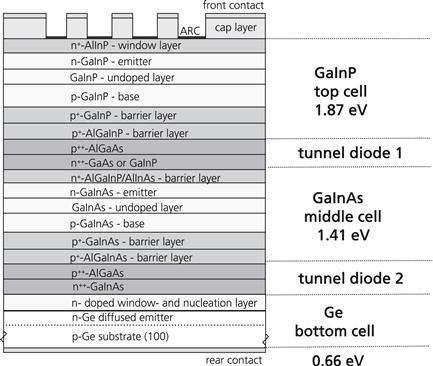
FIGURE 9 Exemplary structure of a monolithic lattice-matched III–V triple-junction solar cell. The band gap of the subcells decreases from top to bottom. The subcells are interconnected in series by tunnel diodes within the device.
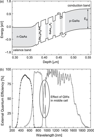
FIGURE 10 (a) Schematic band diagram of four QWs in a GaAs solar cell.
Triple-junction solar cells with quantum wells have already been experimentally realized. Figure 10(b) shows a sample Ga0.50In0.50P–Ga0.99In0.01As–Ge solar cell with 40 QWs in the middle cell [65]. The quantum wells lead to an increase of the EQE of the middle cell linked with a decrease of the bottom cell’s EQE. Therefore, a better current-matching of the subcells can be achieved. For a recent overview about quantum well solar cells, see references [66,67].
3.3 Upright Metamorphic Growth on Ge
As discussed previously, the band-gap combination of the lattice-matched triple-junction is not optimal because it leads to large excess current in the Ge bottom cell. This deficiency originates from the large band-gap difference between the Ga0.99In0.01As middle cell (1.41 eV) and the Ge bottom cell (0.66 eV). Calculations show that lower band gaps for the top and middle cells lead to a higher theoretical efficiency under AM1.5d [69,70] and to higher energy yields [26,27]. As the band gaps of GayIn1-yP and GaxIn1-xAs decrease with increasing In content, these materials can also be used to realize a more optimal band-gap combination. However, an additional technical challenge arises as the lattice constant increases with higher In content (lower band gap, see Figure 4). The monolithic growth of materials with different lattice constants leads to misfit dislocations that deteriorate the material quality. Therefore, lattice-mismatched or metamorphic approaches require adequate strategies to mitigate the effect of dislocations. This is achieved through the implementation of adequate buffer structures between the Ge bottom cell and the GaInAs middle cell [71,72]. These buffer structures increase the lattice constant gradually and hence reduce or confine dislocations as shown in Figure 11(a). A comparison of the external quantum efficiency of a lattice-matched solar cell and a metamorphic triple-junction solar cell is shown in Figure 11(b). The absorption range of the upper two subcells in the metamorphic structure are extended toward longer wavelengths. This leads to higher current generation compared to the lattice-matched structure.
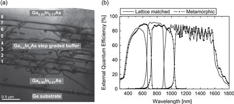
FIGURE 11 (a) Cross-sectional transmission electron micrograph (TEM) of a step-graded Ga1-xInxAs buffer layer grown on Ge. The In content is increased in seven steps from 1% to 17% (1–7) followed by another layer with 20% (8), which helps to fully relax the buffer. (TEM measured at the Christian-Albrechts-University in Kiel, Germany).
Efficiencies above 40% have already been realized with two variants of this approach [70,73], hence proving that the misfit dislocations due to the differences in lattice constant can be handled successfully within the structure. It is also noteworthy that the triple-junction solar cell in reference [70] is well current-matched under AM1.5d. Further improvements can be expected based on the significantly higher theoretical potential of the metamorphic approach in comparison to the lattice-matched approach [26,27].
3.4 Inverted Metamorphic Growth
A challenge of the upright metamorphic concept on Ge is that the lattice mismatch is introduced early in the growth process. Thus, imperfections of the grading buffer can affect the material quality of both upper subcells. To reduce this possible deficiency, research on inverted metamorphic (IMM) growth has been intensified in recent years. In the IMM approach, the growth direction is inverted, hence the top cell is grown first followed by the other subcells (see Figure 12). The substrate is later removed from the top cell using liftoff techniques. This approach allows growing lattice matched on the substrate first, while buffer layers are postponed to later growth phases. Another possible advantage is that the bottom cell is grown epitaxially rather than being created by diffusion into the Ge substrate, hence allowing higher flexibility for the bottom cell band gap. Geisz et al. [75] presented an IMM structure with an efficiency of 40.8% (AM1.5d, 326 suns). The Ga0.51In0.49P top cell (1.83 eV) was grown lattice matched on a GaAs substrate. A buffer is then used to increase the lattice constant by 0.3% for the Ga0.96In0.04As middle cell (1.34 eV) followed by another buffer for the Ga0.63In0.37As bottom cell (0.89 eV, 2.6% misfit). Several other IMM designs are also investigated, e.g., in [76–79]. With subcells of GaInP (1.9 eV), GaAs (1.4 eV) and GaInAs (1.0 eV) Cornfeld et al. [76] reached an efficiency of 32% under AM0 (1367 W/m2), while Takamoto et al. [79] achieved an efficiency of 35.8% under AM1.5 g (1000 W/m2).

FIGURE 12 Scheme of the production process of IMM solar cells. The epitaxial structure is grown inverted to the conventional growth direction. The first two subcells can hence be grown lattice matched to the GaAs or Ge substrate. A metamorphic buffer gradually increases the lattice constant for the subcell that is grown last. The substrate is then removed using liftoff techniques. Finally, the epitaxial structure is processed to solar cells.
(Illustration inspired by [79].)
A possible drawback for the IMM approach compared to Ge-based structures is the higher complexity of cell processing connected with substrate removal, which may lead to higher production costs and low yield. Yet these disadvantages might be counterbalanced by lower material costs if the substrate can be reused. Another benefit of the IMM structure in particular for space application is their possible lower weight and the chance to realize flexible devices.
3.5 Bifacial Growth
Another approach that deviates from the conventional growth direction is bifacial growth [80], which recently led to an efficiency of 42.3% (AM1.5d, 406 suns) [81]. The specific feature is that subcells are grown on both sides of a GaAs substrate. First, a graded buffer is grown on the backside of a GaAs wafer followed by a GaInAs bottom cell (0.95 eV). The wafer is then flipped within the MOVPE reactor, and a tunnel junction, a GaAs middle cell (1.42 eV), another tunnel junction, and a GaInP top cell (1.89 eV) are grown. The advantage of this approach is that the two upper cells can be grown lattice matched to the GaAs substrate. In addition, the thick substrate protects the upper two cells from dislocations originating from the lattice-mismatched GaInAs bottom cell. The complexity of cell processing is similar to upright metamorphic approaches.
3.6 III–V on Si
Since the early 90s research efforts have been ongoing to grow III–V solar cells on silicon substrates (1.1 eV), e.g., [82–84]. The interest in this field has increased in recent years in order to replace the expensive Ge substrate of today’s lattice-matched triple-junction solar cells with lower-cost Si. Moreover, the higher band gap of Si compared with Ge leads to an increase of the theoretical energy-harvesting efficiency by 3% [28].
The main challenges here are to overcome the 4.1% difference in lattice constant between Si and GaAs and to handle the difference in thermal expansion coefficient. In general, two different approaches need to be distinguished: direct growth on the Si substrate and wafer bonding. The first approach requires strategies to ensure sufficient material quality in the III–V subcells. As it is extremely challenging to achieve good material quality for direct GaAs growth on Si (e.g., [83,85]) different buffer layers are investigated to increase the lattice constant gently. Several of the investigated strategies are shown in Figure 13. GaAs or GaInP solar cells on Si substrates have already been demonstrated (e.g., [86–89]). Research efforts are continuing to realize III–V triple-junction solar cells on Si with efficiencies close to the potential of this approach.
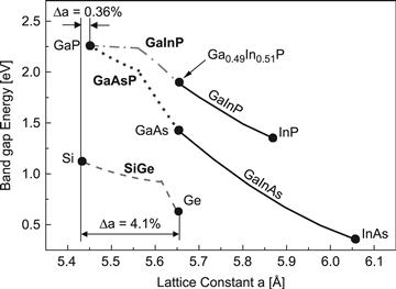
FIGURE 13 Different strategies to overcome the 4.1% difference in lattice constant between GaAs and Si. One option is to first create a Ge layer either directly or through the use of SiGe compounds to transfer from Si to Ge (e.g., [87,90,91]). Other options are to use Ga1-xInxP or GaAsxP1-x buffers on a GaP nucleation (e.g., [92–95]).
(Graphic from [94]. Reproduced with permission.)
The necessity of a suitable buffer can be avoided by using dilute nitrides (GaIn)(NAsP). This material system offers a wide band-gap range from 1 eV to 2 eV and allows choosing materials that are lattice matched to Si. Yet this promising approach has been limited so far by the short minority-carrier diffusion length of the dilute nitrides (e.g., [96–98]).
The use of wafer-bonding [53,99,100] relaxes the challenge of realizing a transition buffer as the silicon bottom cell and the upper subcells (e.g., a GaInP–GaAs dual-junction solar cell) are grown independently and then combined through wafer bonding. After the bonding process, the substrate of the upper two solar cells is removed by using liftoff techniques such as ion implantation [101] and laser [102], stress-induced [103], or wet chemical liftoff [104]. Both the liftoff process and the bonding lead to technological challenges. However, promising result have already been achieved (e.g., [105–107]). Recently, a GaInP–GaAs–Si triple-junction solar cell with an efficiency of 23.3% under AM1.5d (24 suns) has been demonstrated at Fraunhofer ISE [108]. It was realized through wafer bonding of a GaInP–GaAs dual-junction and a silicon solar cell.
3.7 More Than Three Junctions
As shown in Figure 3, the theoretical efficiency limit of a multijunction solar cell under reference conditions increases with the number of junctions. For applications with rather stable spectral conditions such as satellites in Earth orbit, this trend directly translates into higher efficiencies. Yet under real operating conditions on Earth or other planets like Mars [34], spectral changes throughout the day and year need to be taken into account. To evaluate the effect of an additional junction on the energy yield, the energy-harvesting efficiency can be studied, for example, using a model as presented in reference [26]. Figure 14 shows the energy-harvesting efficiency and the optimal band-gaps for multijunction solar cells with up to six p–n junctions for the varying spectral conditions at three exemplary locations [28]. For all three locations, the energy-harvesting efficiency increases steadily from three to six junctions. Thus, even under varying spectral conditions, a higher power output for solar cells with increasing number of subcells can be expected. However, the benefits of adding more junctions become smaller: adding a fourth junction leads to 5% higher efficiencies on average, whereas a fifth junction only adds another 3% to the energy-harvesting efficiency. It needs to be taken into account that the model assumes ideal solar cells. Therefore, it is an open question if the small theoretically expected gain in energy yield for solar cells with more than four junctions can be achieved in reality. Another important point to note is that the ideal band-gap energies at the three locations only vary by 10–20 meV. This indicates that it is not necessary to develop a different solar cell for each operating site.
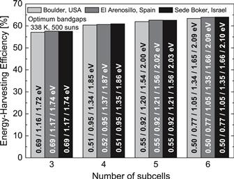
FIGURE 14 Calculated energy-harvesting efficiency of ideal multijunction solar cells with three to six junctions for three different locations on Earth. Calculations are performed for a concentration factor of 500 suns and a cell temperature of 338 K. Spectral influences of the concentrator optics are not taken into account. The optimum combination of band-gap energies is given for each number of junctions.
(After [28]. Reproduced with permission, © 2010 IEEE.)
One straightforward approach for III–V multijunction solar cells with more than three junctions is to grow lattice matched on Ge substrates. Starting from the standard lattice-matched Ga0.50In0.50P–Ga0.99In0.01As–Ge solar cell, theoretical calculations show that a 1-eV fourth junction placed above the Ge bottom cell could boost the efficiency significantly. Research efforts are ongoing to realize such a junction with the quaternary alloy GaInNAs [60,96,109–111]. Yet up to now, the subcell suffers from a low minority-carrier diffusion length, leading to current limitation in a four-junction solar cell. One way to work around this deficiency is to use a five- or six-junction configuration with a smaller current of each subcell. Such a device can be realized by adding subcells of AlGaInP and AlGaInAs. Figure 15(a) shows the internal quantum efficiency of such a six-junction solar cell, which was recently realized at Fraunhofer ISE [111]. Note that the complex device is composed of more than 40 semiconductor layers, leaving large room for ongoing optimisation. The IV characteristic of the six-junction solar cell under AM0 is compared with those of triple- and four-junction solar cells in Figure 15(b). The voltage increases with the number of junctions, while the current decreases. The IV characterisation of the four- and six-junction solar cells was performed under a novel flash simulator with six independently variable light channels, which allows the spectrum to be adjusted for each junction.
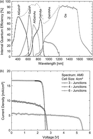
FIGURE 15 (a) Measured internal quantum efficiency of an AlGaInP–GaInP–AlGaInAs– GaInAs–GaInNAs–Ge six-junction solar cell. (b) Comparison of measured IV characteristic under AM0 of the six-junction solar cell with a GaInP–GaAs–Ge triple-junction and an AlGaInP–GaInAs–GaInNAs–Ge four-junction solar cell.
(Both graphs after [111]. Reproduced with permission.)
An option for a lattice-matched five-junction solar cell is to include junctions of AlGaInP and AlGaInAs into a lattice-matched triple-junction solar cell [112,113]. The main benefit of this structure is that the thickness of the subcells is significantly reduced. Thus, a low minority-carrier lifetime has a comparably smaller impact, which improves the radiation hardness of the device. In addition, only well-known materials are used in this structure. Another approach, which is lattice matched to Ge, is the AlGaInP–AlGaInAs–GaInAs–Ge (1.95 eV, 1.66 eV, 1.39 eV, and 0.72 eV, respectively) four-junction solar cell realized by King et al. [60]. A prototype device already achieved an efficiency of about 37% (AM1.5d, 500 suns) in preliminary measurements.
A different route to realizing III–V solar cells with more than three junctions is to use inverted metamorphic [77,114] or semiconductor-bonding techniques [115]. Cornfeld et al. [116] presented an inverted metamorphic four-junction solar cell that recently reached an in-house measured efficiency above 34% under AM0 [3]. A bottom cell of GaInAs (0.7 eV) was added to a formerly developed inverted metamorphic triple-junction solar cell [76]. Another metamorphic buffer was implemented to accommodate the additional 2% lattice mismatch. Moreover, designs for inverted metamorphic solar cells with five and six junctions have also been proposed [3,60].
Law et al. [115] realized a 31.7% (AM0) five-junction solar cell using a direct semiconductor-bonding technique. The three upper subcells—AlGaInP (2.0 eV), AlGa(In)As (1.7 eV), and Ga(In)As (1.4 eV)—were grown inverted on GaAs or Ge substrates, while a InP substrate was used for the upright growth of the two lower subcells consisting of GaInPAs (1.1 eV) and GaIn(P)As (0.8 eV). The epitaxial wafers are then bonded together using semiconductor-bonding techniques. An advantage of this approach is that all subcells are grown lattice matched to the corresponding substrate. Recently, an AM0 efficiency of around 31% was presented for a semiconductor-bonded four-junction solar cell with a band-gap combination of 1.9–1.4–1.0–0.73 eV [78].
3.8 Other Approaches
The challenge of current matching in monolithic multijunction solar cells can be circumvented by using optical beam splitting (for a detailed review, see Imnes et al. [117]). In a spectrum-splitting architecture, spectrally selective filters are used to split the incident solar radiation and to direct the light toward different single- or dual-junction solar cells, which are individually designed for the corresponding wavelength range. This allows realizing optimal band-gap combinations without the usual constraints of lattice or current matching. A light-splitting approach was already experimentally realized in 1978 by Moon et al. [118] and has found increasing interest again in recent years due to progress in dichroic filter technology [119–122]. Theoretical calculations of the energy-harvesting efficiency showed that an optical beam splitting approach with a GaInP–GaAs (1.87–1.41 eV), a Si (1.10 eV), and a GaSb (0.7 eV) solar cell has a theoretical potential that is 18% higher than theoretical values for a lattice-matched GaInP–GaInAs–Ge solar cell [28]. Another recent theoretical study also presented the result that operating efficiencies of solar cell arrays with two to four cells are expected to be higher in a spectral-splitting approach than for series interconnection [123]. Several spectral-beam splitting receivers have recently been realized showing promising efficiencies [120–122,124,125]. The devices are still in a prototype stage. Further optimisation of these rather complex structures as well as steps toward mass production must be undertaken.
Another approach for optimal band-gap combinations are nanowire solar cells in which materials with different lattice constants can be combined in high material quality. The small diameter of the wires allows the strain from the lattice mismatch to relax by an expansion or contraction of the nanowires to the side [126]. Another advantage of this approach is that expensive III–V substrate material can be saved by growing the III–V nanowires on Si substrates or solar cells [127,128]. Nanowire solar cells are still in the development phase. However, theoretical [126,129] and experimental [130,131] investigations of different solar cell designs show promising results.
Several other approaches use nanostructures for photovoltaics. Some of these could also be used for III–V solar cells. An overview can be found in reference [132].
4 Conclusions
III–V multijunction solar cells have already reached efficiencies above 40% and a further increase toward 50% can be expected. These devices are widely used in space applications and terrestrial concentrators as well as in several niche applications. The great choice of III–V semiconductor materials allows various design options, several of which are currently being investigated, while others remain to be explored in the future. Material availability, quality, and manufacturing complexity will finally determine the most successful approaches for achieving optimum performance.
Acknowledgements
The authors thank all members of the department III–V—Epitaxy and Solar Cells at Fraunhofer ISE for their contributions to the work presented here. The authors especially appreciate the very helpful contributions of Stephanie Essig, Peter Kailuweit, René Kellenbenz, Vera Klinger, Tobias Roesener, Marc Steiner, and Wolfram Wettling.
References
1. Green MA, Emery K, King DL, Igari S, Warta W. Solar cell efficiency tables (Version 01). Prog Photovolt: Res Appl. 1993;12:55–62.
2. Green MA, Emery K, Hishikawa Y, Warta W, Dunlop ED. Solar cell efficiency tables (Version 38). Prog Photovolt: Res Appl. 2011;19:565–572.
3. Patel P, Aiken D, Boca A, et al. Experimental results from performance improvement and radiation hardening of inverted metamorphic multi-junction solar cells. Seattle, Washington: Proceedings of the 37th IEEE Photovoltaics Specialists Conference; 2011; in press.
4. Bailey S, Raffaelle R. Space solar cells and arrays. In: Luque A, Hegedus S, eds. Handbook of Photovoltaic Science and Engineering. Chichester, West Sussex, UK: John Wiley & Sons, Ltd.; 2011;:365–401. .
5. Friedman DJ, Olson JM, Kurtz S. High-efficiency III–V multijunction solar cells. In: Luque A, Hegedus S, eds. Handbook of Photovoltaic Science and Engineering. Chichester, West Sussex, UK: John Wiley & Sons, Ltd.; 2011;:314–364. .
6. Bailey SG, Raffaelle R, Emery K. Space and terrestrial photovoltaics: synergy and diversity. Prog Photovolt: Res Appl. 2002;10 399–306.
7. Luque A, Andreev VM. Concentrator Photovoltaics. Heidelberg, Germany: Springer Verlag; 2007; 345.
8. Pérez-Higuerasa P, Muñoz E, Almonacida G, Vidala PG. High Concentrator PhotoVoltaics efficiencies: present status and forecast. Renew Sustain Energy Rev. 2011;15.
9. Andreev VM. Solar cells for TPV converters. In: Next Generation Photovoltaics: High Efficiency Through Full Spectrum Utilization. St. Petersburg, Russia: Institute of Physics Publishing; 2004;:246–273. .
10. Coutts TJ. A review of progress in thermophotovoltaic generation of electricity. Renew Sustain Energy Rev. 1999;77–184.
11. Andreev V, Khvostikov V, Vlasov A. Solar thermophotovoltaics. In: Luque A, Andreev V, eds. Concentrator Photovoltaics. Heidelberg, Germany: Springer Verlag; 2007;175–198.
12. Bauer T. Thermophotovoltaics: Basic Principles and Critical Aspects of System Design. Berlin, Germany: Springer; 2011; p. 222.
13. Wojtczuk SJ. Long-wavelength laser power converters for optical fibers. Anaheim, CA: Proceedings of the 26th IEEE Photovoltaic Specialists Conference; 1997; pp. 971–974.
14. Krut D, Sudharsanan R, Nishikawa W, Issiki T, Ermer J, Karam NH. Monolithic multi-cell GaAs laser power converter with very high current density. New Orleans: Proceedings of the 29th IEEE Photovoltaics Specialists Conference; 2002; pp. 908–911.
15. Andreev V, Khvostikov V, Kalinovsky V, et al. High current density GaAs and GaSb photovoltaic cells for laser power beaming. Osaka, Japan: Proceedings of the 3rd World Conference on Photovoltaic Energy Conversion; 2003; pp. 761–764.
16. Werthen JG. Powering next generation networks by laser light over fiber. San Diego, CA: Proceedings of the conference on optical fiber communication; 2008; pp. 2881–2883.
17. Oliva E, Dimroth F, Bett AW. GaAs converters for high power densities of laser illumination. Prog Photovolt: Res Appl. 2008;4:289–295.
18. Schubert J, Oliva E, Dimroth F, Guter W, Loeckenhoff R, Bett AW. High- voltage GaAs photovoltaic laser power converters. IEEE Trans Electron Dev. 2009;56:170–175.
19. Böbner G, Dreschmann M, Klamouris C, et al. An optically powered video camera link, IEEE Photon. Tech Lett. 2008;20:39–41.
20. ASTM E490–00a Standard Solar Constant and Zero Air Mass Solar Spectral Irradiance Tables. American Society for Testing and Materials 2000.
21. ASTM-G173 Standard Tables for Reference Solar Spectral Irradiances: Direct Normal and Hemispherical on 37 Tilted Surface. ASTM 2008.
22. Kurtz SR, Myers D, McMahon WE, Geisz J, Steiner M. A comparison of theoretical efficiencies of multi-junction concentrator solar cells. Prog Photovolt: Res Appl. 2008;16:537–546.
23. Shockley W, Queisser HJ. Detailed balance limit of efficiency of p–n junction solar cells. J Appl Phys. 1961;vol. 32:510–519.
24. Létay G, Bett AW. EtaOpt—a program for calculating limiting efficiency and optimum bandgap structure for multi-bandgap solar cells and TPV cells. Munich, Germany: Proceedings of the 17th European Photovoltaic Solar Energy Conference; 2001; pp. 178–181.
25. Kinsey GS, Edmondson KM. Spectral response and energy output of concentrator multijunction solar cells. Prog Photovolt: Res Appl. 2009;17:279–288.
26. Philipps SP, Peharz G, Hoheisel R, et al. Energy harvesting efficiency of III–V triple-junction concentrator solar cells under realistic spectral conditions. Sol Energy Mater Sol Cells. 2010;94:869–877.
27. Philipps SP, Peharz G, Hoheisel R, et al. Energy harvesting efficiency of lll–V multi-junction concentrator solar cells under realistic spectral conditions. Freiburg, Germany: Proceedings of the 6th International Conference on Concentrating Photovoltaic Systems; 2010; pp. 294–298.
28. Dimroth F, Philipps SP, Welser E, et al. Promises of advanced multi-junction solar cells for the use in CPV systems. Honolulu, Hawai: Proceedings of the 35th IEEE Photovoltaics Specialists Conference; 2010; pp. 1231–1236.
29. Norton M, Dobbin A, Phinikarides A, Tibbits T, Georghiou GE, Chonavel S. Field performance evaluation and modelling of spectrally tuned quantum-well solar cells. Seattle, Washington: Proceedings of the 37th IEEE Photovoltaics Specialists Conference; 2011; in press.
30. Kurtz SR, Olson JM, Faine P. The difference between standard and average efficiencies of multijunction compared with single-junction concentrator cells. Sol Energy Mater Sol Cells. 1991;30:501–513.
31. Faine P, Kurtz SR, Riordan C, Olson JM. The influence of spectral solar irradiance variations on the performance of selected single-junction and multijunction solar cells. Sol Cells. 1991;31:259–278.
32. Araki K, Yamaguchi M. Influences of spectrum change to 3-junction concentrator cells. Sol Energy Mater Sol Cells. 2003;75:707–714.
33. Peharz G, Siefer G, Bett AW. A simple method for quantifying spectral impacts on multi-junction solar cells. Sol Energy. 2009;83:1588–1598.
34. Hoheisel R, Philipps SP, Bett AW. Long-term energy production of III–V triple- junction solar cells on the Martian surface. Prog Photovolt: Res Appl. 2010;18:90–99.
35. Bett AW, Dimroth F, Stollwerck G, Sulima OV. III–V compounds for solar cell applications. Appl Phys. 1999;69:119–129.
36. Fraas LM, Avery JE, Martin J, et al. Over 35-percent efficient GaAs/GaSb tandem solar cells. IEEE Trans Electron Dev. 1990;37:443–449.
37. Andreev VM, Karlina LB, Kazantsev AB, et al. Concentrator tandem solar cells based on AlGaAs/GaAs-InP/ InGaAs(or GaSb) structures. Hawaii, USA: Proceedings of the 1st World Conference on Photovoltaic Energy Conversion; 1994; pp. 1721–1724.
38. Takamoto T, Ikeda E, Agui T, et al. InGaP/ GaAs and InGaAs mechanically stacked triple junction solar cells. Anaheim, California, USA: Proceedings of the 26th IEEE Photovoltaic Specialists Conference; 1997; pp. 1031–1034.
39. Bett AW, Baur C, Beckert R, et al. Development of high-efficiency mechanically stacked GaInP/GaInAs-GaSb triple-junction concentrator solar cells. Munich, Germany: Proceedings of the 17th European Photovoltaic Solar Energy Conference; 2001; pp. 84–87.
40. Esaki L. New phenomenon in narrow Germanium p-n junction. Phys Rev. 1958;109:603–604.
41. Hermle M, Létay G, Philipps SP, Bett AW. Numerical simulation of tunnel diodes for multi-junction solar cells. Prog Photovolt: Res Appl. 2008;16:409–418.
42. Meusel M, Baur C, Létay G, Bett AW, Warta W, Fernandez E. Spectral response measurements of monolithic GaInP/Ga(In)As/Ge triple-junction solar cells: measurement artifacts and their explanation. Prog Photovolt: Res Appl. 2003;11:499–514.
43. Baur C, Hermle M, Dimroth F, Bett AW. Effects of optical coupling in III–V multilayer systems. Appl Phys Lett. 2007;90 192109/1–192109/3.
44. Siefer G, Baur C, Bett AW. External quantum efficiency measurements of germanium bottom subcells: measurement artifacts and correction procedures. HI: Proceedings of the 35th IEEE Photovoltaic Specialists Conference Honolulu; 2010; pp. 704– 707.
45. Li J-J, Lim SH, Allen CR, Ding D, Zhang Y-H. Combined effects of shunt and luminescence coupling on external quantum efficiency measurements of multi- junction solar cells. Seattle, Washington: Proceedings of the 37th IEEE Photovoltaics Specialists Conference; 2011; in press.
46. Bett AW, Dimroth F, Siefer G. Multijunction concentrator solar cells. In: Luque A, Andreev V, eds. Concentrator Photovoltaics. Heidelberg, Germany: Springer Verlag; 2007;67–87.
47. Moore AR. An optimized grid design for a sun-concentrator solar cell. RCA Review. 1979;40:140–151.
48. Nubile P, Veissid N. A contribution to the optimization of front-contact grid patterns for solar cells. Solid-State Electron. 1994;37:220–222.
49. Rey-Stolle I, Algora C. Modeling of the resistive losses due to the bus-bar and external connections in III–V high-concentrator solar cells. IEEE Trans Electron Dev. 2002;49:1709–1714.
50. Galiana B, Algora C, Rey-Stolle I, Vara IG. A 3-D model for concentrator solar cells based on distributed circuit units. IEEE Trans Electron Dev. 2005;52:2552–2558.
51. Steiner M, Philipps SP, Hermle M, Bett AW, Dimroth F. Validated front contact grid simulation for GaAs solar cells under concentrated sunlight. Prog Photovolt: Res Appl. 2010;19:73–83.
52. Algora C. Very-high-concentration challenges of III–V multijunction solar cells. In: Luque A, Andreev V, eds. Concentrator Photovoltaics. Heidelberg, Germany: Springer Verlag; 2007;89–111.
53. Law DC, King RR, Yoon H, et al. Future technology pathways of terrestrial III–V multijunction solar cells for concentrator photovoltaic systems. Sol Energy Mater Sol Cells. 2008;94:1314–1318.
54. Friedman DJ. Progress and challenges for next-generation high-efficiency multijunction solar cells. Curr Opin Solid State Mater Sci. 2010;14:131–138.
55. Philipps SP, Guter W, Welser E, et al. Present status in the development of III–V multi-junction solar cells. In: Luque L, Martí A, Cristóbal AB, eds. New Concepts for a Next Generation of Photovoltaics. Berlin, Germany: Springer, to be published; 2011.
56. Kayes BM, Nie H, Twist R, Spruytte SG. 27.6% conversion efficiency, a new record for single-junction solar cells under 1 sun illumination. Seattle, Washington: Proceedings of the 37th IEEE Photovoltaics Specialists Conference; 2011; in press.
57. Garcia I, Rey-Stolle I, Galiana B, Algora C. A 32.6 percent efficient lattice- matched dual-junction solar cell working at 1000 suns. Appl Phys Lett. 2009;94:053509.
58. Sharps PR, Stan MA, Aiken DJ, Newman FD, Hills JS, Fatemi NS. High efficiency multi-junction solar cells – past, present, and future. Paris, France: Proceedings of the 19th European Photovoltaic Solar Energy Conference; 2004; pp. 3569–3574.
59. Alferov ZI, Andreev VM, Rumyantsev VD. III–V heterostructures in photovoltaics. In: Luque A, Andreev V, eds. Concentrator Photovoltaics. Heidelberg, Germany: Springer Verlag; 2007;25–50.
60. King R, Boca A, Hong W, et al. Band-gap-engineered architectures for high-efficiency multijunction concentrator solar cells. Hamburg, Germany: Proceedings of the 24th European Photovoltaic Solar Energy Conference and Exibition; 2009; pp. 55–61.
61. Barnham KWJ, Ballard I, Connolly JP, et al. Quantum well solar cells. Physica. 2002;14:27–36.
62. Barnham K, Ballard I, Barnes J, et al. Quantum well solar cells. Appl Surf Sci 113–114 1997;722–733.
63. Ekins-Daukes NJ, Barnham KWJ, Connolly JP, et al. Strain-balanced GaAsP/InGaAs quantum well solar cells. Appl Phys Lett. 1999;75:4195–4197.
64. Walters RJ, Summers GP, Messenger SR, Freundlich A, Monier C, Newman F. Radiation hard multi-quantum well InP/InAsP solar cells for space applications. Prog Photovolt: Res Appl. 2000;8:349–354.
65. Kellenbenz R, Hoheisel R, Kailuweit P, Guter W, Dimroth F, Bett AW. Development of radiation hard Ga0.50In0.50P/Ga0.99In0.01As/Ge spase solar cells with multi quantum wells. Honolulu, Hawai: Proceedings of the 35th IEEE Photovoltaic Specialists Conference; 2010; pp. 117–122.
66. Barnham KWJ, Ballard IM, Browne BC, et al. Recent progress in quantum well solar cells. In: Tsakalakos L, ed. Nanotechnology for Photovoltaics. Boca Raton, Florida, USA: CRC Press; 2010;187–210.
67. Adams JGJ, Browne BC, Ballard IM, et al. Recent results for single-junction and tandem quantum well solar cells. Prog Photovolt: Res Appl. 2011; in press.
68. Kailuweit P, Kellenbenz R, Philipps SP, Guter W, Bett AW, Dimroth F. Numerical simulation and modeling of GaAs quantum-well solar cells. J Appl Phys. 2010;107 064317-1–064317–6.
69. Dimroth F, Beckert R, Meusel M, Schubert U, Bett AW. Metamorphic GayIn1- yP/Ga1-xInxAs tandem solar cells for space and for terrestrial concentrator applications at C.1000 suns. Prog Photovolt: Res Appl. 2001;9:165–178.
70. Guter W, Schöne J, Philipps SP, et al. Current- matched triple-junction solar cell reaching 41.1% conversion efficiency under concentrated sunlight. Appl Phys Lett. 2009;94 223504-1–223504–3.
71. Bett AW, Baur C, Dimroth F, Schöne J. Metamorphic GaInP-GaInAs layers for photovoltaic applications. Mater Res Soc Symp Proc. 2005;836:223–234.
72. Schöne J, Spiecker E, Dimroth F, Bett AW, Jäger W. Misfit dislocation blocking by Dilute Nitride intermediate layers. Appl Phys Lett. 2008;92:081905.
73. King RR, Law DC, Edmondson KM, et al. 40% efficient metamorphic GaInP/GaInAs/Ge multijunction solar cells. Appl Phys Lett. 2007;90 183516-1–183516–3.
74. Dimroth F, Kurtz S. High-efficiency multijunction solar cells. MRS Bull. 2007;32:230–234.
75. Geisz JF, Friedman DJ, Ward JS, et al. 40.8% efficient inverted triple-junction solar cell with two independently metamorphic junctions. Appl Phys Lett. 2008;93 123505-1–123505–3.
76. Cornfeld AB, Stan M, Varghese T, et al. Development of a large area inverted metamorphic multi-junction (IMM) highly efficient AM0 solar cell. San Diego: Proceedings of the 33rd IEEE Photovoltaic Specialists Conference; 2008; pp. 26/1–5.
77. Yoon H, Haddad M, Mesropian S, et al. Progress of inverted metamorphic III–V solar cell development at Spectrolab. San Diego, USA: Proceedings of the 33rd IEEE Photovoltaic Specialists Conference; 2008; pp. 25/1–6.
78. Boisvert J, Law D, King R, et al. Development of advanced space solar cells at Spectrolab. Honolulu, Hawaii, USA: Proceedings of the 35th IEEE Photovoltaic Specialists Conference; 2010; pp. 123–127.
79. Takamoto T, Agui T, Yoshida A, et al. World’s highest efficiency triple-junction solar cells fabricated by inverted layers transfer process. Honolulu, Hawai: Proceedings of the 35th IEEE Photovoltaics Specialists Conference; 2010; pp. 412–417.
80. Wojtczuk S, Chiu P, Zhang X, et al. InGaP/ GaAs/InGaAs 41% concentrator cells using bi-facial epigrowth. Honolulu, Hawai: Proceedings of the 35th IEEE Photovoltaics Specialists Conference; 2010; pp. 1259–1264.
81. Chiu P, Wojtczuk S, Harris C, Pulver D, Timmons M. 42.3% efficient InGaP/ GaAs/InGaAs concentrators using bifacial epigrowth. Seattle, Washington: Proceedings of the 37th IEEE Photovoltaics Specialists Conference; 2011; in press.
82. Yamaguchi M, Amano C. Efficiency calculations of thin-film GaAs solar cells on Si substrates. J Appl Phys. 1985;58:3601–3606.
83. Fang SF, Adomi K, Iyer S, et al. Gallium arsenide and other compound semiconductors on Silicon. J Appl Phys. 1990;68:R31–58.
84. Bett AW, Borgwarth K, Schetter C, Sulima OV, Wettling W. GaAs-on-Si solar cell structures grown by MBE and LPE. New Delhi, India: Proceedings of the 6th International Photovoltaic Scinece and Engineering Concerence; 1992; pp. 843–847.
85. Ahrenkiel RK, Al Jassim MM, Keyes B, et al. Minority carrier lifetime of GaAs on silicon. J Electrochem Soc. 1990;137:996–1000.
86. Hayashi K, Soga T, Nishikawa H, Jimbo T, Umeno M. MOCVD growth of GaAsP on Si for tandem solar cell application. Waikoloa, Hawai: Proceedings of the 35th IEEE Photovoltaics Specialists Conference; 1994.
87. Ringel SA, Carlin JA, Andre CL, et al. Single-junction InGaP/GaAs solar cells grown on Si substrates with SiGe buffer layers. Prog Photovolt: Res Appl. 2002;10:417–426.
88. Lueck MR, Andre CL, Pitera AJ, Lee ML, Fitzgerald EA, Ringel SA. Dual junction GaInP/GaAs solar cells grown on metamorphic SiGe/Si substrates with high open circuit voltage. IEEE Electron Dev Lett. 2006;27:142–144.
89. Geisz JF, Olson JM, Romero MJ, Jiang CS, Norman AG. Lattice-mismatched GaAsP solar cells grown on Silicon by OMVPE. Waikoloa, Hawaii, USA: Proceedings of the 4th World Conference on Photovoltaic Energy Conversion; 2006; pp. 772–775.
90. Colace L, Masini G, Galluzzi F, et al. Metal–semiconductor–metal near-infrared light detector based on epitaxial Ge/Si. Appl Phys Lett. 1998;72:3175–3177.
91. Park J-S, Curtin M, Bai J, Carrol M, Lochtefeld A. Growth of Ge thick layers on Si(001) substrates using reduced pressure chemcial vapor deposition. Jpn J Appl Phys. 2006;45:8581–8585.
92. Grassman TJ, Brenner MR, Gonzalez M, et al. Characterization of metamorphic GaAsP/Si materials and devices for photovoltaic applications. IEEE Trans Electron Dev. 2010;57:3361–3369.
93. Döscher H, Hannappel T. In situ reflection anisotropy spectroscopy analysis of heteroepitaxial GaP films grown on Si(100). J Appl Phys. 2010;107:123523.
94. Roesener T, Döscher H, Beyer A, et al. MOVPE growth of III-V solar cells on Silicon in 300mm closed coupled showerhead reactor. Valencia, Spain: Proceedings of the 25th European Photovoltaic Solar Energy Conference and Exhibition; 2010; pp. 964–968.
95. Volz K, Beyer A, Witte W, et al. GaP- nucleation on exact Si (001) substrates for III/V device integration. J Cryst Growth. 2011;315:37–47.
96. Kondow M, Uomi K, Niwa A, Kitatani T, Watahiki S, Yazawa Y. GaInNAs: a novel material for long-wavelength-range laser diodes with excellent high-temperature performance. Jpn J Appl Phys. 1996;35:1273–1275.
97. Geisz JF, Friedman DJ. III-N-V semiconductors for solar photovoltaic applications. Semicond Sci Technol. 2002;17:769–777.
98. Volz K, Stolz W, Teubert J, et al. Doping, electrical properties and solar cell application of GaInNAs. In: Ayse E, ed. Dilute III–V Nitride Semiconductors and Material Systems. Heidelberg: Springer Berlin Heidelberg; 2008;369–404.
99. Tong Q-Y, Gösele U. Semiconductor Wafer Bonding: Science and Technology. New York, New York, USA: John Wiley & Sons, Inc.; 1999; p. 297.
100. Reiche M. Semiconductor wafer bonding. Phys Status Solidi. 2006;203:747–759.
101. Mayer JW. Ion implantation in semiconductors. International Electron Devices Meeting 1973; pp. 3–5.
102. Kelly MK, Ambacher O, Dimitrov R, Handschuh R. Stutzmann, Optical process for liftoff of group III-nitride films. Phys Status Solidi (a). 1997;159:R3–R4.
103. Dross F, Robbelein J, Vandevelde B, et al. Stress-induced large-area lift-off of crystalline Si films. Appl Phys A: Mater Sci Process. 2007;89:149–152.
104. Demeester P, Pollentier I, De Dobbelaere P, Brys C, Van Daele P. Epitaxial lift-off and its applications. Semicond Sci Technol. 1993;8:1124–1135.
105. Fontcuberta i Morral A, Zahler JM, Atwater HA, Ahrenkiel SP, Wanlass MW. InGaAs/InP double heterostructures on InP/Si templates fabricated by wafer bonding and hydrogen-induced exfoliation. Appl Phys Lett. 2003;83:5413.
106. Zahler JM, Tanabe K, Ladous C, Pinnington T, Newman FD, Atwater HA. High efficiency InGaAs solar cells on Si by InP layer transfer. Appl Phys Lett. 2007;91:012108.
107. Archer MJ, Law DC, Mesropian S, et al. GaInP/GaAs dual junction solar cells on Ge/Si epitaxial templates. Appl Phys Lett. 2008;92:103503.
108. Dreyer K, Fehrenbacher E, Oliva E, et al. GaInP/GaAs/Si triple-junction solar cell formed by wafer bonding. DPG Spring Meeting, Dresden, Germany 2011.
109. Volz K, Lackner D, Nemeth I, et al. Optimization of annealing conditions of (GaIn)(NAs) for solar cell applications. J Cryst Growth. 2008;310:2222–2228.
110. Kurtz S, Johnston SW, Geisz JF, Friedman DJ, Ptak AJ. Effect of nitrogen concentration on the performance of Ga1-xInxNyAs1-y solar cells. Orlando, Florida, USA: Proceedings of the 31st IEEE Photovoltaic Specialists Conference; 2005; pp. 595–598.
111. Essig S, Stämmler E, Rönsch S, et al. Dilute nitrides for 4- and 6-junction space solar cells. Saint Raphaël, France: Proceedings of the 9th European Space Power Conference; 2011; in press.
112. Dimroth F, Schubert U, Bett AW, et al. Next generation GaInP/GaInAs/Ge multi-junction space solar cells. Munich, Germany: Proceedings of the 17th European Photovoltaic Solar Energy Conference; 2001; pp. 2150–2154.
113. Dimroth F, Meusel M, Baur C, Bett AW, Strobl G. 3–6 junction photovoltaic cells for space and terrestrial concentrator applications. Orlando, Florida, USA: Proceedings of the 31st IEEE Photovoltaic Specialists Conference; 2005; pp. 525–529.
114. Friedman DJ, Geisz JF, Norman AG, Wanlass MW, Kurtz SR. 0.7-eV GaInAs junction for a GaInP/GaAs/GaInAs(1eV)/GaInAs(0.7eV) four-junction solar cell. Waikoloa, Hawaii, USA: Proceedings of the 4th World Conference on Photovoltaic Energy Conversion; 2006; pp. 598–602.
115. Law DC, Bhusari DM, Mesropian S, et al. Semiconductor-bonded III–V multi-junction space solar cells. Philadelphia, USA: Proceedings of the 34th IEEE Photovoltaic Solar Energy Conference; 2009; pp. 2237–2239.
116. Cornfeld AB, Aiken D, Cho B, et al. Development of a four sub-cell inverted metamorphic multi-junction (IMM) highly efficient AM0 solar cell. Honolulu, Hawaii, USA: Proceedings of the 35th IEEE Photovoltaics Specialists Conference; 2010; pp. 105–109.
117. Imenes AG, Mills DR. Spectral beam splitting technology for increased conversion efficiency in solar concentrating systems: a review. Sol Energy Mater Sol Cells. 2004;84:19–69.
118. Moon RL, James LW, Vander Plas HA, Yep TO, Antypas GA, Chai Y. Multigap solar cell requirements and the performance of AlGaAs and Si cells in concentrated sunlight. Washington DC, USA: Proceedings of the 13th IEEE Photovoltaic Specialists Conference; 1978; pp. 859–867.
119. Imenes AG, Buie D, McKenzie D. The design of broadband, wide-angle interference filters for solar concentrating systems. Sol Energy Mater Sol Cells. 2006;90:1579–1606.
120. Fraas LM, Avery JE, Huang HX, Minkin L, Shifman E. Demonstration of a 33% efficient Cassegrainian solar module. Waikoloa, Hawaii, USA: Proceedings of the 4th World Conference on Photovoltaic Energy Conversion; 2006; pp. 679–682.
121. Barnett A, Kirkpatrick D, Honsberg C, et al. Short communication: accelerated publication very high efficiency solar cell modules. Prog Photovolt: Res Appl. 2009;17:75–83.
122. Vincenzi D, Busato A, Stefancich M, Martinelli G. Concentrating PV system based on spectral separation of solar radiation. Phys Status Solidi (a). 2009;206:375–378.
123. Torrey ER, Ruden PP, Cohen PI. Performance of a split-spectrum photovoltaic device operating under time-varying spectral conditions. J Appl Phys. 2011;109:074909.
124. Mitchell B, Peharz G, Siefer G, et al. Four-junction spectral beam-splitting photovoltaic receiver with high optical efficiency. Prog Photovolt: Res Appl. 2010;19:61–72.
125. McCambridge JD, Steiner MA, Unger BL, et al. Compact spectrum splitting photovoltaic module with high efficiency. Prog Photovolt: Res Appl. 2011;19:352–360.
126. Kailuweit P, Peters M, Leene J, Mergenthaler K, Dimroth F, Bett AW. Numerical simulations of absorption properties of InP nanowires for solar cell applications. Prog Photovolt: Res Appl 2011.
127. Martensson T, Svensson CPT, Wacaser BA, et al. Epitaxial III-V nanowires on silicon. Nano Lett. 2004;4:1987–1990.
128. Wei W, Bao X-Y, Soci C, Ding Y, Wang Z-L, Wang D. Direct heteroepitaxy of vertical InAs Nanowires on Si substrates for broad band photovoltaics and photodetection. Nano Lett. 2009;9:2926–2934.
129. Kandala A, Betti T. A.F.i Morral, General theoretical considerations on nanowire solar cell designs. Phys Status Solidi (a). 2009;206:173–178.
130. Goto H, Nosaki K, Tomioka K, et al. Growth of Core–Shell InP nanowires for photovoltaic application by selective-area metal organic vapor phase epitaxy. Appl Phys Express. 2009;2:035004.
131. Heurlin M, Wickert P, Fält S, et al. Axial InP nanowire tandem junction grown on a Silicon substrate. Nano Lett. 2011;11:2028–2031.
132. Tsakalakos L, ed. Nanotechnology for Photovoltaics. Boca Raton, Florida, USA: CRC Press; 2010.