Chapter IB-3
Thin Silicon Solar Cells
Chapter Outline
1. Introduction, Background, and Scope of Review
2. Light Trapping in Thin Silicon Solar Cells
2.1. Methods of Implementing Light Trapping
2.1.2. Geometrical or Regular Structuring
2.1.3. External Optical Elements
2.2. Assessment of Light-Trapping Effects
2.2.1. Short-Circuit Current Analysis of Light Trapping
2.2.2. ‘Sub-Band-Gap’ Reflection Analysis of Light Trapping
2.2.3. Extended Spectral-Response Analysis of Light Trapping
3. Voltage Enhancements in Thin Silicon Solar Cells
3.1. Minority-Carrier Recombination Issues in Thin Silicon Solar Cells
4. Silicon Deposition and Crystal Growth for Thin Solar Cells
4.2. High-Temperature Silicon-Deposition Methods
4.2.2. Recrystallisation of Silicon
4.2.3. High-Temperature Silicon Chemical Vapour Deposition
4.2.4. Low-Temperature Chemical Vapour Deposition
1 Introduction, Background, and Scope of Review
Thin silicon solar cells are an important class of photovoltaics that are currently the subject of intense research, development, and commercialisation efforts. The potential cost reductions realised by manufacturing solar cells in a thin device configuration are highly compelling and have long been appreciated. However, most work on thin-film approaches to solar cells has centred on materials other than crystalline silicon because it was believed that the optical properties of crystalline silicon would limit its usefulness as a thin-film solar cell, and for various reasons crystalline silicon did not readily lend itself to the common thin-film deposition technologies. Several early experimental efforts on making thin-film crystalline silicon solar cells seemed to confirm at least some of these perceived difficulties. Still, there were proponents of thin crystalline silicon solar cells including Redfield [1], Spitzer et al. [2], and Barnett [3], who advocated their potential advantages and articulated design principles of light trapping and high-open-circuit voltage needed to achieve high efficiencies. Starting in the late 1980s and gaining momentum in the 1990s, thin-film crystalline silicon solar cells emerged (or perhaps more aptly ‘reemerged’) as a promising approach. This was partly due to several device design and materials processing innovations proposed to overcome the difficulties and limitations in using crystalline silicon as a thin-film solar cell material and also partly due to the stubborn lack of progress in many competing photovoltaic technologies. Progress on thin crystalline silicon solar cells has now reached a level where they are positioned to capture a significant share of the photovoltaics market, and a thin silicon solar cell may well become the successor to the conventional (thick) silicon wafer solar cells that are presently the mainstay of the photovoltaics industry. This chapter reviews the issues and technical achievements that motivate the current interest in thin silicon solar cells and surveys developments and technology options.
Thin silicon solar cells is actually an umbrella term describing a wide variety of silicon photovoltaic device structures utilising various forms of silicon (monocrystalline, multicrystalline, polycrystalline, microcrystalline, amorphous, and porous) and made with an almost incredibly diverse selection of deposition or crystal growth processes and fabrication techniques. Thin silicon solar cells are distinguished from traditional silicon solar cells that are comprised of ~0.3-mm-thick wafers or sheets of silicon. The common defining feature of a thin silicon solar cell is a relatively thin (<0.1-mm) ‘active’ layer or film of silicon formed on, or attached to, a passive supporting substrate. Nevertheless, even this very general description may not subsume all the different variations of ‘thin silicon solar cell’ designs currently under investigation. One purpose of a review such as this is to provide some perspective and objective criteria with which to assess the merits and prospects of different approaches. However, such comparisons must be tempered with the realisation that the technology is still in a state of flux and relatively early development, and there are many disparate solar cell applications, each with a different emphasis on cost and performance. Thus, it is possible—if not probable—that no single solar cell technology will satisfy or otherwise be the best choice for every present or future application. For example, a thin-film solar cell design for large-scale (~megawatt) utility grid-connected power applications may not be the best choice for a small (~1 watt) minimodule battery charger for walk lights. Further, the projected economics of solar cells is based on complicated and sometimes speculative assumptions of materials costs, manufacturing throughput and scale-up issues, and balance of systems constraints and costs, and it would be imprudent at this stage to ‘downselect’ the most promising technical path for the solar industry. From this vantage, it is fortunate that there is such a diverse choice of technology options under development that should lead to thin silicon solar cells with a wide range of cost and performance characteristics.
Such considerations not withstanding, Bergmann [4] has categorised thin silicon solar cells into three groups, and this delineation serves as rational and useful framework to discuss and review the subject.
1. Thin-film solar cells based on small-grained (<1 micron) nanocrystalline or microcrystalline silicon films (2–3 microns in thickness) deposited on glass substrates typically using technologies adapted from thin-film amorphous silicon solar cells. These types of cells are usually made as p–i–n structures, sometimes in combination with amorphous silicon layers in heterojunction or tandem-cell designs.
2. Thick (~30 micron) silicon layers deposited on substrates that are compatible with recrystallisation of silicon to obtain millimeter size grains. A diffused p–n junction is the preferred device design. Also included in this category are epitaxial silicon solar cells on upgraded metallurgical silicon substrates.
3. Transfer techniques for films of silicon wherein an epitaxial monocrystalline silicon film is separated from the silicon substrate upon which it seeded and bonded to a glass superstrate. The anticipated cost reductions in this technology are based on reuse of the seeding substrate.
In this chapter, we concentrate on the second and third types of solar cells listed above. The first type is more properly considered as an extension or outgrowth of amorphous silicon technology, although much of the technology and design considerations are also relevant to other kinds of thin silicon solar cells. We will briefly survey device designs deposition technologies for making nanocrystalline and microcrystalline thin-film silicon solar cells, but we will not discuss materials and device physics of this type of solar cell. Amorphous silicon and related thin-film solar cells are considered in Chapter Ic-1 of this book. Bergman [4] has provided several penetrating reviews of thin-film microcrystalline and nanocrystalline silicon solar cells. Our emphasis is on polycrystalline silicon solar cells formed on ceramics, because most of our experience is with this type of solar cell. The third type of solar cell listed above is of general interest as it provides the shortest route to making thin silicon devices in which device issues can be analysed independently of material properties issues. For instance, light trapping and surface passivation effects can be studied in thin device structures with and without grain boundaries.
The plan of the chapter is as follows. We first provide a general discussion of effects and features that are common to most thin silicon solar cells such as light-trapping designs, modelling, and methods of analysis. We next discuss voltage-enhancement issues including surface passivation, followed by a review of grain-boundary effects in thin silicon solar cells. A survey of technologies for producing thin silicon solar cells is then presented. This will include descriptions of various silicon-deposition techniques such as chemical vapour deposition, melt and solution growth, and substrate issues and postdeposition recrystallisation to enhance grain size and texture. Low-temperature chemical vapour deposition methods for microcrystalline silicon solar cells is also covered, as are techniques for wafer thinning and transfer of thin layers to surrogate substrates. Finally, we end with a tabulation summarising some of the prominent experimental results for thin silicon solar cells.
2 Light Trapping in Thin Silicon Solar Cells
Thin silicon solar cells can greatly benefit from light-trapping effects, which can offset the relatively weak absorption near-band-gap energy photons by increasing the optical path length of light within the solar cell structure. The basic idea of light trapping in a thin solar cell is shown in Figure 1. The back side of the solar cell with a grooved, blazed, textured, or otherwise roughened surface is made reflective by, for example, a change in refractive index or by coating with a reflective material such as a metal. In a free-standing solar cell, this surface is the backside of the solar cell itself, but in a thin solar cell formed on a substrate, the reflective backside ‘mirror’ is situated at the interface between the silicon film and the substrate. This latter design for a solar cell made on a substrate is obviously more difficult to implement than with a solar cell formed as a free-standing wafer or sheet. As suggested by the schematic ray tracing of Figure 1, it appears in this case the light makes at least several passes of the silicon layers. Thus, the effective optical thickness is several times the actual silicon physical thickness, in which case a thin silicon solar cell with light trapping could reap the same absorption and carrier generation as a conventional solar cell (without light trapping) of much greater thickness.

FIGURE 1 Illustration of the light-trapping concept [5].
Further, the generation of minority carriers would be relatively close to the p–n junction formed near the top surface of the solar cell, thus providing a high collection efficiency. To effect light trapping, it is necessary that at least one interface (front or back) deviates from planarity. If both front and back surfaces are smooth and parallel, a simple analysis shows that the first internal reflection at the front side will result in a large loss of the light due to transmission. This is especially true since the front surface of the solar cell will use an optical coating to reduce reflection (maximise transmission) of incident light. Since the transmission characteristics are symmetrical, the internal reflection from the front surface would be small. Instead, if the back surface is grooved, textured, or roughened as indicated in Figure 1, then light reflected from the back surface will in general be obliquely incident to the front surface. If the angle of incidence exceeds a critical angle of about 16 degrees, then the light will be totally internally reflected as shown.
Nevertheless, in a real device with imperfect interfaces and diffuse components of light, a certain fraction of internally trapped light will eventually fall within the near-normal incidence angle for transmission, so some light leakage is inevitable and perfect confinement is impossible. An alternative approach is to texture or groove both the top and front surface, in which case, external reflection at the top surface is also reduced [5]. In theory, this is the best approach. In such cases, Yablonovitch and Cody [6] have predicted that for weakly absorbed light, the effective optical thickness a silicon solar cell with both surfaces textured to form Lambertian diffuse reflectors can be about 50 times greater than its actual thickness.
Enhancing the performance of thin crystalline silicon layers with light trapping has been actively discussed in the literature since the 1970s [1,2,7], In general, texturing one or both surfaces and maximising the reflection at the back surface obtains optical path lengths greater than the thickness of the device. Texturing results in oblique paths for internally confined light and maximises total internal reflection at the illuminated device surface.
To quantify the effects of light trapping on device performance and optimisation, we define a parameter Z that indicates the ratio of effective optical thickness to actual thickness for weakly absorbed light. Z can thus be interpreted as the number of passes trapped light makes in the solar cell. Z can vary from 1 (no light trapping) to about 50 and is regarded as an adjustable parameter in the optimisation. Although this is an overly simplistic way to describe light trapping in a solar cell, it does not appear that the main conclusions of such and similar modelling depend on the details of the optical absorption and carrier generation due to light-trapping phenomena. The main effect on solar cell efficiency is the total level of enhanced absorption and generation in the thin silicon active layers rather than the microscopic details. However, such detailed modelling is necessary to optimise light-trapping designs.
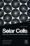
In Figure 2, an example result of the determination of optimal solar cell thickness as a function of light trapping (Z) is illustrated. In this analysis, the doping level was adjusted to yield a minority-carrier diffusion length twice the layer thickness, thus ensuring good collection efficiency. (We regarded this as a general design principle of thin silicon solar cells.) As a conservative estimate, the diffusion length for a given doping concentration was degraded by a factor of 5 from typical single-crystal values to account for the relatively inferior material quality generally expected for silicon deposited on a substrate. Modest surface passivation corresponding to front and back minority-carrier surface recombination velocities of 1000 cm/s, a front-surface solar-spectrum averaged reflection of 5%, and a series resistance of 0.1 ohm-cm were also assumed. The results of this analysis are shown in Figure 2 for a Z factor of 10. For this set of assumptions, the optimum efficiency occurs at silicon thicknesses between 30 and 40 microns.
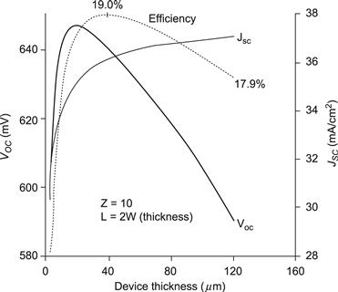
FIGURE 2 Thin silicon device performance predictions for the case where the optical thickness due to light trapping (Z) is 10 times the device thickness and the diffusion length is twice the actual device thickness. The optimum silicon thickness using these assumptions is in the range of 30–40 microns [8].
2.1 Methods of Implementing Light Trapping
As might be imagined, there is ample opportunity for creative designs to effect light trapping in silicon solar cells, and light-trapping structures have been realised by many different methods. For purposes of review, three types of reflective surfaces can be distinguished—random texture, geometric or regular structuring, and the use of optical elements external to the silicon solar cell structure.
2.1.1 Random Texturing
Random texturing holds promise for two reasons: modelling predicts that such random texturing can provide very reflective light trapping and the perceived ease at which random texture can be experimentally realised. For Lambertian diffuse reflectors made by random surface or interface texturing, and where the angular distribution of reflected light follows a cosine law, Goetzberger [5] has shown that the fraction of light reflected by total internal reflection at the front surface is equal to 1–1/n2, where n is the refractive index of silicon (approximately 3.4). In this case, when weakly absorbed light is reflected from a diffuse back reflector, 92% will be internally reflected from the front surface. The 50-fold increase in optical path length suggested by Yablonovitch and Cody [6] is based on front and back-surface texturing to effect Lambertian reflection. Unfortunately, the experimental realisation of a Lambertian reflector [9] has proved to be more difficult.
Random textures of varying effectiveness have been experimentally realised by the following methods:
2.1.2 Geometrical or Regular Structuring
Surface structuring is relatively easy to realise in single-crystal silicon wafer surfaces by taking advantage of the anisotropic (crystal orientation–dependent) etch rates of alkaline solutions. This approach has been used to fabricate the majority of light-trapping structures demonstrated to date, a few examples of which are shown in Figure 3. Common structures include 54-degree pyramids, inverted pyramids, slats, and perpendicular slats. Regular patterns are achieved with photolithography in combination with anisotropic etching [22–24]. Random pyramids are formed with the use of anisotropic etchants on nonpatterned surfaces [25,26], A similar result can be achieved in multicrystalline substrates (with much more effort) with the use of mechanical scribing, abrading or grinding, or laser ablation [27–32]. An option for very thin layers is conformal growth on a textured substrate [33] (Figure 3).

FIGURE 3 Examples of structured surfaces to effect light trapping in silicon solar cells [34].
Modelling of geometrical textures is often carried out by computer-aided ray-tracing techniques [35–38]. Ray-tracing analysis makes no assumptions about the distribution of light within the absorber layer. Instead, the path of representative incident rays of light are plotted using geometric optics to follow the light path through as it is reflected and refracted at surfaces and interfaces. Attenuation of light due to optical absorption in bulk silicon is also incorporated in the model. This approach is useful for the analysis of regularly structured surfaces [39] with complex geometries as well as unusual solar cell shapes such as the Spheral Solar™ Cell [40].
2.1.3 External Optical Elements
The solar cell can be overlayed with refractive optics elements such as prismatic cover slips (Figure 4) to effect a degree of light trapping. These optical elements were originally developed to ameliorate shading by the front contact grid metallisation, but they can also be used to redirect light back into the solar cell after it has escaped. External reflectors and optical cavities are two other examples of the use of external optical elements to implement light trapping. Miñiano et al. [41] have analysed light-confining cavities for concentrator solar cells.
FIGURE 4 A prismatic cover slip can be used to effect light trapping in solar cells [42].
2.2 Assessment of Light-Trapping Effects
Light trapping has been incorporated in structures with thickness ranging from less than 1 micron to 400 microns with varying degrees of success. The short-circuit current is the ultimate figure of merit for comparisons, as the objective of light trapping is to enhance absorption and contribute to minority-carrier generation. Using short-current current to assess the effectiveness of light-trapping schemes is complicated by other losses such as bulk recombination and front-surface reflection. In laboratory settings, spectral-response and reflection data can be analysed to extract detailed information about light trapping; however, these techniques require assumptions that limit their usefulness in predicting final cell performance. Each analysis method is reviewed in the following sections.
2.2.1 Short-Circuit Current Analysis of Light Trapping
Modelling the current generated by a known thickness of silicon is straightforward when all absorbed photons contribute a charge carrier. A ‘no light-trapping’ scenario can be generated that has perfect antireflection properties (no front-surface reflection) and only one pass of light through the device thickness (back surface is 100% absorbing with no contribution to current). To the extent an experimental result exceeds this model, light-trapping features are indicated. In real devices shading, imperfect AR, and parasitic absorption make the ‘no light-trapping’ model impossible to achieve [43]. Calibration of the light source is another source of error in this method.
Figure 5 shows modelling results and experimental data for short-circuit current as a function of thickness. The effect of light trapping becomes more pronounced as the device thickness is reduced and the light not absorbed on the first pass through the device grows to a significant level. Theoretical analysis of Green [44] and Tiedje [45] are included in Figure 5 and serve as the ‘best case’ limit for perfect light trapping. The analysis of Green appears to predict perfect collection (JSC = 44 mA/cm2) independently of thickness. The method of Tiedje assumes random texture, Lambertian-type reflection, and more realistic modelling using a loss-cone analysis for front-surface internal reflections. The baseline case with no light trapping was computed with PC-1D [46].

FIGURE 5 Summary of the last 5 years of published data on silicon-layer thickness and short-circuit current. Theoretical analyses are shown as lines. Laboratory results are shown as solid symbols [47–68].
The experimental results shown in Figure 5 indicate that most laboratory and commercial devices have not produced a level of photogenerated current exceeding that which would be possible in a device of comparable thickness without light trapping. Thus, based solely on total current, it cannot be concluded that in these particular solar cells light trapping makes a significant contribution to solar cell performance. These devices may include some light-trapping enhancement of current, but additional losses due to imperfect antireflection coatings, bulk and surface recombination, possibly exacerbated by adding light-trapping features to the solar cell, may have offset any gains from light trapping. This has prompted researchers to investigate other methods based on reflection and spectral-response measurement to analyse light-trapping effects in ways that are not obscured by various losses [69].
2.2.2 ‘Sub-Band-Gap’ Reflection Analysis of Light Trapping
The effectiveness of backside reflectors can be evaluated at long wavelengths (‘sub-band-gap’ energy photons)—i.e., longer than about 1100 nm. The silicon layer is approximately transparent to light in this wavelength range. As shown in the inset of Figure 6, the measured total reflection for nonabsorbed light at these wavelengths of a thin solar cell with a backside mirror is due to contributions of multiple internal reflections from the front and back surface. If absorption is negligible, then the ratio between the measured reflection and the reflection expected of an infinitely thick slab of silicon gives an estimate of the effective light trapping in a device. This technique does not measure light trapping per se but instead provides an indicator of the effectiveness of the backside mirror and the level of optical confinement for near-band-gap, weakly absorbed photons. This analysis can be especially decisive if test structures, both with and without backside reflectors, are compared. In thin silicon structures, the effect of the buried reflector is shown as an enhancement of sub-band-gap (>1050-nm-wavelength) reflection, which is attributed to unabsorbed light reflected at the backside mirror and transmitted through the front surface. This escaping light boosts the measured front-surface reflection (Figure 6), and the increased reflectance permits an estimate of the internal reflections in the silicon layer.
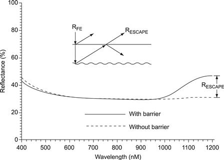
FIGURE 6 External reflection measurements in thin silicon structures with reflecting barrier layer between silicon layer and substrate [70].
2.2.3 Extended Spectral-Response Analysis of Light Trapping
The extended spectral-response method was developed by Basore [71] as a means to estimate an effective optical path length for near-band-gap light in a thin silicon solar cell, and it is based on an analysis of the internal quantum efficiency of a solar cell as a function of wavelength.
The method utilises a plot of 1/IQE versus 1/α, where α is the optical absorption coefficient for silicon and IQE is the internal quantum efficiency. Two representative examples of such plots are shown in Figure 7, for a thick silicon wafer-based solar cell and a thin (4 micron) silicon solar cell, both of which have textured surfaces to effect light trapping. The 1/IQE(λ) versus 1/α curves show two linear regions, which appears to be a general feature of solar cells with light trapping.
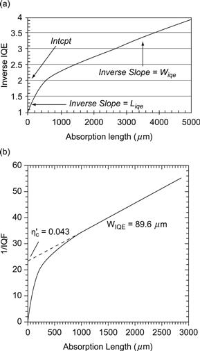
FIGURE 7 (a) Plot of 1/α vs. 1/IQE for a textured (thick) wafer-based silicon solar cell [71] and (b) textured 4-micron-thick silicon solar cell [72].
We will not discuss the details of the somewhat involved analysis in which Basore shows that the slopes and intercepts of the linearised parts of these curves can be used to estimate the collection efficiency, the back reflectance, the back-surface recombination velocity, and the effective minority-carrier diffusion length. This extended spectral-response analysis, although more complicated than other techniques, appears to be the most useful method for assessing light trapping in solar cells.
3 Voltage Enhancements in Thin Silicon Solar Cells
The factors that influence the open-circuit voltage of a silicon solar cell are the same whether the device is thin or thick. These include doping levels, the various bulk recombination mechanisms (defect-mediated Shockley–Read–Hall, radiative, and Auger), and surface recombination. The open-circuit voltage VOC depends logarithmically on the dark diode current density JO. The diode is analysed in terms of current components from the silicon layer (base) and a thin emitter layer formed on the surface of the base, usually by impurity diffusion. JO, can vary by orders of magnitude, depending on device parameters and silicon properties. The dark current can be calculated as
![]()
where q is the electronic charge, ni is the intrinsic carrier concentration of silicon; ND is the base doping concentration; S is the back-surface recombination velocity that characterises the extent of minority recombination at the silicon–substrate interface; L and D are the minority-carrier diffusion length and diffusivity in the base, respectively, and are sensitive to doping levels and material quality; and Wb is the thickness of the base. Actually, the above equation represents only the base layer contribution to JO. There is an analogous equation for emitter contribution to JO, but in well-designed solar cells, normally the base component is the dominant contribution to JO. At any rate, our purpose here is to simply highlight the factors that contribute to JO and indicate the design principles to reduce JO. In a thin silicon solar cell, the diffusion length will normally be longer than the layer thickness—i.e., Wb/L<1, in which case the above equation simplifies to
![]()
In such cases, the dark current does not depend on diffusion length but is directly proportional to the surface recombination velocity, thus underscoring the importance of surface passivation in thin silicon devices. Higher doping concentrations ND will decrease JO, so long as the doping does not degrade L such that L<W and bulk recombination becomes significant. Another consideration of high doping that is not evident from the above equations are band-gap narrowing effects. As doping levels exceed about 1019 atoms/cm3, the effective band gap of silicon is reduced, leading to increased intrinsic carrier concentrations ni, and correspondingly increased JO. Thus, increasing doping to increase VOC becomes self-defeating after a certain point.
3.1 Minority-Carrier Recombination Issues in Thin Silicon Solar Cells
As already pointed out, an important potential, although not completely experimentally verified, advantage of thin silicon solar cells is their decreased sensitivity to minority-carrier recombination. This permits higher doping levels to enhance open-circuit voltage and leads to better tolerance of impurities and defects. A sensitivity analysis of solar cell efficiency to device thickness and minority-carrier lifetime is shown in Figure 8. Minority-carrier lifetime τ and diffusion length L are related as
![]()
where D is the minority-carrier diffusivity, which is proportional to the minority-carrier mobility. While D is not highly sensitive to impurity and defects, τ can easily vary by more than an order of magnitude in silicon of various purity and quality. The analysis summarised in Figure 11 shows the interesting result that for a given minority-carrier lifetime there is an optimum thickness, and that for material with relative low minority-carrier lifetimes the optimum thickness is less than 50 microns.
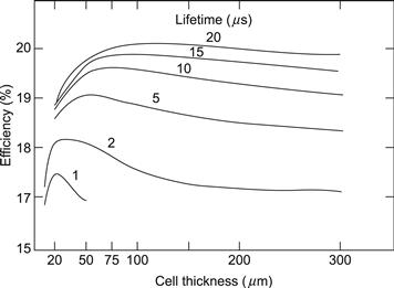
FIGURE 8 Sensitivity of solar cell efficiency to device thickness and minority-carrier lifetime [74].
Films of silicon deposited on substrates will usually be polycrystalline, although not all thin silicon solar cells are necessarily polycrystalline; epitaxial films removed from a monocrystalline silicon substrate and bonded to a superstrate, as well as solar cells made by thinning monocrystalline silicon wafers, need not have grain boundaries. In fact, these types of silicon solar cells provide an interesting control for exploring the effects of grain boundaries. Nevertheless, many low-cost approaches to thin silicon solar cells will produce material with varying grain sizes and textures. The effects of grain boundaries are complex and depend on the microstructure, film thickness, grain size distribution, junction depth, doping, etc. Diffused junctions can not only spike down grain boundaries, which may improve collection efficiency but also make the solar cell more prone to shunting effects (Figure 9). These issues are not unique to thin silicon solar cells, and, in fact, polycrystalline cast silicon solar cells have been an established line of solar cells for many years. Grain boundaries act as surfaces for minority-carrier recombination and can be depleted or accumulated and can exhibit space charge regions much as junctions and free surfaces. For single-crystal silicon solar cells, space-charge recombination is usually so small that it can be neglected, and the performance of the device, particularly open-circuit voltage, is controlled by bulk, surface, and shunt losses, but this may not be the case with multicrystalline solar cells. It was initially thought that polycrystalline silicon solar cells would suffer major short-circuit current and open-circuit voltage losses from grain-boundary recombination, which would severely restrict the maximum light-generated current [73]. However, it has been shown that when the grain diameter is several times larger than the intragrain (bulk) minority-carrier diffusion length, the short-circuit current is controlled not by grain-boundary recombination, but by the intragrain diffusion length.
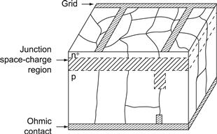
FIGURE 9 Geometry of grain boundaries in silicon solar cells [75].
Other factors that may play a substantial role in determining the electrical performance of polycrystalline silicon solar cells are the presence of inclusions and tunnel junctions, both of which act as resistive shunts and degrade the open-circuit voltage and fill factor locally. Although their impact on performance is fairly straightforward, it is not clear that either of these two possible defects is intrinsic to any polycrystalline silicon solar cell material or process. Accordingly, the analysis of the thin polycrystalline silicon solar cell is based on the relaxation of single crystal material and device properties due to the polycrystalline characteristics of the semiconductor.
As expected, increasing grain size results in better solar cell performance (Figure 10), but note the discontinuity between trends for p–i–n microcrystalline silicon solar cells and p–n multicrystalline silicon solar cells. The electric field in thin p–i–n cells is probably aiding collection efficiency and mediating the effect of grain-boundary recombination. The grain structure in these thin microcrystalline silicon solar cells may also have a texture resulting in grain boundaries with less electrical activity (e.g., minority-carrier recombination). Grain-boundary effects are one of the most active areas for research in silicon solar cells, and passivation techniques can be very effective in all types of multicrystalline silicon solar cells (Figure 11).

FIGURE 10 Effect of grain size on solar cell efficiency for p–i–n microcrystalline silicon devices and p–n multicrystalline thin silicon devices [76].
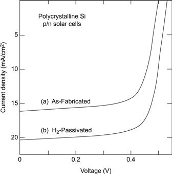
FIGURE 11 Hydrogen passivation of multicrystalline silicon solar cells showing improvement in current and voltage [77].
4 Silicon Deposition and Crystal Growth for Thin Solar Cells
In this section, we review some of the more important technologies used to realise thin silicon solar cells on supporting substrates (Figure 12). There is a wide range of methods used to deposit semiconductor materials, virtually all of which have been applied to some extent or degree to the production of thin silicon solar cells. This section is offered as a survey of the diverse approaches; space limitations do not permit an in-depth review. Where possible, common issues and criteria and unifying design principles are noted.
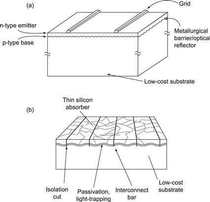
FIGURE 12 Generic polycrystalline thin-film-silicon device structures: (a) the electrically active part of the device consists of a thin silicon layer on top of a passive mechanically supporting substrate [78]; (b) similar structure with interconnection achieved monolithically, a benefit unavailable to conventional wafer-based devices [79].
4.1 Substrate Considerations
One of the key technological challenges to achieving a commercially viable thin-layer polycrystalline silicon solar cell technology is the development of a low-cost supporting substrate. The requirements for the substrate material are severe. Mechanical strength and thermal coefficient of expansion (TCE) matching are needed to prevent the film from breaking or deforming during handling and high-temperature processing. There are several good candidates for thermal expansion matched substrates, including mullite, a compound of alumina and silica. The substrate must also provide good wetting and nucleation during the film-growth process without contaminating the film. The substrate can be conducting or insulating, depending on device requirements. Finally, the substrate–silicon interface must provide a high degree of diffuse reflectivity and surface passivation.
The following substrates have been utilised to fabricate thin silicon solar cells:
4.2 High-Temperature Silicon-Deposition Methods
It is useful to distinguish silicon-deposition methods that employ high temperatures (>1000 °C) from low-temperature deposition techniques. The high temperatures impose significant constraints on and limit the choice of substrates, especially if a postdeposition recrystallisation step is desired. High-temperature deposition methods are probably the only way to achieve high silicon-deposition rates (e.g., 1–20 microns/min), and therefore, if silicon layers of 10–50-microns thickness are required, such high-temperature steps may be the only viable option. High-temperature deposition methods include
• Melt-growth or melt-coating techniques where elemental silicon is melted and then deposited as a film or layer on a substrate.
• Chemical vapour deposition (CVD) where a silicon-containing gaseous precursor is thermally decomposed on a substrate.
• Liquid-phase epitaxy (LPE) where silicon is precipitated from a molten metal solution.
4.2.1 Melt-Growth Techniques
Melt-growth processes characteristically have both high growth rates and good material quality [83,84,104]. An example melt-coating process is shown in Figure 13. In these examples, a substrate is contacted with molten silicon, which wets the substrate and then solidifies as a silicon layer. In many cases, the substrate is drawn through a bath of molten silicon. Generally, such processes cannot produce layers much less than 100 microns in thickness.

FIGURE 13 Honeywell silicon-on-ceramic dip-coating process [83].
4.2.2 Recrystallisation of Silicon
Related to melt growth are various recrystallisation techniques. These are generally not deposition processes per se but instead are used to melt already-deposited silicon layers and recrystallise them in order to achieve a more favourable grain structure. In this case, the grain structure of the as-deposited silicon layer is not critical, and the deposition process can be optimised for high-growth rates, large areas, and purity specifications. For instance, a plasma-enhanced CVD process such as shown in Figure 14 can be used to plate a silicon layer of desired thickness on a suitable substrate, such as a ceramic, which is compatible with a recrystallisation step.
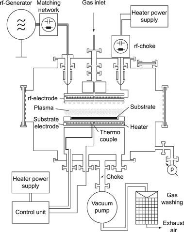
FIGURE 14 PECVD silicon-deposition process [105].
In the preferred techniques of recrystallisation, the deposited silicon layer is not usually simultaneously melted in its entirety. Instead, a zone-melting recrystallisation (ZMR) process is effected by localised heating to create a melted zone that moves or scans across the deposited silicon layer, melting the silicon at the leading edge and resolidifying a silicon layer at the trailing edge. Such ZMR techniques can yield millimetre- to centimetre-sized grain structures. There are several ways to induce localised or zone melting of layers, including moving point- or line-focused infrared lamps, travelling resistively heated strip heaters, and laser and electron beams. Figure 15 shows several of these ZMR techniques commonly used for silicon solar cell applications.
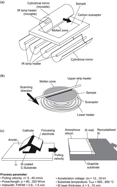
FIGURE 15 (a) Halogen IR lamp heating for ZMR [106]. (b) Travelling strip heaters for ZMR [107]. (c) Electron beam heating [108].
Much work has been done on optimising the quality of silicon layers produced by ZMR. For example, Figure 16 shows the effects of silicon layer thickness and zone-melting scan speed on the defect density of recrystallised silicon layers.
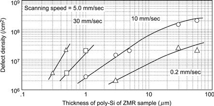
FIGURE 16 Relation between deposited-silicon-layer thickness, scan speed, and silicon-defect density in ZMR [109].
4.2.3 High-Temperature Silicon Chemical Vapour Deposition
Chemical vapour deposition or CVD is defined as the formation of a solid film on a substrate by reacting vapour-phase chemicals, or ‘precursors,’ that contain the desired constituents [110]. For example, substrates can be coated with silicon layers by decomposition of gaseous silane (SiH4) or trichlorosilane (SiHCl3). In fact, many precursors are possible for silicon CVD, and silane or the chlorosilanes are probably the most commonly used—although, for example, iodine and bromine compounds are also sometimes considered as silicon precursors. In general, silicon CVD is a well-developed technology commonly used in integrated circuit fabrication, in which case it is often used for epitaxial growth of silicon layers on monocrystalline silicon substrates. For solar cell applications where CVD is used to deposit a 10- to 50-micron-thick silicon layer for subsequent, postdeposition ZMR, the CVD is optimised for high-precursor utilisation (i.e., the fraction of precursor converted to silicon), deposition efficiency (i.e., the fraction of deposited silicon that ends up on the substrate rather than the walls of the reactor chamber or the substrate susceptor), the deposition rate, the purity of the deposited silicon, areal uniformity, the potential to recover unreacted precursors or reaction product, and various safety and environmental issues.
For solar cell applications, three types of CVD are most used:
In all these types of CVD, a gaseous silicon precursor (e.g., SiH4 or SiHCl3), generally mixed with a dilution carrier gas such as hydrogen or nitrogen, is delivered into a reaction chamber. These gases move from the inlet to the outlet in a continuous stream to form the main gas-flow region that brings the precursor into close proximity of the heated substrate. Some further description and details of the three main types of CVD processes used for thin silicon solar cells follows.
Atmospheric Pressure CVD
APCVD systems were historically the first used for applications in the microelectronics industry [111,112]. These systems are simple in design and are generally composed of three subsystems: a gas delivery system, a reactor, and an effluent-abatement system. For the most part, APCVD is carried out at relatively high temperatures for silicon-containing precursors (1100–1250 °C). This allows for high deposition rates to be achieved. At these high temperatures, APCVD is in the mass-transport limited regime. This requires that a very uniform gas flow be achieved within the reactor to ensure that all areas of the heated substrate are exposed to equal amounts of precursor. This requirement is the primary concern during APCVD reactor geometry design and, to date, has limited this process to batch-type processes with respect to CVD silicon.
Rapid Thermal CVD
RTCVD is a variation of APCVD. It is based on the energy transfer between a radiant heat source and an object with very short processing times—seconds or minutes. This is typically from an optical heating system such as tungsten halogen lamps. The obvious benefit of this process is the fast cycle times for heating substrates to their required deposition temperature. A detailed explanation of this process along with its advantages and disadvantages can be found in Faller et al. [113].
Low-pressure CVD
LPCVD systems are inherently more complex than APCVD systems since they require robust vacuum systems that are capable of handling the often toxic corrosive precursor effluents. With respect to silicon deposition, LPCVD is generally conducted using vacuum pressures of 0.25–2.0 torr and temperatures of 550–700 °C. At these pressures and temperatures LPCVD is in the surface rate-limited regime. It is important to note that at reduced pressures the diffusivity of the precursor is greatly enhanced. This allows for multiple wafers to be stacked very closely together, on the order of a few millimetres, and still achieve a highly uniform deposition. However, in order to ensure this, very precise temperature control is necessary across the entire reactor, within 0.5–l°C is not uncommon. Since LPCVD is in the surface rate-limited regime it has the constraint of very low deposition rates. These low growth rates have limited its application in silicon solar cell fabrication.
A summary of silicon CVD growth rates for various precursors and deposition temperatures is given in Table 1.
TABLE 1 Common Silicon Precursors
| Silicon precursor | Deposition temperature (°C) | Growth rales (μm/min) |
| Silicon tetrachloride (SiCl4) | 1150–1250 | 0.4–1.5 |
| Trichlorosilane (SiCl3H) | 1000–1150 | 0.4–4.0 |
| Dichlorosilane (SiH2Cl2) | 1020–1120 | 0.4–3.0 |
| Silane (SiH4) | 650–900 | 0.2–0.3 |
| Disilane (Si2H6) | 400–600 | <0.1 |
4.2.4 Low-Temperature Chemical Vapour Deposition
Some low-temperature chemical vapour techniques can be distinguished from the high-temperature (>1000 °C) CVD processes discussed previously. These methods are employed with substrates such as glass that are not compatible with either a high-temperature deposition step or a postdeposition recrystallisation step. The relatively slow growth rates inherent in a low-temperature deposition process necessitates thin device structures on the order of several microns thickness or less. The as-deposited silicon layers have average grain sizes of 1 micron or less and are characterised as microcrystalline. Hydrogenated microcrystalline silicon solar cells using a p–i–n structure, which is similar to the amorphous silicon solar cell structure, can achieve very respectable conversion efficiencies in excess of 10%. The benefits of such microcrystalline silicon solar cells over amorphous silicon solar cells are a greater stability to light-induced degradation processes. The deposition processes for microcrystalline silicon solar cells are typically adaptations of those used for amorphous silicon solar cells.
Liquid-phase Epitaxy (LPE)
Liquid-phase epitaxy is a metallic solution growth technique that can be used to grow semiconductor layers on substrates. Silicon can be precipitated from solutions of a number of molten metals in the temperature range 600–1200 °C. This method has been used to grow thin silicon solar cells on low-cost metallurgical grade (MG) silicon substrates. In this case, the MG silicon substrate is too impure for direct use in photovoltaics. Instead, the substrate is used as a substrate for the growth of high-purity layers of silicon by either LPE or CVD. The MG silicon provides a thermal-expansion matched substrate for the thin silicon solar cell. The grain size of MG substrates is relatively large (several millimetres to centimetres in lateral dimension); as the epitaxial layer will replicate the grain structure of the silicon substrate, this approach will yield thin silicon solar cells with large grain sizes. One issue with using a MG silicon substrate is contamination of the solar cell device by outdiffusing substrate impurities. Other favourable features of LPE are the high mobility of adatoms in the liquid phase (as compared to surface diffusion upon which vapour-phase techniques depend) and the near-equilibrium growth conditions that reduce point defects and dislocations originating from the substrate. A conventional slideboat LPE system, similar to that used for making compound semiconductor optoelectronics devices and suitable for R&D of LPE thin silicon solar cells, is shown in Figure 17. This type of LPE system employs a programmed transient cooling mode and is essentially a batch process. Steady-state LPE processes (Figure 18) using an imposed temperature difference across the growth solution in conjunction with a solid silicon source to replenish the solution have been proposed and developed for high-throughput production.
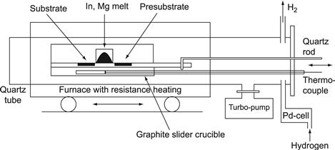
FIGURE 17 Small-scale LPE system [114].

FIGURE 18 Principle of the temperature-difference method [115].
5 Thin Silicon Solar Cells Based on Substrate Thinning
Figure 19 shows a solar cell made by thinning and grooving the backside of a silicon wafer. Such solar cells obviously have little cost advantage in that they utilise a high-quality silicon wafer and add considerable processing complexity. Because of the decreased sensitivity of performance to lifetime in such thin solar cells, they have application to space solar cells due to their potential radiation hardness. Further, these cells provide a means of studying basic effects such as light trapping and surface passivation in thin solar cell structures without the complicating issues of material quality and grain boundaries. A similar type of thin solar cell is shown in Figure 20. This device structure permits a planar back mirror to be effected close to the front surface (Figure 20(a)). The dependence of short-circuit current on effective device thickness can be readily studied with this type of thin solar cell (Figure 20(b)).
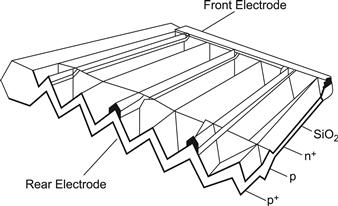
FIGURE 19 Thinned and grooved wafer-based silicon solar cell [116].

FIGURE 20 (a) Cross-section of ultra-thin, self-supporting MIS solar cell made by structuring a silicon wafer [117]. (b) Short-circuit current as a function of active-layer silicon thickness for solar cell structures shown in inset [117].
Even thinner silicon solar cells can be made with silicon wafers using epitaxial growth, provided a superstrate is used for mechanical support. For instance, Figure 21 shows a thin silicon solar cell made by layer transfer and wafer-bonding techniques. An epitaxial silicon solar cell structure is grown on a monocrystalline silicon substrate. The structure is then bonded to a glass superstrate. The silicon substrate is then removed. Most simply, the removal of the silicon substrate can be effected by controlled etching, in which case the substrate is dissolved away. Various schemes have been proposed to separate the substrate from the epitaxial layer after bonding the solar cell structure to a superstrate. One method of achieving this shown in detail in Figure 22. Some creative variations on this approach have been reported; for example, see Figure 23.
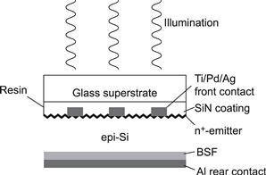
FIGURE 21 Monocrystalline silicon substrate made by layer transfer and bonding to a glass superstrate [119].

FIGURE 22 Schematic representation of series connection of thin-film Si-transfer solar cells. (a) Two epitaxial thin-film silicon solar cells connected to the host wafer with the separation layer (columns). A metal stripe (Ag) is soldered to the front-side grid of the left solar cell. Mesa grooves provide electrically isolation of the emitter in the interconnection area. (b) Epoxy resin fixes the superstrate glass to the surface of the cell. (c) Mechanical force removes the host wafer from the cell. (d) A groove structured via chip dicing sawing separates the two solar cells. Oblique deposition of aluminium creates the back contact of the solar cells and electrically connects the metal stripe that is in contact with the front side grid of the left solar cell with the back-side contact of the right solar cell [120].
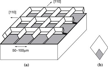
FIGURE 23 An example of the epitaxial lift-off process [121].
6 Summary of Device Results
We end this review by summarising results for thin silicon solar cells. Table 2 lists reports for thin silicon layers made by high-temperature growth methods, often including a postdeposition recrystallisation (e.g., ZMR) step, on nonsilicon substrates such as ceramics, graphite, and high-temperature glasses. Samples are characterised either by diffusion length or minority-carrier lifetime or, in cases where a solar cell was made, by efficiency. Table 3 shows a similar summary of results for thin silicon solar cell structures on silicon-based substrates, which include oxidised silicon, MG silicon, and various types of silicon sheet.
TABLE 2 High-Temperature Growth on Foreign Substrates
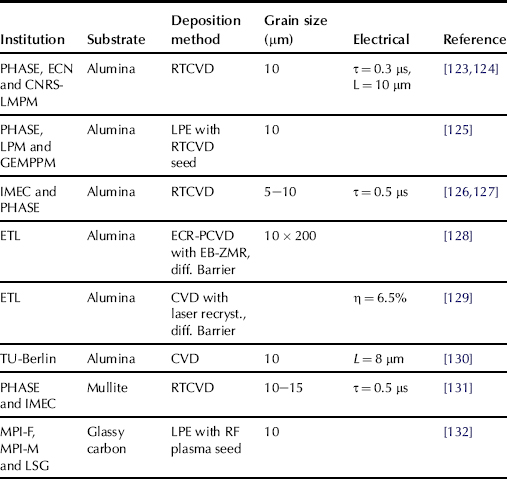
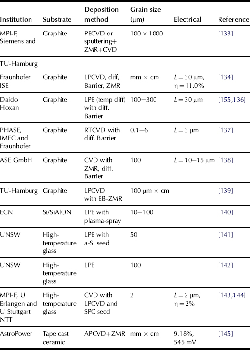
(after Catchpole et al. [122])
TABLE 3 Summary of Thin Silicon-On-Silicon Device Results
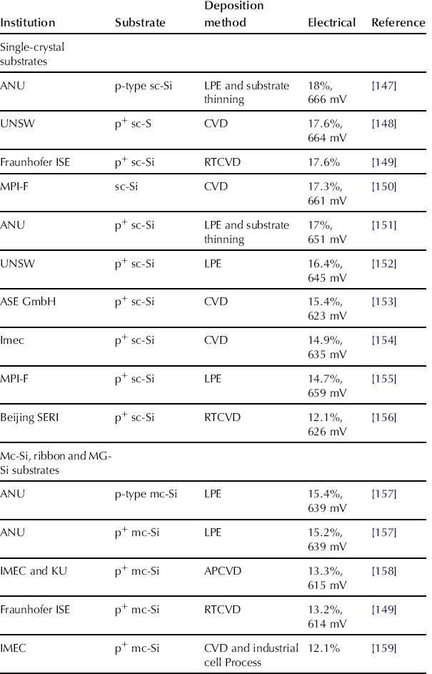
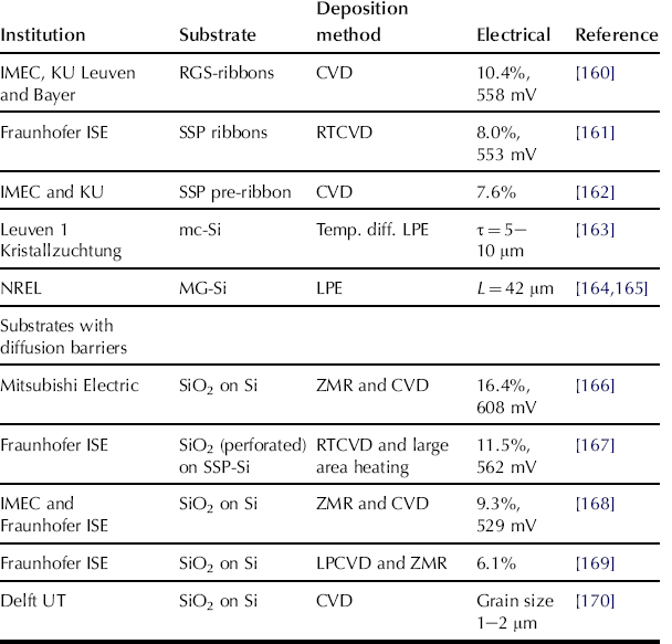
(after McCann et al. [146])
References
1. Redfield D. Enhanced photovoltaic performance of thin silicon films by multiple light passes. Scottsdale: Proceedings of the 11th IEEE Photovoltaic Specialists Conference; 1975; pp. 431–432.
2. Spitzer M, Shewchun J, Vera ES, Loferski JJ. ultra high efficiency thin silicon p–n junction solar cells using reflecting surfaces. San Diego: Proceedings of the 14th IEEE Photovoltaic Specialists Conference; 1980; pp. 375–380.
3. Barnett AM. thin film solar cell comparison methodology. San Diego: Proceedings of the 14th IEEE Photovoltaic Specialists Conference; 1980; pp. 273–280.
4. Werner JH, Bergmann RB. Crystalline silicon thin film solar cells. Jeju: Technical Digest International PVSEC-12; 2001; pp. 69–72.
5. Goetzberger A. Optical confinement in thin si-solar cells by diffuse back reflectors. Orlando: Proceedings of the 15th IEEE Photovoltaic Specialists Conference; 1981; pp. 867–870.
6. Yablonovitch E, Cody GD. Intensity enhancement in textured optical sheets for solar cells, IEEE Trans. Electron Devices ED-29 1982;:300–305.
7. D. Redfield, Thin-film silicon solar cell multiple-pass. Appl. Phys. Lett. 25(11), 647– 648.
8. Barnett AM, Rand JA, Domian FA, et al. Efficient thin silicon-film solar cells on low cost substrates. Florence, Italy: Proceedings of the 8th European Photovoltaic Solar Energy Conference; 1988; pp. 149–155.
9. Green MA, Campbell P. Light trapping properties of pyramidally textured and grooved surfaces. New Orleans: Proceedings of the 9th IEEE Photovoltaic Specialists Conference; 1987; pp. 912–917.
10. Ruby DS, Yang P, Zaidi S, et al. Improved performance of self-aligned, selective- emitter silicon solar cells. Vienna: Proceedings of the 2nd World Conference on Photovoltaic Solar Energy Conversion; 1988; pp. 1460–1463.
11. Schnell M, Lüdemann R, Schaefer S. Plasma surface texturization for multicrystalline silicon solar cells. Anchorage: Proceedings of 28th IEEE Photovoltaic Specialists Conference; 2000; pp. 367–370.
12. Wells T, El-Gomati MM, Wood J. Low temperature reactive ion etching of silicon with SF6/O2 plasmas. J Vac Sci Technol B. 1997;15:397.
13. Deckman HW, Roxlo CB, Wronski CR, Yablonovitch E. Optical enhancement of solar cells. Proceedings of the 17th IEEE Photovoltaic Specialists Conference 1984;955–960.
14. Stocks MJ, Carr AJ, Blakers AW. Texturing of polycrystalline silicon. Hawaii: Proceedings of the 24th IEEE Photovoltaic Specialists Conference; 1994; pp. 1551–1554.
15. Deckman HW, Wronski CR, Witzke H, Yablonovitch E. Optically enhanced amorphous solar cells. Appl Phys Lett. 1983;42(11):968–970.
16. Tsuo YS, Xiao Y, Heben MJ, Wu X, Pern FJ, Deb SK. potential applications of porous silicon in photovoltaics. Louisville: Proceedings of the 23rd IEEE Photovoltaic Specialists Conference; 1993; pp. 287–293.
17. Cudzinovic M, Sopori B. Control of back surface reflectance from aluminum alloyed contacts on silicon solar cells. Washington DC: Proceedings of the 25th IEEE Photovoltaic Specialists Conference; 1996; pp. 501–503.
18. Rothwarf A. Enhanced solar cell performance by front surface light scattering. Las Vegas: Proceedings of the 18th IEEE Photovoltaic Specialists Conference; 1985; pp. 809–812.
19. Gee JM, King RR, Mitchell KW. High-efficiency cell structures and processes applied to photovoltaic-grade czochralski silicon. Washington DC: Proceedings of the 25th IEEE Photovoltaic Specialists Conference; 1996; pp. 409–412.
20. Gee JM, Gordon R, Liang H. Optimization of textured-dielectric coatings for crystalline-silicon solar cells. Washington DC: Proceedings of the 25th IEEE Photovoltaic Specialists Conference; 1996; pp. 733–736.
21. Hegedus SS, Deng X. Analysis of optical enhancement in a-si n–i–p solar cells using a detachable back reflector. Washington DC: Proceedings of the 25th IEEE Photovoltaic Specialists Conference; 1996; pp. 1061–1064.
22. Tobin SP, Keavney CJ, Geoffroy LM, Sanfacon MM. Experimental comparison of light-trapping structures for silicon solar cells. Las Vegas: Proceedings of the 20th IEEE Photovoltaic Specialists Conference; 1988; pp. 545–548.
23. Rand JA, Hall RB, Barnett AM. light trapping in thin crystalline silicon solar cells. Orlando: Proceedings of the 21st IEEE Photovoltaic Specialists Conference; 1990; pp. 263–268.
24. Restrepo F, Backus CE. IEEE Trans. Electron Devices. 1976;23:1195–1197.
25. Campbell P, Wenham SR, Green MA. Light-trapping and reflection control with tilted Pyramids and Grooves. Las Vegas: Proceedings of the 20th IEEE Photovoltaic Specialists Conference; 1988; pp. 713–716.
26. King DL, Buck ME. Experimental optimization of an anisotropic etching process for random texturization of silicon solar cells. Las Vegas: Proceedings of the 22nd IEEE Photovoltaic Specialists Conference; 1991; pp. 303–308.
27. Terheiden B, Fath P, Bucher E. The MECOR (mechanically corrugated) silicon solar cell concept. Anchorage: Proceedings of the 28th IEEE Photovoltaic Specialists Conference; 2000; pp. 399–402.
28. Fath P, et al. Multicrystalline silicon solar cells using a new high-throughput mechanical texturization technology and a roller printing metallization technique. Nice: Proceedings of the 13th European Photovoltaic Solar Energy Conference; 1995; pp. 29–32.
29. Narayanan S, Wenham SR, Green MA. Sydney: Technical Digest International PVSEC-4; 1989; p. 1111.
30. Kaiser U, Kaiser M, Schindler R. Texture etching of multicrystalline silicon. Lisbon: Proceedings of the 10th European Photovoltaic Solar Energy Conference; 1991; pp. 293–294.
31. Willeke G, Nussbaumer H, Bender H, Bucher E. Mechanical texturization of multicrystalline silicon using a conventional dicing saw and bevelled blades. Montreux: Proceedings of the 11th European Photovoltaic Solar Energy Conference; 1992; pp. 480–483.
32. Stocks MJ, Carr JJ, Blakers AW. Texturing of polycrystalline silicon. Hawaii: Proceedings of the First World Conference on Photovoltaic Energy Conversion; 1994; pp. 1551–1554.
33. Campbell P, Keevers M. Light trapping and reflection control for silicon thin films deposited on glass substrates textured by embossing. Anchorage: Proceedings of the 28th IEEE Photovoltaic Specialists Conference; 2000; pp. 355–358.
34. Thorp D, Campbell P, Wenham SR. Absorption enhancement in conformally textured thin-film silicon solar cells. Washington DC: Proceedings of the 25th IEEE Photovoltaic Specialists Conference; 1996; pp. 705–708.
35. Smith AW, Rohatgi A, Neel SC. Texture: A ray-tracing program for the photovoltaic community. Orlando: Proceedings of the 21st IEEE Photovoltaic Specialists Conference; 1990; pp. 426–431.
36. Sopori BL, Marshall T. Optical confinement in thin silicon films: a comprehensive ray optical theory. Louisville: Proceedings of the 23rd IEEE Photovoltaic Specialists Conference; 1993; pp. 127–132.
37. Rau U, Meyer T, Goldbach M, Brendel R, Werner JH. Numerical simulation of innovative device structures for silicon thin-film solar cells. Washington DC: Proceedings of the 25th IEEE Photovoltaic Specialists Conference; 1996; pp. 469–472.
38. Abouelsaood AA, Ghannam MY, Poortmans J, Mertens RP. Accurate modeling of light trapping in thin film silicon solar cells. Proceedings of the Twenty-sixth IEEE Photovoltaic Specialists Conference 1997; pp. 183–186.
39. Campbell P, Green MA. light trapping properties of pyramidally textured surfaces. J Appl Physics July 1987;243–249.
40. Bisconti R, Ossenbrink HA. Light trapping in spheral solart cells. Nice: Proceedings of the 13th European Photovoltaic Solar Energy Conference; 1995; pp. 386–389.
41. Minano JC, Luque A, Tobias I. Light-confining cavities for photovoltaic applications based on the angular-spatial limitation of the escaping beam. Appl Opt. 1992;31(16):3114–3122.
42. Zhao J, Wang A, Blakers AW, Green MA. High efficiency prismatic cover silicon concentrator solar cells. Las Vegas: Proceedings of the 20th IEEE Photovoltaic Specialists Conference; 1988; pp. 529–531.
43. Gee JM. The effect of parasitic absorption losses on light trapping in thin silicon solar cells. Las Vegas: Proceedings of the 20th IEEE Photovoltaic Specialists Conference; 1988; pp. 549–554.
44. Green MA, et al. Enhanced light-trapping in 21.5% efficient thin silicon solar cells. Nice: Proceedings of the 13th European Photovoltaic Solar Energy Conference; 1995; pp. 13–16.
45. Tiedje T, Yablonovitch E, Cody GD, Brooks BG. Limiting efficiency of silicon solar cells. IEEE Trans Electron Devices ED-31 1984;711–716.
46. Basore PA. Numerical modeling of textured silicon solar cells using PC-ID, ZEEE. Trans Electron Devices ED-37 1990;337.
47. Zimmerman W, Eyer A. Coarse-grained crystalline silicon thin film solar cells on laser perforated SIO2 Barrier Layers. Anchorage: Proceedings of the 28th IEEE Photovoltaic Specialists Conference; 2000; pp. 233–236.
48. Bruton TM, Roberts S, Heasman KC, Russell R. Prospects for high efficiency silicon solar cells in thin czochralski wafers using industrial processes. Anchorage: Proceedings of the 28th IEEE Photovoltaic Specialists Conference; 2000; pp. 180– 183.
49. Berge C, Bergmann RB, Rinke TJ, Werner JH. Monocrystalline silicon thin film solar cells by layer transfer. Munich: Seventeenth European Photovoltaic Solar Energy Conference; 2001; pp. 1277–1281.
50. Zimmerman W, Bau S, Eyer A, Haas F, Oßwald D. Crystalline silicon thin film solar cells on low quality silicon substrates with and without SiO2 intermediate layer. Glasgow: Proceedings of the 16th European Photovoltaic Solar Energy Conference; 2000; pp. 1144–1147.
51. Finck von Finckenstein B, Horst H, Spiegel M, Fath P, Bucher E. Thin MC SI low cost solar cells with 15% efficiency. Anchorage: Proceedings of the 28th IEEE Photovoltaic Specialists Conference; 2000; pp. 198–200.
52. Zahedi C, Ferrazza F, Eyer A, et al. Thin film silicon solar cells on low-cost metallurgical silicon substrates by liquid phase epitaxy. Glasgow: Proceedings of the 16th European Photovoltaic Solar Energy Conference; 2000; pp. 1381–1384.
53. Tanda M, Wada T, Yamamoto H, Isomura M, Kondo M, Matsuda A. Key technology for mc-Si thin-film solar cells prepared at a high deposition rate. Sapporo: Technical Digest International PVSEC-11; 1999; pp. 237–238.
54. Hanoka JI. An overview of silicon ribbon-growth technology. Sapporo: Technical Digest International PVSEC-11; 1999; pp. 533–534.
55. Brendel R, Auer R, Feldrapp K, et al. Crystalline thin-film si cells from layer transfer using Porous Si (PSI-Process). New Orleans: Proceedings of the 29th IEEE Photovoltaic Specialists Conference; 2002; pp. 86–89.
56. Meier DL, Jessup JA, Hacke Jr P, Granata SJ. production of thin (70–100 mm) crystalline silicon cells for conformable modules. New Orleans: Proceedings of the 29th IEEE Photovoltaic Specialists Conference; 2002; pp. 110–113.
57. Cudzinovic MJ, McIntosh KR. Process simplifications to the pegasus solar cell— sunpower’s high-efficiency bifacial silicon solar cell. New Orleans: Proceedings of the 29th IEEE Photovoltaic Specialists Conference; 2002; pp. 70–73.
58. Schmidt J, Oberbeck L, Rinke TJ, Berge C, Bergmann RB. Application of plasma silicon nitride to crystalline thin-film silicon solar cells. Munich: Proceedings of the 17th European Photovoltaic Solar Energy Conference; 2001; pp. 1351– 1354.
59. Münzer KA, Eisenrith KH, Schlosser RE, Winstel MG. 18% PEBSCO— Silicon solar cells for manufacturing. Munich: Proceedings of the 17th European Photovoltaic Solar Energy Conference; 2001; pp. 1363–1366.
60. Tayanaka H, Nagasawa A, Hiroshimaya N, Sato K, Haraguchi Y, Matsushita T. Effects of crystal defects in single-crystalline silicon thin-film solar cell. Munich: Proceedings of the 17th European Photovoltaic Solar Energy Conference; 2001; pp. 1400–1403.
61. Terheiden B, Fischer B, Fath P, Bucher E. Highly efficient mechanically V-textured silicon solar cells applying a novel shallow angle contacting scheme. Munich: Proceedings of the 17th European Photovoltaic Solar Energy Conference; 2001; pp. 1331–1334.
62. Schneiderlöchner E, Preu R, Lüodemann R, Glunz SW, Willeke G. Laser-fired contacts. Munich: Proceedings of the 17th European Photovoltaic Solar Energy Conference; 2001; pp. 1303–1306.
63. Glunz SW, Dicker J, Kray D, et al. High efficiency cell structures for medium-quality silicon. Munich: Proceedings of the 17th European Photovoltaic Solar Energy Conference; 2001; pp. 1286–1292.
64. Yamamoto K, Yoshimi M, Suzuki T, Okamoto Y, Tawada Y, Nakajima A. Thin film poly-si solar cell with star structure on glass substrate fabricated at low temperature. Anaheim: Proceedings of the Twenty-sixth IEEE Photovoltaic Specialists Conference; 1997; pp. 575–580.
65. Yamamoto K, Yoshimi M, Tawada Y, Okamoto Y, Nakajima A. Cost effective and high performance thin film si solar cell towards the twenty-first century. Sapporo: Technical Digest International PVSEC-11; 1999; pp. 225–228.
66. Golay S, Meier J, Dubail S, Fay S, Kroll U, Shah A. First pin/pin micromorph modules by laser patterning. Anchorage: Proceedings of the 28th IEEE Photovoltaic Specialists Conference; 2000; pp. 1456–1459.
67. Meier J, Vallat-Sauvain E, Dubail S, et al. Microcrystalline silicon thin-film solar cells by the VHF-GD technique. Sapporo: Technical Digest International PVSEC-11; 1999; pp. 221–223.
68. Shah A, Meier J, Torres P, et al. Recent progress on microcrystalline solar cells. Anaheim: Proceedings of the 26th IEEE Photovoltaic Specialists Conference; 1997; pp. 569–574.
69. Rand JA, Basore PA. Light-trapping silicon solar cells experimental results and analysis. Las Vegas: Proceedings of the 22nd IEEE Photovoltaic Specialists Conference; 1991; pp. 192–197.
70. Rand JA, Ford DH, Bacon C, et al. Silicon-film product II: initial light trapping results. Lisbon: Proceedings of the 10th European Photovoltaic Solar Energy Conference; 1991; pp. 306–309.
71. Basore PA. Extended spectral analysis of internal quantum efficiency. Louisville: Proceedings of the 23rd IEEE Photovoltaic Specialists Conference; 1993; pp. 147–152.
72. Yamamoto K, Suzuki T, Yoshimi M, Nakajima A. Low temperature fabrication of thin film polycrystalline si solar cell on the glass substrate and its application to the a-Si:h/polycrystalline Si tandem solar cell. Washington DC: Proceedings of the 25th IEEE Photovoltaic Specialists Conference; 1996; pp. 661–664.
73. Rothwarf A. Crystallite size considerations in polycrystalline solar cells. Baton Rouge: Proceedings of the 12th IEEE Photovoltaic Specialists Conference; 1976; pp. 488–495.
74. Mokashi AR, Daud T, Kachare AH. Simulation analysis of a novel high efficiency silicon solar cell. Las Vegas: Proceedings of the 18th IEEE Photovoltaic Specialists Conference; 1985; pp. 573–577.
75. Milstein JB, Tsuo YS, Hardy RW, Surek T. The influence of grain boundaries on solar cell performance. Orlando: Proceedings of the 15th IEEE Photovoltaic Specialists Conference; 1981; pp. 1399–1404.
76. Beaucarne G, Bourdais S, Slaoui A, Poortmans J. Carrier collection in fine- grained p–n junction polysilicon solar cells. Anchorage: Proceedings of the 28th IEEE Photovoltaic Specialists Conference; 2000; pp. 128–133.
77. Kazmerski LL. Silicon grain boundaries: correlated chemical and electro-optical characterization. Orlando: Proceedings of the 17th IEEE Photovoltaic Specialists Conference; 1984; pp. 379–385.
78. Barnett AM, Rand JA, Domian FA, et al. Efficient thin silicon-film solar cells on low-cost substrate. Florence: Proceedings of the 8th European Photovoltaic Energy Conference; 1988; pp. 149–155.
79. Ford DH, Rand JA, Barnett AM, DelleDonne EJ, Ingram AE, Hall RB. Development of light-trapped, interconnected, silicon-film modules. Anaheim: Proceedings of the 26th IEEE Photovoltaic Specialists Conference; 1997; pp. 631–634.
80. Silier M, Konuma A, Gutjahr E, et al. High-quality polycrystalline silicon layers grown on dissimilar substrates from metallic solution. Washington, DC: I. Proceedings of the 25th IEEE Photovoltaic Specialists Conference; 1996; pp. 681–684.
81. Bergmann R, Kühnle J, Werner JH, et al. Polycrystalline silicon for thin film solar cells. Hawaii: Proceedings of the 24th IEEE Photovoltaic Specialists Conference; 1994; pp. 1398–1401.
82. Andrä G, Bergmann J, Ose E, Schmidt M, Sinh ND, Falk F. Multicrystalline LLC-Silicon thin film cells on glass. New Orleans: Proceedings of the 29th IEEE Photovoltaic Specialists Conference; 2002; pp. 1306–1309.
83. Zook JD, Shuldt SB, Maciolek RB, Heaps JD. Growth, evaluation and modeling of silicon-on-ceramic solar cells. Washington DC: Proceedings of the 13th IEEE Photovoltaic Specialists Conference; 1978; pp. 472–478.
84. Heaps JD, Schuldt SB, Grung BL, Zook JD, Butter CD. Continuous coating of silicon-on-ceramic. San Diego: Proceedings of the 14th IEEE Photovoltaic Specialists Conference; 1980; pp. 39–48.
85. Minagawa S, Saitoh T, Warabisako T, Nakamura N, Itoh H, Tokuyama T. Fabrication and characterization of solar cells using dendritic silicon thin films grown on alumina ceramic. Baton Rouge: Proceedings of the 12th IEEE Photovoltaic Specialists Conference; 1976; pp. 77–81.
86. Barnett AM, Fardig DA, Hall RB, Rand JA, Ford DH. Development of thin silicon-film solar cells on low-cost substrates. New Orleans: Proceedings of the 9th IEEE Photovoltaics Specialists Conference; 1987; pp. 1266–1270.
87. van Roosmalen JAM, Tool CJJ, Huiberts RC, Beenen RJG, Huijsmans JPP, Sinke WC. Ceramic substrates for thin-film crystalline silicon solar cells. Washington DC: Proceedings of the 25th IEEE Photovoltaic Specialists Conference; 1996; pp. 657–660.
88. Shuldt SB, Heaps JD, Schmit FM, Zook JD, Grung BL. Large area silicon- on-ceramic substrates for low cost solar cells. Orlando: Proceedings of the 15th IEEE Photovoltaic Specialists Conference; 1981; pp. 934–940.
89. Slaoui A, Rusu M, Fosca A, Torrecillas R, Alvarez E, Gutjar A. Investigation of barrier layers on ceramics for silicon thin film solar cells. New Orleans: Proceedings of the 29th IEEE Photovoltaic Specialists Conference; 2002; pp. 90–93.
90. DelleDonne E, Ingram A, Jonczyk R, et al. Thin silicon-on-ceramic solar cells. New Orleans: Proceedings of the 29th IEEE Photovoltaic Specialists Conference; 2002; pp. 82–85.
91. Barnett AM, Mauk MG, Zolper JC, Hall RB, McNeely JB. Thin-film silicon and gaAs solar cells on metal and glass substrates. Kobe: Technical Digest International PVSEC-1; 1984; pp. 241–244.
92. Barnett AM, Mauk MG, Hall RB, Fardig DA, McNeely JB. Design and development of efficient thin-film crystalline silicon solar cells on steel substrates. London: Proceedings of the 6th European Photovoltaic Solar Energy Conference; 1985; pp. 866–870.
93. Barnett AM, Hall RB, Fardig DA, Culik JS. Silicon-film solar cells on steel substrates. Las Vegas: Proceedings of the 18th IEEE Photovoltaics Specialists Conference; 1985; pp. 1094–1099.
94. Kunze T, Hauttmann S, Seekamp J, Müller J. Recrystallized and epitaxially thickened poly-silicon layers on graphite substrates. Anaheim: Proceedings of the 26th IEEE Photovoltaic Specialists Conference; 1997; pp. 735–738.
95. Chu TL, Mollenkopf HC, Singh KN, Chu SS, Wu IC. Polycrystalline silicon solar cells for terrestrial applications. Scottsdale: Proceedings of the 11th IEEE Photovoltaic Specialists Conference; 1975; pp. 303–305.
96. Merber M, Bettini M, Gornik E. Large grain polycrystalline silicon films on graphite for solar cell applications. Orlando: Proceedings of the 17th IEEE Photovoltaic Specialists Conference; 1984; pp. 275–280.
97. Pauli M, Reindl T, Krühler W, Homberg F, Müller J. A new fabrication method for multicrystalline silicon layers on graphite substrates suited for low-cost thin film solar Cells. Hawaii: Proceedings of the 24th IEEE Photovoltaic Specialists Conference; 1994; pp. 1387–1390.
98. Lin AZ, Fan ZQ, Sheng HY, Zhao XW. Thin-film polycrystalline silicon solar cell. San Diego: Proceedings of the 16th IEEE Photovoltaic Specialists Conference; 1982; pp. 140–145.
99. Lüdemann R, Schaefer S, Schüle C, Hebling C. Dry processing of mc-silicon thin-film solar cells on foreign substrates leading to 11% efficiency. Anaheim: Proceedings of the 26th IEEE Photovoltaic Specialists Conference; 1997; p. 159.
100. Chu TL, Chu SS, Duh KY, Yoo HI. Silicon solar cells on metallurgical silicon substrates. Baton Rouge: Proceedings of the 12th IEEE Photovoltaic Specialists Conference; 1976; pp. 74–78.
101. Chu TL, Chu SS, Stokes ED, Lin CL, Abderrassoul R. Thin film polycrystalline silicon solar cells. Washington DC: Proceedings of the 13th IEEE Photovoltaic Specialists Conference; 1978; pp. 1106–1110.
102. Hötzel J, Peter K, Kopecek R, Fath P, Bucher E, Zahedi C. Characterization of LPE Thin film silicon on low cost silicon substrates. Anchorage: Proceedings of the 28th IEEE Photovoltaic Specialists Conference; 2000; p. 225.
103. Chu TL, Stokes ED, Chu SS, Abderrassoul R. Chemical and structural defects in thin film polycrystalline silicon solar cells. San Diego: Proceedings of the 14th IEEE Photovoltaic Specialists Conference; 1980; pp. 224–227.
104. Belouet C, Hervo C, Mautref M, Pages C, Hervo J. Achievement and properties of self-supporting polysilicon solar cells made from RAD Ribbons. San Diego: Proceedings of the 16th IEEE Photovoltaic Specialists Conference; 1982; pp. 80–85.
105. Heemeier J, Rostalsky M, Gromball F, Linke N, Müller J. Thin film technology for electron beam crystallized silicon solar cells on low cost substrates. New Orleans: Proceedings of the 29th IEEE Photovoltaic Specialists Conference; 2002; pp. 1310–1313.
106. Deguchi M, Morikawa H, Itagaki T, Ishihara T, Namizaki H. Large grain thin film polycrystalline silicon solar cells using zone melting recrystallization. Las Vegas: Proceedings of the 22nd IEEE Photovoltaic Specialists Conference; 1991; pp. 986–991.
107. Takami A, Arimoto S, Naomoto H, et al. Thickness dependence of defect density in thin film polycrystalline silicon formed on insulator by zone-melting recrystallization. Hawaii: Proceedings of the 24th IEEE Photovoltaic Specialists Conference; 1994; pp. 1394–1397.
108. Reindl T, Krühler W, Pauli M, Müller J. Electrical and structural properties of the Si/C interface in Poly-Si thin films on graphite substrates. Hawaii: Proceedings of the 24th IEEE Photovoltaic Specialists Conference; 1994; pp. 1406–1409.
109. Kawama Y, Takami A, Naomoto H, Hamamoto S, Ishihara T. In-situ control in zone-melting recrystallization process for formation of high-quality thin film polycrystalline Si. Washington DC: Proceedings of the 25th IEEE Photovoltaic Specialists Conference; 1996; pp. 481–484.
110. Tauber RN, Wolf S. Silicon Processing for the VLSI Era, Volume 1—Process Technology. second ed. Sunset Beach: Lattice Press; 2000.
111. Kern W, Ban V. chemical vapor deposition of inorganic thin films. In: Vossen JL, Kern W, eds. Thin Film Processes. New York: Academic Press; 1978; pp. 257–331.
112. Hammond M. Introduction to chemical vapor deposition, Solid State Tech. December 1979;61.
113. Faller FR, Henninger V, Hurrle A, Schillinger N. Optimization of the CVD Process for low cost crystalline silicon thin film solar cells. Vienna: Proceedings of the 2nd World Conference on Photovoltaic Solar Energy Conversion; 1998; pp. 1278–1283.
114. Wagner BF, Schetter Ch, Sulima OV, Bett A. 15.9% Efficiency for Si thin film concentrator solar cell grown by LPE. Louisville: Proceedings of the 23rd IEEE Photovoltaic Specialists Conference; 1993; pp. 356–359.
115. Thomas B, Müller G, Wilde P-M, Wawra H. Properties of silicon thin films grown by the temperature difference method (TDM). Anaheim: Proceedings of the 26th IEEE Photovoltaic Specialists Conference; 1997; pp. 771–774.
116. Ida M, Hane K, Uematsu T, Saitoh T, Hayashi Y. A novel design for very-thin, high efficiency silicon solar cells with a new light trapping structure. Sydney: Technical Digest PVSEC-4; 1989; pp. 827–831.
117. Hezel R, Ziegler R. Ultrathin self-supporting crystalline silicon solar cells with light trapping. Louisville: Proceedings of the 23rd IEEE Photovoltaic Specialists Conference; 1993; pp. 260–264.
118. Markvart T. Solar Electricity. second ed. Chichester: John Wiley & Sons; 2000.
119. Schmidt J, Oberbeck L, Rinke TJ, Berge C, Bergmann RB. Application of plasma silicon nitride to crystalline thin-film silicon solar cells. Munich: Proceedings of the 17th European Photovoltaic Solar Energy Conference; 2001; p. 1351.
120. Rinke TJ, Hanna G, Orgassa K, Schock HW, Werner JH. Novel self-aligning series-interconnection technology for thin film solar modules. Munich: Proceedings of the 17th European Solar Energy Conference; 2001; p. 474.
121. Weber KJ, Catchpole K, Stocks M, Blakers AW. Lift-off of silicon epitaxial layers for solar cell applications. Anaheim: Proceedings of the 26th IEEE Photovoltaic Specialists Conference; 1997; p. 474.
122. Catchpole KR, McCann MJ, Weber KJ, Blakers AW. A review of thin-film crystalline silicon for solar cell applications Part 2: Foreign substrates. Sol Energy Mater Sol Cells. 2001;68:173–215.
123. Angermeier D, Monna R, Slaoui A, et al. Analysis of silicon thin films on dissimilar substrates deposited by RTCVD for photovoltaic application. Barcelona: Proceedings of the 14th European Photovoltaic Solar Energy Conference; 1997; p. 1452.
124. Slaoui A, Monna R, Angermeier D, Bourdias S, Muller JC. Polycrystalline silicon films on foreign substrates by a rapid thermal-CVD technique. Anaheim: Proceedings of the 26th IEEE Photovoltaic Specialist Conference; 1997; p. 627.
125. Bourdais S, Monna R, Angermeier D, et al. Combination of RT-CVD and LPE for thin silicon-film formation on alumina substrates. Vienna: Proceedings of the 2nd World Conference on Photovoltaic Solar Energy Conversion; 1998; pp. 1774–1777.
126. Beaucarne G, Hebling C, Scheer R, Poortmans J. Thin silicon solar cells based on re-crystallized layers on insulating substrates. Vienna: Proceedings of the 2nd World Conference on Photovoltaic Solar Energy Conversion; 1998; p. 1794.
127. Beaucarne G, Poortmans J, Caymax M, Nijs J, Mertens R. CVD-Growth of crystalline Si on amorphous or microcrystalline substrates. Barcelona: Proceedings of the 14th European Photovoltaic Solar Energy Conference; 1997; p. 1007.
128. Takahashi T, Shimokawa R, Matsumoto Y, Ishii K, Sekigawa T. Sol Energy Mater Sol Cells. 1997;48:327.
129. Shimokawa R, Ishii K, Nishikawa H, et al. Sol Energy Mater Sol Cells. 1994;34:277.
130. Nell ME, Braun A, von Ehrenwell B, Schmidt C, Elstner L. Solar cells from thin silicon layers on A12O3. Sapporo: Technical Digest International PVSEC-11; 1999; p. 749–750.
131. Angermeier D, Monna R, Bourdais S, et al. Thin polysilicon films on mullite substrates for photovoltaic cell application. Vienna: Proceedings of the 2nd World Conference on Photovoltaic Solar Energy Conversion; 1998; p. 1778.
132. Gutjahr A, Silier I, Cristiani G, et al. Silicon solar cell structure grown by liquid epitaxy on glass carbon. Barcelona: Proceedings of the 14th European Photovoltaic Solar Energy Conference; 1997; p. 1460.
133. Pauli M, Reindl T, Krühler W, Homberg F, Müller J. Sol Energy Mater Sol Cells 41/42 1996;119.
134. Ludemann R, Schaefer S, Schule C, Hebling C. Dry processing of mc-Silicon thin-film solar cells on foreign substrates leading to 11% efficiency. Anaheim: Proceedings of the 26th IEEE Photovoltaic Specialists Conference; 1997; p. 159.
135. Mishima T, Kitagawa Y, Ito S, Yokoyama T. Polycrystalline silicon films for solar cells by liquid phase epitaxy. Vienna: Proceedings of the 2nd World Conference on Photovoltaic Solar Energy Conversion; 1998; p. 1724.
136. Ito S, Kitagawa Y, Mishima T, Yokoyama T. Direct-grown polycrystalline Si film on carbon substrate by LPE. Sapporo: Technical Digest International PVSEC-11; 1999; pp. 539–540.
137. Monna R, Angermeier D, Slaoui A, et al. Poly-Si thin films on graphite substrates by rapid thermal chemical vapor deposition for photovoltaic application. Barcelona: Proceedings of the 14th European Photovoltaic Solar Energy Conference; 1997; p. 1456.
138. Campe HV, Nikl D, Schmidt W, Schomann F. Crystalline silicon thin film solar cells. Nice: Proceedings of the 13th European Photovoltaic Solar Energy Conference; 1995; p. 1489.
139. Kunze T, Hauttmann S, Kramp S, Muller J. Thin recrystallized silicon seed layers on graphite substrates. Barcelona: Proceedings of the 14th European Photovoltaic Solar Energy Conference; 1997; p. 1407.
140. Schiermeier SE, Tool CJ, van Roosmalen JA, Laas LJ, von Keitz A, Sinke WC. LPE-growth of crystalline silicon layers on ceramic substrates. Vienna: Proceedings of the 2nd World Conference on Photovoltaic Solar Energy Conversion; 1998; p. 1673.
141. Shi A, Young TL, Zheng GF, Green MA. Sol Energy Mater Sol Cells. 1993;31:51.
142. Shi Z, Young TL, Green MA. Solution growth of polycrystalline silicon on glass at low temperatures. Hawaii: Proceedings of the First World Conference on Photovoltaic Energy Conversion; 1994; 1579.
143. Bergmann RB, Brendel B, Wolf M, Lölgen P, Werner JH. High rate, low temperature deposition of crystalline silicon film solar cells on glass. Vienna: Proceedings of the 2nd World Conference on Photovoltaic Solar Energy Conversion; 1998; pp. 1260–1265.
144. Brendel R, Bergmann RB, Fischer B, et al. Transport analysis for polycrystalline silicon solar cells on glass substrates. Anaheim: Proceedings of the 26th Photovoltaic Solar Conference; 1997; p. 635.
145. DelleDonne E, Ingram A, Jonczyk R, et al. Thin silicon-on-ceramic solar cells. New Orleans: Proceedings of the 29th IEEE Photovoltaic Specialists Conference; 2002; p. 82.
146. McCann MJ, Catchpole KR, Weber KJ, Blakers AW. A review of thin-film crystalline silicon for solar cell applications Part 1: native substrates. Sol Energy Mater Sol Cells. 2001;68:135–171.
147. Blakers AW, Weber KJ, Stuckings MF, et al. 18% Efficient thin silicon solar cell by liquid phase epitaxy. Nice: Proceedings of the 13th European Photovoltaic Solar Energy Conference; 1995; p. 33.
148. Zheng GF, Wenham SR, Green MA. Prog Photovoltaics. 1996;4:369.
149. Faller FR, Henninger V, Hurrle A, Schillinger N. Optimization of the CVD Process for low-cost crystalline-silicon thin-film solar cells. Vienna: Proceedings of the 2nd World Conference on Photovoltaic Solar Energy Conversion; 1998; p. 1278.
150. Werner JH, Arch JK, Brendel R, et al. Crystalline thin film silicon solar cells. Amsterdam: Proceedings of the 12th European Photovoltaic Solar Energy Conference; 1994; pp. 1823–1826.
151. Blakers AW, Weber KJ, Stuckings MF, et al. Prog Photovoltaics. 1995;Vol. 3:193.
152. Zheng GF, Zhang W, Shi Z, et al. Sol Energy Mater Sol Cells. 1996;40:231.
153. Campe HV, Nikl D, Schmidt W, Schomann F. Crystalline silicon thin film solar cells. Nice: Proceedings of the 13th European Photovoltaic Solar Energy Conference; 1995; p. 1489.
154. Evrard O, Demesmaeker E, Vermeulen T, et al. The analysis of the limiting recombination mechanisms on high efficiency thin film cells grown with CVD epitaxy. Nice: Proceedings of the 13th European Photovoltaic Solar Energy Conference; 1995; p. 440.
155. Werner JH, Kolodinski S, Rau U, Arch JK, Bauser E. Appl Phys Lett. 1993;62:2998.
156. Wang W, Zhao Y, Xu Y, Luo X, Yu M, Yu Y. The polycrystalline silicon thin film solar cells deposited on SiO2 and Si3N4 by RTCVD. Vienna: Proceedings of the 2nd World Conference on Photovoltaic Solar Energy Conversion; 1998; p. 1740.
157. Ballhorn G, Weber KJ, Armand S, Stocks MJ, Blakers AW. High efficiency thin multicrystalline silicon solar cells by liquid phase epitaxy. Barcelona: Proceedings of the 14th European Photovoltaic Solar Energy Conference; 1997; p. 1011.
158. Vermeulen T, Poortmans J, Caymax M, Nijs J, Mertens R, Vinckier C. The role of hydrogen passivation in 20mm thin-film solar cells on p+ Multicrystalline-Si substrates. Barcelona: Proceedings of the 14th European Photovoltaic Solar Energy Conference; 1997; p. 728.
159. Vermeulen T, Deurinckx F, DeClercq K, et al. Cost-effective thin film solar cell processing on multicrystalline silicon. Anaheim: Proceedings of the 26th IEEE Photovoltaic Specialists Conference; 1997; p. 267.
160. Vermeulen T, Evrard O, Laureys W, et al. Realization of thin film solar cells in epitaxial layers grown on highly doped RGS- Ribbons. Nice: Proceedings of the 13th European Photovoltaic Solar Energy Conference; 1995; p. 1501.
161. Faller FR, Schillinger N, Hurrle A, Schetter C. Improvement and characterization of Mi-Si thin-film solar cells on low cost SSP Ribbons. Barcelona: Proceedings of the 14th European Photovoltaic Solar Energy Conference; 1997; p. 784.
162. Vermeulen T, Poortmans J, Said K, et al. Interaction between bulk and surface passivation mechanisms in thin film solar cells on defected silicon substrates. Washington, DC: Proceedings of the 25th IEEE Photovoltaic Specialists Conference; 1996; p. 653.
163. Thomas B, Muller G, Heidborn P, Wartra H. Growth of polycrystalline silicon thin films using the temperature difference method. Barcelona: Proceedings of the 14th European Photovoltaic Solar Energy Conference; 1997; p. 1483.
164. Wang TH, Ciszek TF, Schwerdtfeger CR, Moutinho H, Matson R. Sol Energy Mater Sol Cells 41–42 1996; 19.
165. Ciszek TF, Gee JM. Crystalline silicon R&D at the US national center for photovoltaics. Barcelona: Proceedings of the 14th European Photovoltaic Solar Energy Conference; 1997; p. 53.
166. Ishihara T, Arimoto S, Kumabe H, Murotani T. Progr Photovoltaics. 1995;3:105.
167. Zimmerman W, Bau S, Haas F, Schmidt K, Eyer A. Silicon sheets from powder as low cost substrates for crystalline silicon thin film solar cells. Vienna: Proceedings of the 2nd World Conference on Photovoltaic Solar Energy Conversion; 1998; p. 1790.
168. Beaucarne G, Hebling C, Scheer R, Poortmans J. Thin silicon solar cells based on recrystallized layers on insulating substrates. Vienna: Proceedings of the 2nd World Conference on Photovoltaic Solar Energy Conversion; 1998; p. 1794.
169. Hebling C, Gaffke R, Lanyi P, et al. Recrystallized silicon on SiO2-Layers for thin-film solar cells. Washington, DC: Proceedings of the 25th IEEE Photovoltaic Specialists Conference; 1996; p. 649.
170. van Zutphen AJ, Zeman M, Tichelaar FD, Metselaar JW. Deposition of thin film silicon by thermal CVD Processes for. 1997.
1.For current address, see List of Contributors on page xi.