Chapter IB-2
High-Efficiency Silicon Solar Cell Concepts
Chapter Outline
2. High-Efficiency Laboratory Cells
2.1. Silicon Space Cell Development
2.2. High-Efficiency Terrestrial Cells
2.4. PERL Cell Design Features
3.2. Typical Screen-Printed Cell Performance
3.3. Improved Screen-Printing Technology
3.3.2. Selective Emitter and Double Printing
3.3.3. Hot-Melt and Stencil Printing
3.4. Screen-Printing Limitations
4.2. Semiconductor Finger Solar Cell
4.3. Laser-Doped, Selective-Emitter Solar Cells
6.1. Rear-Junction Solar Cells
6.2. Emitter Wrap-Through (EWT) Cells
1 Introduction
The vast majority of solar cells sold up to the present use crystalline or multicrystalline silicon wafers in combination with a relatively simple screen-printing approach to applying the metal contacts. This approach has the advantage of being widely used and well established with the ready availability of appropriate and ever-improving equipment, such as screen printers and furnaces for drying and firing the screened metal patterns. This limits the capital requirements and risks involved in setting up cell manufacture and provides access to a skill and resource base far broader than that of any single manufacturer.
However, there are disadvantages arising from the simplicity of the screen-printing approach. One is the limited cell performance that results. Commercial solar cell modules based on this approach are limited to efficiencies in the 12–15% range [1], corresponding to cell efficiencies of 15–19%. As the photovoltaic industry matures, approaches that offer higher performance than is possible with screen printing will most likely be required.
With this as the basic rationale, this chapter explores approaches that offer this higher efficiency potential. First, the history of high-efficiency laboratory cell development will be outlined, highlighting features responsible for each successive jump in performance. Features that limit screen-printed cells to the relatively modest performance levels previously mentioned will then be discussed. Several commercial high-efficiency cell designs that overcome some of these limitations will then be described, followed by an exploration of other approaches that show potential.
2 High-Efficiency Laboratory Cells
2.1 Silicon Space Cell Development
The evolution of record silicon laboratory cell efficiency is shown in Figure 1, reflecting several stages in the evolution of cell design. After an initial period of rapid evolution in the 1950s, design stabilised for more than a decade on the “conventional” space cell of Figure 2(a). Key features include the use of 10-Ωcm p-type substrates to maximize high-energy radiation resistance and the use of a nominally 40-Ω/square, 0.5-μm deep phosphorus diffusion to form the emitter region of the cell. Although it was known that lighter diffusions gave better blue response, this value was chosen because it was found to be more resistant to shunting by the top-contact metallisation during processing [2]. These cells remained the standard for space use for more than a decade and, until recently, were still specified for some space missions. Energy conversion efficiency was 10–11% under space radiation and 10–20% higher on a relative basis under terrestrial test conditions.
FIGURE 1 Evolution of silicon laboratory cell efficiency.

FIGURE 2 (a) Space silicon cell design developed in the early 1960s, which became a standard design for more than a decade; (b) shallow junction “violet” cell; (c) chemically textured nonreflecting “black” cell.
Toward the end of the 1960s, the benefits of a rear Al treatment became apparent, particularly for cells that were thinner than normal [3,4]. The corresponding increase in space cell efficiency to 12.4% was attributed to the gettering action of the Al treatment [5].
More detailed work showed that it was the presence of a heavily doped region beneath the rear contact that gave rise to these beneficial effects [6]. These benefits were postulated to arise from spillage of majority carriers from the rear doped region into the bulk region of the cell, thus increasing the effective bulk concentration and hence the open-circuit voltage [6]. Although the correct explanation (in terms of a reduction in the effective rear-surface recombination velocity) was soon forthcoming [7], the effect is still rather inappropriately, but almost universally, referred to as the back-surface-field (BSF) effect [6].
The conventional space cells had a relatively poor response to wavelengths shorter than 0.5 μm, due to the relatively heavy top junction diffusion, as previously noted, and the use of a silicon monoxide (SiO) AR coating that absorbs light below this wavelength. A marked improvement in performance was demonstrated in the early 1970s by replacing such junctions with much shallower (0.25 μm) and higher sheet resistivity junctions and by redesigning the entire cell to accommodate this change as shown in Figure 2(b).
To accommodate the increased sheet resistivity of the diffused layer, much finer metal finger patterns were also defined using photolithography. As a consequence, the cell resistance was actually lower than in earlier cells. Improved antireflection coatings, based upon TiO2 and Ta2O5, were also incorporated. These dielectrics were less absorbing than SiO and provided a better optical match between the cells and the cover glass to which space cells are normally bonded. The thickness of these dielectric coatings was also selected so they would be more effective at shorter wavelengths than are traditional coatings, giving the cells their characteristic violet appearance. (A subsequent development, made possible by the higher refractive index of the new AR coating materials, was the use of double-layer AR coatings).
The final design change in these “violet” cells was the use of lower-resistivity 2-Ω cm substrates. Since the improved output of the cells at blue wavelengths was quite tolerant to radiation exposure, the overall radiation tolerance remained at least equal to that of the conventional devices, while giving improved voltage output. The combination of improved open-circuit voltage (due to the change in substrate resistivity), improved current output (due to the removal of “dead layers,” better antireflection coatings, lower top-contact coverage) and improved fill factor (due to the improved open-circuit voltage and decreased cell resistance) resulted in a massive increase of 30% in performance as compared to an average space cell of conventional design. Efficiencies of 13.5% were obtained under space radiation, with terrestrial efficiencies close to 16% being demonstrated [8].
Not long after the superior performance of the violet cell had been established, a further performance boost was obtained in 1974 by texturing the top surface of the cell [9]. The idea of mechanically forming pyramids on the top surface of the cell to reduce reflection had been suggested some time earlier [10]. In the “black” cell, a simpler chemical approach was used that relied upon the random nucleation of selective etches to expose (111) crystallographic planes in a substrate originally of (100) surface orientation. The intersecting (111) planes so exposed formed small, square-based pyramids of random size distributed randomly over the cell surface.
This has two advantages for cell performance. One is that light striking the sides of the pyramids is reflected downward and hence has at least one more chance of being coupled into the cell. A second advantage is that light coupled into the cell enters obliquely. Most light will be coupled in at the first point of incidence on the pyramids. This light is refracted in at an angle of about 48° to the original surface, resulting in an increase in the path length of weakly absorbed light by a factor of 1.35 compared to a nontextured cell. The effect is similar to that of an increase in the silicon absorption coefficient or in the bulk minority-carrier diffusion length by the same factor. A third feature of the texturing approach is the high degree of trapping of light within the cell that is possible.
For terrestrial cells, this is an advantage since it improves the long-wavelength response of cells. However, for space cells, it is a disadvantage since light trapping increases the absorption of sub-band-gap photons in the rear contact of the cell. This causes the cells to operate at a higher temperature in the space environment, largely negating the previous advantages. Combined with a greater potential for mechanical damage during array assembly by knocking peaks from pyramids meant that textured cells were not as widely used in space as their apparent performance advantage would seem to warrant.
These “black” cells gave an energy conversion efficiency of 15.5% under AM0 radiation, corresponding to an energy conversion efficiency of about 17.2% under the current terrestrial standard (Global AM1.5, 100 mW/cm2, 25 °C). Such were the strengths of the texturing concept, when combined with the technological improvements incorporated into the violet cell, that it was almost a decade before any further significant improvement in cell performance was demonstrated. These improvements ultimately resulted from an increased open-circuit voltage due to the development of improved surface and contact passivation approaches.
The “black cell” of Figure 2(c) represents an interesting stage in cell development in that in both its efficiency (circa 17–18%) and design features it closely resembles a modern screen-printed monocrystalline cell (Figure 3). In effect, the strengths of the screen-printing approach have locked cell design into best practice in the mid-1970s when the screen-printed cell was first developed [11]. In future, cell design is likely to evolve to access the 40–50% gain in relative performance demonstrated since then (Figure 1).
FIGURE 3 Screen-printed crystalline silicon solar cell (not to scale).
2.2 High-Efficiency Terrestrial Cells
The simplicity of the surface passivation afforded by its thermal oxide is one of the key features of silicon technology, which explains why it rose to dominance in microelectronics. Unfortunately for photovoltaics, the refractive index of silicon dioxide is too low for use as an effective antireflection coating in high-performance cells. In fact, if present in any reasonable thickness (greater than 20 nm) on the top surface of the cell, it will limit the ability to reduce reflection by the subsequent deposition of any number of compensating layers [12]. Hence, if oxide passivation is to be used on the cell surface exposed to light, the oxide layer has to be very thin.
The potential of such oxide passivation became clear around 1978 [13,14]. Subsequent high-efficiency silicon cells have taken advantage of the passivation provided by thin thermal oxide layers to maximise their open-circuit voltage and short-wavelength response.
Contacts made to the surface are generally regions of high recombination velocity. Best cell performance will be obtained when the electronic activity at such contacts is “passivated.” The earliest approach was to passivate by isolating the contact from minority carriers by interposing a heavily doped region. As already discussed, rear-contact passivation via the back-surface-field effect resulted in significant gains in cell performance in this way. Heavily doped regions, localised to those areas where the top contact is made to the cell, are used in most recent high-efficiency cell designs.
A second approach to reducing contact effects is to minimise the contact area [15,16]. The benefits were demonstrated by increased open-circuit voltages on low-resistivity substrates [17]. Most modern high-efficiency cells employ this low-contact area approach. A third approach is to employ a contacting scheme in which the contact itself has an inherently low-recombination velocity. The MINP (metal–insulator–NP junction) cell of Figure 4 was the first successfully to exploit this approach [18]. The thin-surface passifying oxide is continued under the metal, thus reducing its effective recombination velocity. Polysilicon [19] and semi-insulating polysilicon (SIPOS) [20] contact passivation have also been demonstrated. It appears that a thin interfacial oxide layer may play an important role in both of these schemes [20,21]. Subsequently, excellent surface passivation was demonstrated by a combination of a very thin layer of lightly doped amorphous silicon followed by a layer of doped amorphous silicon to form the HIT (heterojunction with intrinsic layer) cell [22], a somewhat related approach.
FIGURE 4 Metal–insulator–NP (MINP) junction solar cell.
As seen in Figure 1, the performance levels established by “violet” and “black” cells in the mid-1970s remained unchallenged for close to a decade. Cells successfully incorporating oxide and contact passivation approaches along the top surface were the first to exceed these levels.
The MINP cell (Figure 4), the first silicon cell to demonstrate 18% efficiency in 1983, employs top-contact passivation by the use of a thin oxide layer underlying this contact, as well as top-surface passivation by a slightly thicker oxide layer. This difference in thickness complicates processing but was found necessary for maximum performance. The top-contact metallisation is a Ti/Pd/Ag multilayer. The use of a low-work function metal such as Ti as the contact layer is essential with this approach. This is to produce an electrostatically induced accumulation layer in the underlying silicon, an important factor in reducing contact recombination. The cells used alloyed aluminium to give a heavily doped region near the rear contact and were fabricated on polished (100)-oriented 0.2-Ω-cm substrates. Surface passivation is easier to achieve on polished rather than textured or “as-lapped” surfaces. To minimise reflection losses, a double-layer antireflection coating was used, consisting of approximately a quarter-wavelength of ZnS on top of the thin oxide, followed by a quarter-wavelength of MgF2.
The passivated emitter solar cell (PESC) structure, shown in Figure 5, further improved cell efficiency. It is similar to the MINP cell structure, except that electrical contact is made directly through narrow slots in the thin oxide. In this case, contact passivation is obtained by minimising the contact area.

FIGURE 5 The microgrooved PESC cell, the first silicon cell to exceed 20% efficiency in 1985.
By combining surface texture with the strengths of the PESC approach, the first nonconcentrating silicon cells with a confirmed efficiency above 20% were fabricated in 1985 [23]. Rather than pyramidal texturing, the cells used microgrooving for the same purpose. The microgrooves were defined by using selective etches to expose crystal planes. Photolithographically designed oxide patterns were used to protect the surface against etching where this was not required and so determine the final pattern of microgrooves. This approach was found to be easier to combine with fine-line photolithography than was the normal pyramidal texturing.
The key characteristics of the PESC sequence are oxide surface passivation, self-aligned contacts through this oxide, high sheet resistivity top-junction diffusion, alloyed aluminium rear-surface passivation and antireflection control by texturing or double-layer antireflection coating. The PESC sequence proved to be very rugged and repeatable. Within one year of the initial 20% results, two groups had reported results approaching this figure (when referred to present calibrations) using almost identical structures [24,25]. The sequence has since been reproduced in many laboratories, with commercial product available at different points in time for space and concentrator cells or for high-value-added applications such as solar car racing.
2.3 Rear Passivated Cells
The next major advance in cell performance highlights an important demarcation point in the history of cell evolution. The improvement came as a result of applying surface and contact passivation approaches to both top and rear surfaces. The rear-point contact solar cell of Figure 6 achieved this landmark in cell design. Since both contacts are on the rear of the cell, the design places enormous pressure upon the quality of surface passivation along both top and rear surfaces and upon post-processing carrier lifetimes.

FIGURE 6 Rear-point contact solar cell, which demonstrated 22% efficiency in 1988 (cell rear shown uppermost).
Although originally developed for concentrator cells [26], the device design was modified for one-sun use by adding a phosphorus diffusion along the illuminated surface [27]. This produced the first one-sun silicon cells of efficiency above 22%.
Looking at what this history so far means for commercial cells, improvements up to this stage (white square in Figure 1) represent what may ultimately be achieved in a commercial sequence that retains a standard rear-contacting approach but removes deficiencies in the standard screen-printing approach that are associated with the top surface. An efficiency in the 21–22% range is feasible following this strategy.
Combining the earlier PESC sequence with similar double-sided surface passivation and chlorine-based processing [28] produced an improved device, the PERL cell (passivated emitter, rear locally diffused cell) shown in Figure 7. This took silicon cell efficiency to 23% by the end of the 1980s, an enormous improvement over the figure of 17%, the highest value only 7 years earlier. The PERL cell shares many features in common with the rear-point contact cell, including almost complete enshroudment in a passivating oxide layer and small area contacts passified by local heavy diffusions. However, it is inherently a more robust design, being more tolerant of poor surface passivation and poor bulk lifetimes.
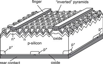
FIGURE 7 The PERL cell, which took efficiency above 24% in the early 1990s.
Since then, further improvements in PERL cells have taken their efficiency to 25% [29], which remains the highest to date for a silicon cell. Major improvements include the growth of much thinner oxide for top-surface passivation which allows the direct application of a double-layer antireflection coating to increase short-circuit current [12], the use of an Al-based “alnealing” sequence for this top oxide and localised top-contact points to increase open-circuit voltage, improved rear-surface passivation and reduced metallisation resistance to improve fill factor.
2.4 PERL Cell Design Features
To maximise performance, as much light as possible of useful wavelengths should be coupled into and absorbed by the cell. Modern cell designs such as the PERL cell (Figure 7) incorporate several primarily optical features to achieve this result.
The inverted pyramids along the top surface serve primarily in such an optical role. Most light incident on this structure will hit one of the sloping side walls of the pyramids at the first point of incidence with the majority of this light coupled into the cell. That reflected will be reflected downward, ensuring that it has at least a second chance of entering into the cell. More than 40% of the light such as incident near the bottom and corners of the pyramids has three such chances. The pyramids are covered by an oxide layer of appropriate thickness to act as a quarter-wavelength antireflection coating. Alternatively, this oxide can be grown thin and a double-layer antireflection coating applied [12].
Light coupled into the cell moves obliquely across the cell toward the rear surface with most absorbed on the way. Weakly absorbed light reaching the rear is reflected by the very efficient reflector formed by the combination of the rear oxide layer covered by an aluminium layer [30]. The reflectance from this combination depends upon the angle of incidence of the light and the thickness of the oxide layer but is typically above 95% for angles of incidence close to the normal, decreasing to below 90% as the incidence angle approaches that for total internal reflection at the silicon/oxide interface (24.7°), and increasing to close to 100% once this angle is exceeded.
Light reflected from the rear then moves toward the top surface. Some reaching this surface strikes a face of a pyramid of opposite orientation to that which coupled it into the cell. Most of this immediately escapes from the cell. Light striking any other pyramid face is totally internally reflected. This results in about half the light striking the top surface internally at this stage being reflected back across the cell toward the rear contact. The amount of light escaping after the first double pass depends on the precise geometry involved. It can be reduced by destroying some of the symmetries involved—for example, by using tilted inverted pyramids or by using a “tiler’s pattern” [30]. The latter approach is currently used in current PERL cell designs.
The combination of the inverted pyramids and the rear reflector therefore forms a very efficient light-trapping scheme, increasing the path length of weakly absorbed light within the cell. Effective path-length enhancement factors [30] above 40 compared to a single pass across the cell are measured. This light trapping boosts the infrared response of the cell. The external responsivity (amps per watt of incident light) of PERL cells peaks at longer wavelengths at higher values than previous silicon cells with values of 0.75 A/W measured at 1.02 μm wavelength. Energy-conversion efficiency under monochromatic light peaks at the same wavelength with values above 45% measured [31]. Further improvements could push this figure to above 50% at 1.06 μm.
Other optical losses are due to reflection from, and absorption in, the top metal fingers of the cell. This can be minimised by making these lines as fine as possible with, ideally, as large an aspect ratio (height to width ratio) as possible. Alternatively, optical approaches can be used to steer incoming light away from these lines or to ensure that light reflected from them eventually finds its way to the cell surface [32,33].
Present PERL cells lose about 5% of incoming light due to absorption or reflection loss associated with these metal fingers when combined with reflection from the unmetallised top surface of the cell. They also lose 1–2% in performance from the use of a less than optimal light-trapping scheme and from less than 100% reflection of light from the rear surface of the cell. There is therefore some scope for small to moderate gains in performance by further improving the optical properties of these cells.
Although such advanced cell designs have been used for spacecraft and high-value terrestrial applications such as solar car racing, the multiple photolithographic steps required in their fabrication make them too expensive for low-cost terrestrial applications [34,35]. They do, however, provide a reference point for the discussion of the compromises involved in lower-cost designs, as discussed in the following sections.
3 Screen-Printed Cells
3.1 Structure
The structure of a standard crystalline screen-printed cell is shown in Figure 3. The normal cell-processing sequence would consist of [36] saw-damage removal from the starting wafer by etching; chemical texturing of the top surface; top-surface diffusion to about 40–60 ohms/square; etching to remove diffusion oxides and the junction at the rear of the cell; deposition of a silicon nitride antireflection coating to the top cell surface; screening and drying of three metal layers sequentially, including a localised Ag rich region on the rear of the cell to allow soldering; an Al rich paste over the rest of the rear and a Ag rich paste on the front side to form the fingers and busbars; simultaneous firing of these layers; and cell testing and sorting.
The typical metallisation pattern used for such cells is shown in Figure 8. Using the normal boron-doped Czochralski silicon wafers of 0.5–5-Ω-cm resistivity, the resulting cell efficiency is typically 16–18%, while for multicrystalline wafers of similar resistivity efficiency is in the 15–17% range.
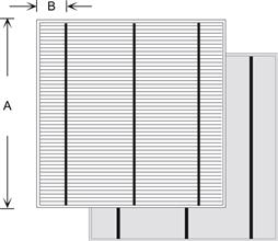
FIGURE 8 Standard 156 mm×156 mm solar cell “H” metallisation pattern. Screen-printed silver regions are shown coloured black. The pattern consists of six unit cells of size A×B.
The major disadvantages of the screen-printing approach relate to the cost of the metal pastes used in the process [37] and the relatively low cell efficiency that results. The low efficiency is due most fundamentally to the restricted line width possible by screen printing. The relatively high contact resistance between the paste and the silicon is another constraint. The low aspect ratio (height/width) of the final lines due to paste thickness shrinkage during firing is another problem compounded by the low conductivity of the fired paste (up to 3 times lower than that of pure silver).
There have been several investigations of the feasibility of screening pastes other than those based on silver. Nickel and copper have been investigated without success to date [38,39]. The contact resistance between the paste and silicon can be a sensitive function of the precise firing environment and temperature, as well as of the doping of the contacted region. The glass frit (dispersed glass particles used in the paste as a binder) forms an oxide precipitate along the interface between the screened paste and the silicon surface. This contributes to the high contact resistance, although often phosphorus is added to the paste to decrease the contact resistance to n-type material.
The rear-surface contact resistance is generally less of a problem. Even though contact is being made to more lightly doped material, a much larger contact area is available. Generally, as previously mentioned and shown in Figure 8, a small region of the rear is printed with a silver-rich paste to allow soldering of the cell interconnect to these regions. The remainder of the rear is printed with an aluminium paste used to increase the doping level in the surface region by alloying. After firing, a significant back-surface-field effect can be obtained by the use of such aluminium.
3.2 Typical Screen-Printed Cell Performance
Typically, the screen-printing approach will produce cell open-circuit voltages in the 600- to 630-mV range, depending on substrate resistivity, short-circuit current densities in the 30- to 36-mA/cm2 range and fill factors for large area cells in the 72–78% range. For a large area cell, typically 10% of the top surface of the cell will be shaded by the screened metallisation and busbars. The top-surface metallisation as indicated in Figure 8 typically consists of metal fingers of about 100–150 microns width, spaced about 2–3 mm apart. Due to the low conductivity of the paste, an interconnect busbar or H-pattern design is mandatory for large area cells. Although contributing to the large shading loss of this approach, this design also has the advantage of improving the cell tolerance to cracks. When scaling to large area cells, the number of busbar interconnections is increased.
To maintain reasonable contact resistance, quite low sheet resistivities for the top-surface diffusion are required. The 50- to 60-Ω/square typically used results in a significant loss in blue response of the cells due to dead layers along the surface. Higher sheet resistivities will improve the blue response but at the expense of cell fill factor. The heavy diffusion also limits the open-circuit voltage output of the cells. Oxide surface passivation is not of much benefit in improving performance due to this limitation. Using improved quality substrates such as float-zone silicon also generally do not result in any substantial performance improvement for screen-printed cells again due to this limitation.
3.3 Improved Screen-Printing Technology
3.3.1 Improved Pastes
The limitations of the screen-printing approach may not be fundamental but may be able to be overcome by ongoing development. Paste manufacturers have quite ambitious plans for improving the performance of their pastes. The aim is to improve the ability of pastes to better contact much lighter top-surface diffusions, with the ability to contact 100-Ω/square emitters targetted by the end of the decade [40].
3.3.2 Selective Emitter and Double Printing
In addition to the improvements in screen-printing pastes over the last decade, there have been substantial improvements in screen-printing equipment. In particular, it is now possible to align printed features very accurately.
This improved alignment accuracy allows the implementation of higher efficiency structures. In particular, the selective-emitter structure of Figure 9(a) now can be implemented in a number of different ways [41]. The end result is a heavily doped emitter region underlying the contact region for the top-surface metallisation fingers. This ensures good contact resistance while allowing other regions of the emitter to be more lightly doped, improving blue response. A gain of 1% absolute (e.g., from 18% to 19% energy conversion efficiency) results from the additional processing involved.

FIGURE 9 The selective-emitter approach.
Another possibility made possible by improved alignment accuracy is “double printing,” which is illustrated in Figure 9(b). By printing the top metallisation fingers twice, the aspect ratio (height/width) of these fingers can be improved, decreasing the resistance loss associated with these fingers. Additionally, the underlying layer can be optimised for low-contact resistance to silicon while the second layer can be optimised for good lateral conduction. Gains are more modest compared to the use of selective emitters, with about 0.2–0.3% absolute gain in efficiency.
3.3.3 Hot-Melt and Stencil Printing
In hot-melt printing, similar pastes to conventional printing are used but these are solid at room temperature. The paste is heated to 60–75 °C during the screen-printing step using heated screen-printing equipment and screens; the paste solidifies as it cools after printing without needing the normal drying step. The key advantage is a higher aspect ratio with an efficiency gain of up to 1% absolute reported [42]. Several pastes manufacturers now sell suitable pastes.
Stencil printing offers both higher aspect ratio and finer line width. Instead of using a metal mesh mask covered with a patterned emulsion as the screen-printing mask, a patterned metal mask is used allowing a wider range of mask properties. An improvement in both current output and paste utilisation has been claimed [43].
3.3.4 Plated Seed Layers
Another approach to achieving high aspect ratio and fine line width involves printing a seed layer followed by plating. Since high aspect ratio of the seed layer is not important in this approach, this layer can be printed with quite narrow line width. Alternatively, more adventurous approaches such as aerosol or ink-jet printing [44] can be used to print this layer. After deposition of the seed layer by any of these techniques, it can be plated to a much larger cross-section either with Ag or with less-expensive metals such as Cu, with a thin Sn or Ag overcoating to temper the reactivity of copper [45]. The use of such approaches may become mandatory to reduce sensitivity to volatile Ag prices [36].
3.4 Screen-Printing Limitations
Despite the potential for improvement outlined above, it is doubtful that an extremely high-efficiency cell can ever be produced using the screen-printed approach, with the best cells combining all available options expected to give only 19–20% efficiency. Even if both the line width and the contact-resistance problems are successfully solved in production, there are still challenges due to conductivity and small aspect ratio.
Perhaps even more important, there is a looming issue with Ag supply. The 2010 production of more than 20 GW of silicon photovoltaics corresponded to the use of close to 2000 tonnes of Ag in this product, from a total of 28,600 tonnes of Ag supply [36]. If module production continues to double every year or two, considerable pressure will be placed on Ag supply in the coming decade with a continuation or even an acceleration of the rapid escalation in Ag price seen over recent years. A major change in the way most cells have been made for more than 30 years seems essential over the coming decade.
4 Laser-Processed Cells
4.1 Buried-Contact Cells
The buried-contact solar cell of Figure 10 was developed to overcome the efficiency limitations of the screen-printed cell approach. The most distinctive feature of this approach is the use of laser-defined grooves in the top surface to locate the cell metallisation. Although originally investigated using screen-printed metallisation sequences (where the metal was forced into the groove during the screening operation), the most successful designs have used electrolessly plated metal contacts [46].

FIGURE 10 Buried-contact solar cell.
Cell processing bears some resemblance to the screen-printing sequence previously described. After saw-damage removal and texturing, the surface is lightly diffused and an oxide is grown over the entire surface and a nitride antireflection coating is deposited. This dielectric layer serves multiple purposes during cell processing and is the key to the relative simplicity of the processing. Grooves are then cut into the top cell surface using a laser scribing machine, although mechanical cutting wheels [47] or other mechanical or chemical approaches could be used.
After cleaning of the grooves by chemical etching, these are subject to a second phosphorus diffusion, much heavier than the first. This produces selective doping in the contact areas. Aluminium is then deposited on the rear surface by evaporation, sputtering, screen printing, or plasma deposition.
After firing of the aluminium and etching to remove oxides, cell metallisation is then completed by electroless plating of a nickel–copper–silver layer. A thin layer of nickel is first deposited. This is then fired, and a substantial thickness of copper is then deposited. Finally, the thin layer of silver is formed on the top surface by displacement plating. All these processes can be electroless, meaning that canisters containing the wafers are simply immersed in the plating solution.
The first commercial use of buried-contact cell technology was when a high-efficiency array was fabricated by Telefunken [48] for the Swiss car “Spirit of Biel,” which convincingly won the 1990 World Solar Challenge, the solar car race from Darwin to Adelaide. Array efficiency was 17%, then the highest ever for silicon. The array gave 25% more power than that of the second-place car, which used enhanced screen-printing technology [49].
BP Solar has reported on both manufacturing yields and process economics [50]. Using the same “solar grade” CZ substrates as in its screen-printing process, BP reported substantial efficiency improvement for the technology (circa 30%) and cell efficiencies of 17.5–18%. Economic analysis shows that the approach, as developed by BP with nitride antireflection coating, is well suited for polycrystalline material [50]. In 1994, BP Solar launched the Saturn 585 module, an 85-W module based on 123-mm-square buried-contact solar cells as its “top-of-the-line” commercial product [51], with module size subsequently doubled to 170 W. Production capacity at BP Solar peaked in 2003 when 50 MW/year of buried-contact cells were manufactured, about 3% of total world production.
The consensus of production experience is that the buried-contact process can give a substantial efficiency margin over screen printing. Although more processing steps are involved than in the simplest screen-printing approach, expensive silver pastes are eliminated so that processing costs per unit area are not greatly different, with costs per watt of product lower [34,35]. Marketing experience has shown that higher-selling prices are feasible for this product due to the lower balance of systems costs in installed systems and the perceived higher quality due to the superior performance.
4.2 Semiconductor Finger Solar Cell
The semiconductor finger solar cell shown in Figure 11 incorporates the advantages of either the buried-contact solar cell of the previous section or the laser-doped solar cell of the following section while retaining a standard screen-printed contacting approach.
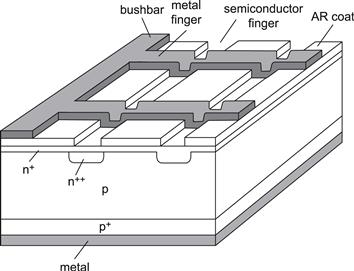
FIGURE 11 Semiconductor finger solar cell. Heavily doped semiconductor regions provide an additional layer of fingers contacted by the traditional metal finger layer.
In the buried-contact variant, the initial steps prior to metallisation are similar to those in the previous section. Metallisation however is applied by screen printing with the printed Ag top contact running perpendicular to the grooves as shown in Figure 11. Paste composition in this case would be selected so that the paste did not fire through the dielectric, reducing contact area. It would, however, contact the exposed, heavily doped regions in the grooves. Cell efficiency in the 18–19% range has been reported in large-scale pilot production using the approach.
A simpler version uses the laser-doped, selective-emitter sequence of the following section to form the “semiconductor” fingers with similarly good outcomes.
4.3 Laser-Doped, Selective-Emitter Solar Cells
The laser-doped, selective-emitter (LDSE) cell [52] uses a laser scan to both dope the emitter selectively in regions scanned as well as to remove the overlying dielectric to expose the silicon surface, allowing selective contacting to this exposed surface region as shown in Figure 12.

FIGURE 12 Laser-doped selective-emitter (LDSE) solar cell [18]. Metal is selectively plated to the heavily doped regions exposed during the laser-doping step.
The processing starts as for a selective-emitter, screen-printed or buried-contact cell, with the initial top-surface diffusion quite light, to maintain good blue response in the completed cell. After deposition of the top-surface dielectric, the top surface is scanned by a laser to produce the selective emitter and to remove the dielectric in the scanned area. The dopant source could be from within this dielectric, from a doped layer deposited on top of the dielectric, or even in liquid form mixed in the water jet sometimes used to guide the laser in such applications.
Electroless or electrolytic plating can be used to produce Ni–Cu–Ag or related layers confined to the regions scanned by the laser, as described in connection with the buried-contact cell of Section 4.1.
The combination of selective-emitter, narrow, conductive top-finger metallisation and the good surface passivation possible with this approach results in excellent final performance with efficiencies more than 19% confirmed for cells manufactured on a commercial production line apart from the laser-processing steps. Efficiencies above 20% are anticipated using “double-sided” versions of the technology.
5 HIT Cell
The HIT cell combines both crystalline and amorphous silicon cell technology to produce high-conversion-efficiency cells in production and also some of the highest-efficiency large-area laboratory devices ever reported. The basic device structure is shown in Figure 13.
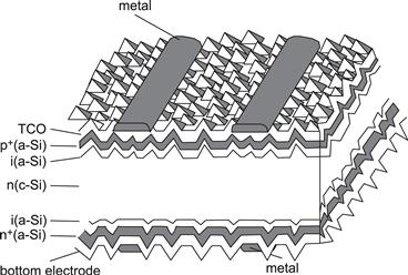
FIGURE 13 HIT cell structure using a textured n-type silicon wafer with amorphous silicon heterojunctions on both front and rear surfaces.
The starting substrate is an n-type silicon wafer, the opposite polarity from most previous commercial product. This is a fortunate choice since such substrates are free from the light-induced degradation effects that limit the performance of cells made on p-type, boron-doped substrates attributed to the formation of boron–oxygen complexes under illumination [53]. The n-type substrates are also more tolerant to Fe, a common substrate impurity. After texturing, very thin layers of intrinsic hydrogenated and p-type amorphous silicon (a-Si) are deposited on the top surface and intrinsic and n-type a-Si on the rear surface. As is usual in amorphous silicon technology, these layers are contacted by transparent conducting oxide (TCO) layers, in turn contacted by screen-printed metal contacts.
The low sheet resistivities possible with these TCO layers relax the constraints previously described on the screen-printed metallisation parameters. However, the TCO layers are more absorbing than Si3N4, and the underlying doped layers of amorphous silicon are inactive for photocurrent collection, resulting in poor blue response of the cell. About 10% of available current is lost by absorption in these layers. However, the band gap of amorphous silicon is very much higher than in silicon, and the quality of the interface between the amorphous and crystalline material is excellent. This has produced some of the highest open-circuit voltages seen in silicon cells (up to 745 mV).
This approach has produced record large-area laboratory cell performances of up to 23.0% [54]. The differences between these laboratory devices and the less highly performing commercial product are not clear. Commercial modules are offered in the 16.1–19.0% total area efficiency range [1]. Sanyo produced an estimated 300 MW of HIT cell product during 2010 [55].
6 Rear-Contacted Cells
The first solar cell of the modern photovoltaic era had both contacts on the rear [30]. The design subsequently evolved to bifacial contacts (Figure 2) to reduce resistance losses. There has, however, long been an interest in reverting to designs with both contacts on the rear since this offers scope for more densely packing cells and for simplifying cell interconnection.
The initial rear-contact cell can be described as an “emitter wraparound” cell, part of a more general class of emitter wrap-through (EWT) cells that have no metal on the top surface. An alternative approach is the metal wrap-through (MWT) cell where both front and rear surfaces of the cell are metallised but the top metallisation connects through holes in the cell to the appropriate polarity rear contact. However, the most successful rear contact cell to date has been a more sophisticated design initially suggested by Schwartz [56] with both polarity junctions on the rear surface.
6.1 Rear-Junction Solar Cells
As previously mentioned, the first silicon cell to demonstrate efficiency above 22% was the rear-point contact cell of Figure 6 developed at Stanford University. With some simplifications to the rear-contacting scheme [57], this approach has now been commercialised as the mainstream product offered by a major silicon cell and module manufacture, SunPower, with its cell structure shown in Figure 14.
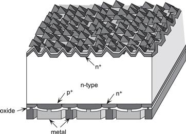
FIGURE 14 SunPower rear-junction solar cell.
Using this cell, SunPower offers modules of 18.4–19.7% total area efficiency [1], where the area includes the module frames. These are presently the highest-efficiency commercial modules available by a clear margin. Recently, a large-area cell (225 cm2) with some improved features was measured at 24.2% efficiency, the highest ever for a cell of this size [58].
The rear-junction approach to rear contact cell design is quite challenging. The silicon wafer has to be both thin and of good quality, and both front and rear surfaces must have good surface properties. Most carriers in a silicon cell are generated within the first 2 microns of entering the cell. The wafer and surface quality needs to be good so these carriers can find their way to the rear contact without recombining. Minority-carrier diffusion lengths have to be at least 5 times the wafer thickness to keep the loss of these migrating carriers to less than 2%. As such, the approach is not suited to multicrystalline or lower-solar-grade materials but results in excellent cells on good-quality materials.
6.2 Emitter Wrap-Through (EWT) Cells
As previously noted, the silicon cells that introduced the modern photovoltaic era are related to modern EWT designs.
For EWT cells, there is no metal on the top surface of the cell with the top-surface dopant providing the contact path to the rear as shown in Figure 15(a). The advantages are zero shading by metal on the top surface plus closer cell packing and simplified cell interconnection. The disadvantage is the high density of holes required due to the relatively poor conductivity of the top layer. The MWT cell of the following section is closely related but does not require as many through-wafer contacts.
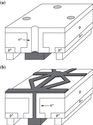
FIGURE 15 (a) Emitter wrap-through (EWT) and (b) metal wrap-through (MWT) cells.
6.3 Metal Wrap-Through (MWT) Cells
The metal wrap-around cell has been investigated from the 1960s for space use, given the clear advantages of having both cell contacts on the rear. Of more interest for terrestrial use has been the metal wrap-through (MWT) cell with metal on both surfaces connected by holes through the wafer (Figure 15(b)).
Advantages are reduced shading of the front surface of the cell since thick busbars are eliminated, closer cell packing, and simplified module assembly. Disadvantages are the extra processing required in drilling holes through the cell by laser.
Unlike the rear-junction cells of Section 6.1, MWT cells are well suited to low-quality substrates. In fact, the first solar modules of more than 17% aperture area efficiency using multicrystalline wafers were fabricated using MWT cells [59].
7 Conclusions
With the costs of present wafer-based silicon approaches dominated by material costs, particularly those of the wafers, encapsulants, low-iron tempered glass superstrates, and metal pastes, increasing cell efficiency is an effective, if often counterintuitive, approach to reducing the cost of the final product.
Recent years have seen a diversification of manufacturing into higher-efficiency approaches. Quite revolutionary departures from the standard approach have been made by BP Solar, with its former top-of-the-line Saturn processes, based on laser-grooved buried contacts; by Sanyo, with its crystalline–amorphous silicon hybrid HIT cells; SunPower, with the company’s very-high-performance rear-junction cells; and, more recently, Suntech with its Pluto cell [60].
In mainstream production, there is still a large potential to capture more of the improvements in silicon cell performance that have been demonstrated in the laboratory. The escalating price of Ag over recent years is likely to require a response from across the photovoltaic manufacturing industry, which may finally induce the industry to depart from the screen-printing process that has been its backbone for more than 30 years.
To reduce Ag consumption, a transition to Cu seems mandatory over the coming decade, whether by plating Cu to layers applied themselves by plating approaches or by screen printing or related physical deposition processes.
The laser-processing approaches, such as demonstrated by the buried-contact solar cell and, more recently, the laser-doped, selective-emitter cell, seem the natural choice for such plating sequences, particularly given their demonstrated high-efficiency potential.
The limiting efficiency of cells relying on traditional Al rear contacts lies in the 21–22% range, as demonstrated by the best laboratory devices using this approach. To progress closer to the 25% efficiency value that may ultimately be achievable in production by a silicon device, a more sophisticated rear-contacting approach is required. Double-sided laser-processed approaches are again a promising option in this area.
Acknowledgements
The author gratefully acknowledges support by an Australian Government Federation Fellowship in the initial stages of this work and thanks the School of Photovoltaic and Renewable Energy Engineering for permission to reproduce material and figures from the author’s text Silicon Solar Cells: Advanced Principles and Practice.
References
1. Haase C, Podewils C. More of everything: market survey on solar modules 2011. Photon Int February 2011;:174–221.
2. Smith KD, Gummel HK, Bode JD, Cuttriss DB, Nielson RJ, Rosenzweig W. The solar cells and their mounting. Bell Sys Tech J. 1963;41:1765–1816.
3. Iles PA. Increased output from silicon solar cells. Seattle: Conference Record, Eigth IEEE Photovoltaic Specialists Conference; 1970; pp. 345–352.
4. Gereth R, Fischer H, Link E, Mattes S, Pschunder W. Silicon solar technology of the seventies. Seattle: Conference Record, Eigth IEEE Photovoltaic Specialists Conference; 1970; p. 353.
5. Gereth R, Fischer H, Link E, Mattes S, Pschunder W. Contribution to the solar cell technology. Energy Conversion. 1972;12:103–107.
6. Mandelkorn J, Lamneck JH. A new electric field effect in silicon solar cells. J Appl Phys. 1973;44:4785.
7. Godlewski MP, Baraona CR, Brandhorst HW. Low-high junction theory applied to solar cells. Palo Alto: Tenth IEEE Photovoltaic Specialists Conference; 1973; pp. 40–49.
8. Lindmayer J, Allison J. The violet cell: an improved silicon solar cell. COMSAT Tech Rev. 1973;3:1–22.
9. Haynos J, Allison J, Arndt R, Meulenberg A. The comsat non-reflective silicon solar cell: a second generation improved cell. Hamburg: International Conference on Photovoltaic Power Generation; September, 1974; p. 487.
10. H.G. Rudenberg, B. Dale, Radiant energy transducer, US Patent 3,150,999 (filed 17 February, 1961).
11. Ralph EL. Recent advancements in low cost solar cell processing. Conference Proceedings Scottsdale: Eleventh IEEE Photovoltaic Specialists Conference; 1975; 315–316.
12. Zhao J, Green MA. Optimized antireflection coatings for high efficiency silicon solar cells. IEEE Trans Electron Devices. 1991;38:1925–1934.
13. Fossum JG, Burgess EL. High efficiency p+ n n+ Back-surface-field silicon solar cells. Appl Phys Lett. 1978;33:238–240.
14. Godfrey RB, Green MA. 655mV open circuit voltage, 17.6% efficient silicon MIS solar cells. Appl Phys Lett. 1979;34:790–793.
15. Green MA. Enhancement of schottky solar cell efficiency above its semiempirical limit. Appl Phys Lett. 1975;28:268–287.
16. Lindmayer J, Allison JF. Dotted contact fine geometry solar cell. U.S Patent 3,982,964 September 1976.
17. Arndt RA, Meulenberg A, Allison JF. Advances in high output voltage silicon solar cells. Orlando: Conference Record, Fifteenth IEEE Photovoltaic Specialists Conference; 1981; pp. 92–96.
18. Green MA, Blakers AW, Shi J, Keller EM, Wenham SR. High-efficiency silicon solar cells. IEEE Trans on Electron Devices ED-31 1984;671–678.
19. Lindholm FA, Neugroschel A, Arienze M, Iles PA. Heavily doped polysilicon– contact solar cells. Electron Device Lett EDL-6 1985;363–365.
20. Yablonovitch E, Gmitter T, Swanson RM, Kwark YH. A 7209mV open circuit voltage, SiOX:c–Si:SiOX double heterostructure solar cell. Appl Phys Lett. 1985;47:1211–1213.
21. Van Halen P, Pulfrey DL. High-gain bipolar transistors with polysilicon tunnel junction emitter contacts. IEEE Trans. on Electron Devices. 1985;32:1307.
22. Tanaka M, Taguchi M, Takahama T, et al. Development of a new heterojunction structure (ACJ-HIT) and its application to polycrystalline silicon solar cells. Prog Photovolt. 1993;1:85–92.
23. Blakers AW, Green MA. 20% Efficiency silicon solar cells. Appl Phys Lett. 1986;48:215–217.
24. Saitoh T, Uematsu T, Kida T, Matsukuma K, Morita K. Design and fabrication of 20% efficiency, medium-resistivity silicon solar cells. New Orleans: Conference Record, Ninteenth IEEE Photovoltaic Specialists Conference; 1987; pp. 1518– 1519.
25. Callaghan WT. Evening presentation on Jet Propulsion Lab Photovoltaic activities. Sevilla: Seventh E.C. Photovoltaic Solar Energy Conference; Oct., 1986.
26. Sinton RA, Kwark Y, Gan JY, Swanson RM. 27.5% Si concentrator solar cells. Electron Device Lett EDL-7 1986;567.
27. King RR, Sinton RA, Swanson RM. Front and back surface fields for point- contact solar cells. Las Vegas: Conference Record, twentieth IEEE Photovoltaic Specialists Conference; September, 1988; pp. 538–544.
28. Blakers AW, Wang A, Milne AM, Zhao J, Dai X, Green MA. 22.6% Efficient silicon solar cells. Sydney: Proceedings, Fourth International Photovoltaic Science and Engineering Conference; February, 1989; pp. 801–806.
29. Green MA. The path to 25% silicon solar cell efficiency: history of silicon cell evolution. Prog Photovolt: Res Appl. 2009;17(3):183–189.
30. Green MA. Silicon Solar Cells: Advanced Principles and Practice. Sydney: Bridge Printery; 1995.
31. Green MA, Zhao J, Wang A, Wenham SR. 45% Efficient silicon photovoltaic cell under monochromatic light. IEEE Electron Device Lett. 1992;13:317–318.
32. Green MA, Zhao J, Blakers AW, Taouk M, Narayanan S. 25-percent efficient low-resistivity silicon concentrator solar cells. IEEE Electron Device Lett EDL-7 1986;583–585.
33. Cuevas A, Sinton RA, Swanson RM. Point- and planar-junction p-i-n silicon solar cells for concentration applications, fabrication, performance and stability. Kissimmee: Conference Record, Twenty-first IEEE Photovoltaic Specialists Conference; May, 1990; pp. 327–332.
34. Bruton T, Luthardt G, Rasch K-D, et al. A study of the manufacture at 500mwp p.a of crystalline silicon photovoltaic modules. Barcelona: Conference Record, Fourteenth European Photovoltaic Solar Energy Conference; June–July, 1997; pp. 11–26.
35. Bruton TM. MUSIC FM five years on: fantasy or reality?. Rome: PV in Europe; October 2002.
36. Neuhaus D-H, Münzer A. Industrial siliconwafer solar cells. Adv OptoElectronics 2007;1–15 Article ID 24521.
37. M.A.Green, Ag requirements for silicon wafer-based solar cells, Prog. Photovolt., accepted for publication.
38. Firor K, Hogan S. Effects of processing parameters on thick film inks used for solar cell front metallization. Solar Cells. 1981–1982;5:87–100.
39. Final Report. Flat Plate Solar Array Project. Jet Propulsion Laboratory, Publication 86–31. October, 1986;Vol. V.
40. Crystalline Silicon PV Technology and Manufacturing Group. International Technology Roadmap for Photovoltaics: Results 2010. Second ed. Berlin: SEMI PV Group Europe; March 2011.
41. Chunduri SK. New choices for ‘Selective’ shoppers. Photon Int December 2010;158–172.
42. H. Kerp, K. McVicker, B. Cruz, P. Van Eijk, D. Arola, E. Graddy, et al., Leading high aspect ratio front contact metallization techniques for crystalline silicon solar cells, Proceedings of the Twenty-fifth European Photovoltaic Solar Energy Conference and Exhibition, 6–10 September 2010, Valencia, Spain, pp. 2460–2463.
43. B. Heurtault, J. Hoornstra, Towards industrial application of stencil printing for crystalline silicon solar cells, Proceedings of the Twenty-fifth European Photovoltaic Solar Energy Conference and Exhibition, 6–10 September 2010, Valencia, Spain, pp. 1912–1916.
44. J. Ebong, B. Renshaw, I. B. Rounsaville, K. Cooper A. Tate, S. Rohatgi, et-al., Ink jetted seed and plated grid solar cells with homogeneous high sheet resistance emitters, Proceedings of the Twenty-fifth European Photovoltaic Solar Energy Conference and Exhibition, 6–10 September 2010, Valencia, Spain, pp. 2390–2394.
45. J. Bartsch, A. Mondon, C. Schetter, M. Hörteis, S. W. Glunz, Copper as conducting layer in the front side metallization of crystalline silicon solar cells—challenges, processes and characterization, Proceedings of the Second Workshop on Metallization, April 14th & 15th, 2010, Constance, Germany, pp. 32–37.
46. Wenham SR. Buried-contact silicon solar cells. Prog Photovolt. 1993;1:3–10.
47. Wohlgemuth J, Narayanan S. Buried contact concentrator solar cells. Las Vegas: conference record, twenty-second IEEE Photovoltaic Specialists Conference; 1991; pp. 273–277.
48. Boller H-W, Ebner W. Transfer of the BCSC-Concepts into an industrial production line. Freiburg: Proceedings of the Ninth E.C. Photovoltaic Solar Energy Conference; 1989; September, pp. 411–413.
49. Kyle C. Racing with the sun: The 1990 world solar challenge. Engineering Society for Advancing Mobility: Land, Sea, Air and Space, SAE Order No. R-111 1991.
50. Bruton TM, Mitchell A, Teale L. Maximizing minority carrier lifetime in high efficiency screen printed silicon bsf cells. Lisbon: Conference Proceedings, Tenth E.C. Photovoltaic Solar Energy Conference; April, 1991; pp. 667–669.
51. BP Saturn product sheet, April, 1994.
52. Wenham SR, Green MA. Self aligning method for forming a selective emitter and metallization in a solar cell. United States Patent US6,429,037 B1 6 August 2002.
53. Schmidt J, Bothe K. Structure and transformation of the metastable boron- and oxygen-related defect center in crystalline silicon. Phys Rev B. 2004;69 0241071–02410718.
54. Maruyama E, Terakawa A, Taguchi M, et al. Sanyo’s challenges to the development of high-efficiency HIT solar cells and the expansion of HIT business. Hawaii: Proceedings of the Fourth World Conference on Photovoltaic Energy Conversion (WCEP-4); May 2006.
55. Hering G. Year of the tiger: PV cell output roared in 2010 to over 27gw—beating 2006 through 2009 combined—but can the year of the rabbit bring more multiples?. Photon Int March 2011;186–218.
56. Schwartz RJ. Review of silicon solar cells for high concentrations. Solar Cells. 1982;6:17–38.
57. Mulligan WP, Cudzinovic MJ, Pass T, et al. Solar cell and method of manufacture. United States Patent US7,897,867 B1 1 March 2011.
58. Cousins PJ, Smith DD, Luan HC, et al. Gen III: Improved Performance at Lower Cost. Honolulu: Proceedings of the Thirty-fifth IEEE PVSC; June 2010.
59. Lamers MWPE, Tjengdrawira C, Koppes M, et al. 17.9% Metal-wrap-through mc-si cells resulting in module efficiency of 17.0%. Prog Photovolt., article first published online. March 2011;23 j http://dx.doi.org/10.1002/pip.1110; March 2011.
60. Shi Z, Wenham SR, Ji JJ. mass production of the innovative PLUTO solar cell technology. Philadelphia: Proceedings of the Thirty-fourth IEEE Photovoltaic Specialists Conference; June 2009; 7–12.