
Chapter IB-1
Crystalline Silicon
Manufacture and Properties
Chapter Outline
2. Characteristics of Silicon Wafers for Use in PV Manufacturing
2.1. Geometrical Specifications
4. Crystal-Preparation Methods
1 Introduction
The majority of silicon wafers used for solar cells are Czochralski (CZ) single crystalline and directional solidification, or cast, multicrystalline (mc) material. The split between the two types of wafer is presently about 55% mc-Si and 45% CZ-Si. Until 1995, CZ wafers represented 60% of the substrates used by industry and mc-Si wafers around 25%. The fast scale-up of commercially available multicrystalline wafers changed the picture rapidly. The remainder of the silicon substrates used by the industry are nonwafered sheets or ribbons that are of different types and have recently gained significant production figures following long development phases. Nonwafer silicon accounted for about 4% of the market in 2001, up from 1–2% in the mid-1990s [1,2].
2 Characteristics of Silicon Wafers for Use in PV Manufacturing
2.1 Geometrical Specifications
Most of the wafer substrates used in production facilities have dimensions relating to the diameters of monocrystalline silicon cylinders for the semiconductor industry (essentially 5 and 6 inches) that, in turn, have influenced standards for wafer carriers, automation, packaging, etc. However, in order to maximise the power density of the modules, wafers are square, or pseudo-square in the case of monocrystalline silicon—that is, cylinders are shaped as squares with rounded-off corners. This reduces the surface area of the wafers by between 2% and 5% compared with a full square of same dimensions.
In the case of mc-Si, ingot sizes are designed to be compatible with multiple numbers of each of the standard wafer dimensions in order to maximise geometrical yield. Yield considerations limit the possible wafer sizes achievable for any given ingot dimension, as much as expensive wafer cassettes, automation, and packaging do later in the process. Table 1 reports the different sizes for commercially available wafers, including typical tolerances.
TABLE 1 Commercially Available Wafer Sizes
A SEMI™ (Semiconductor Equipment and Materials International) standard, M61000, was developed with the purpose of covering the requirements for silicon wafers for use in solar cell manufacturing [3], including dimensional specifications, defects, and electronic properties. Most commercial suppliers sell their wafer products using specifications that are close to those described by M61000. However, smaller wafers are usually 103 mm rather than 100 mm as specified, and there are some notable exceptions to the specifications—e.g., dimensions of wafers produced in-house by some of the early players who have developed their own standard and do not usually buy wafers on the market. Another obvious exception is provided by nonwafer substrates, the dimensions of which are in general determined by the growth equipment and the technique. Some manufacturers use rectangular wafers. Other requirements, besides the geometrical definitions of the wafers, are thickness uniformity and reduced levels of cracks and saw marks that could adversely affect later processing.
Typical specifications for commercially available wafers are described in Table 2.
TABLE 2 Other Dimensional Specifications for Typical PV Wafers
| Parameter | Value |
| Thickness of a batch | 530 ± 40 μm |
| Total Thickness Variation (TTV) of a wafer | 50 μm |
| Cracks | <1 mm |
| Saw marks | <10 μm |
| Bow | <50 μm |
The absolute value of the wafer thickness has dropped by about 100 μm in the last decade, as a consistent cost-reduction measure [4,5], and is expected to decrease further in the next years [2] as automation and cell processing become more sophisticated and can allow effective handling of thin wafers. Some wafer and cell producers already have less than 300 μm wafers in their production lines, although in general wafer sizes in such cases are limited to the 100 cm2 range in order to maintain mechanical yields in the high 90s. Similarly to the case of the area dimensions, thickness in nonwafer substrates is determined by the process and is in general less homogeneous, providing one of the major differences between wafer and nonwafer cell technologies. A great deal of effort was put in the last decade in developing automated thickness measurement tools for manufacturing plants to inspect wafer thickness variations in lots, an extremely difficult task in manually inspected wafer-fabrication sequences.
2.2 Physical Specifications
Wafers are generally classified in terms of resistivity, type, and oxygen and carbon content. These data are generally present in all commercial specifications related to single and multicrystalline wafers, and they refer to ASTM or equivalent standards. However, the PV community has had to face the unavoidable departure from standard test conditions of all parameters when measuring the properties of the inherently inhomogeneous nature of multicrystalline wafers, which led to agreement on relatively broad ranges for resistivity or upper thresholds for oxygen and carbon contents. Early concerns, for instance, of the influence of grain boundaries on the determination of resistivity using the four-point probe method are now somewhat more relaxed after significant statistical feedback has provided comfort in the values proposed. Still, in strict terms, standards related to the measurement of resistivity in multicrystalline wafers do not exist, which is true of course for nonwafer silicon technologies as well. This is also true for other kinds of measurements, and the effort to develop meaningful characterisation tools for lower or inhomogeneous quality materials as compared to the semiconductor industry is a clear indication of such a need (see Chapter III-1). Furthermore, the increasing volumes of wafers in the growing PV market has forced a second, big departure from semiconductor wafer characterisation standards, imposing fast, nondestructive test methods to optimise costs and yields. In most cases, for instance, resistivity and type are measured at block rather than at wafer level. Table 3 shows the typical values for physical parameters of commercially available wafers for industrial processing. These are either multicrystalline or monocrystalline Czochralski. Float-zone (FZ) wafers for PV may become commercial products and will be discussed in a later paragraph.
TABLE 3 Physical Specifications of Commercial Silicon Wafers
| Parameter | Value |
| Type | P–boron doped |
| Resistivity | 0.5–3 ohm cm |
| Oxygen (mc-Si) | <8×10¹⁷ at/cm3 |
| Oxygen (CZ-Si) | <1×10¹⁸ at/cm3 |
| Carbon (mc-Si) | <1×10¹⁸ at/cm3 |
| Carbon (CZ-Si) | <2×10¹⁷ at/cm3 |
2.3 Physical Specifications
Minority-carrier lifetime characterisation of commercial silicon is worth a paragraph on its own. This is by far the most complicated parameter to measure and to effectively relate to subsequent processing quality and yield. It is also most influenced by the inhomogeneity of multicrystalline silicon, as well as by thermal treatments. It became immediately evident to all PV manufacturers at the very beginning of the expansion of the multicrystalline silicon market that the identification of an appropriate tool for analysing and understanding the properties of mc-Si would have been one of the keys for the commercial success of the material. A generous number of attempts were made to adapt the existing lifetime measurements—rigorously valid for high-quality polished single crystalline wafers—to provide meaningful values for mc-Si and even CZ-Si for the PV community. Also, as mentioned before, any acceptable test would need to be fast, cost-effective, and obviously nondestructive as the number of samples to inspect was bound to be large. This focussed effort led to the development of a number of automated lifetime analysers, which at the end of the development process had relatively low resemblance with the semiconductor industry counterparts. Probably the most successful commercial methods are the microwave photoconductance decay method (μ-PCD), performed directly on silicon blocks, and the photoconductance decay or quasi-steady state method developed by Ron Sinton, which is discussed in Chapter III-1.
For the purposes of the present chapter, we focus on the μ-PCD characterisation of mc-Si blocks. This measurement technique is commercially available and widely used, although strong debates on the validity of the results occurred for many years. The measurement is based on the detection of the amplitude of the microwave field reflected by the sample surface. This amplitude variation depends on the conductivity, and thus also on the number of minority carriers generated by a short laser pulse [6]. The time in which the system recovers the initial state is associated with the quality of the semiconductor material and with the recombination mechanisms in the bulk and at the surface. It is generally rather complicated to separate different contributions, and PV silicon has peculiar characteristics that enhance difficulties, such as relatively high doping, rough surfaces, and short diffusion lengths for minority carriers. Furthermore, as mentioned before, the industry requirements are for fast nondestructive techniques that enable prediction of later behaviour of the material in the processing line in order to minimise the costs of processing low-quality material as early as possible. For this reason, the industry has pushed towards the use of fast, noninvasive block scanners since the early 1990s, despite the inability of the measurement systems to conform to any of the existing standards. A certain effort has been directed until relatively recently toward developing uniform measurement systems and procedures, which has proved once more the difficulty of the problem [7] and finally led to generally accepted principles subject to bilateral confirmation in the case of commercial relationships between wafer vendors and cell producers.
The main problems with block scanners, besides separation of bulk and surface components, lie in the fact that the measurement is actually performed on a very thin portion of the block. This is due to the absorption of the laser pulse in silicon (usually in the near infrared range) and to the high reflectivity of microwaves, which only allow the field to penetrate a skin depth of the sample under examination. Other difficulties lie in the unpredictable behaviour of the material in three dimensions, lateral distribution of carriers, trapping effects, unknown injection levels, and the macroscopic saw damage affecting the control of the distance of the measurement head from the sample. Microwave block scanners are unable to handle these problems, which are better taken into account by the technique described in Chapter III-1. The experience of crystal growers and the feedback from cell processing lines, however, led to the establishment of a method for the analysis of silicon blocks that is able to reject low-quality material at block level and that allows the identification of the correct cropping position for the rejection of tops and tails.
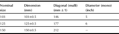
A typical map, performed with a commercially available automated system [8], of a standard block of mc-Si grown by the directional solidification method is shown in Figure 1. The silicon is boron doped to a resistivity corresponding to 1×10¹⁶ at/cm3, and the measurement is performed with a microwave field in the GHz range coupled by an antenna for a sample irradiated by a laser diode pulse at 904 nm.
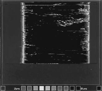
FIGURE 1 Lifetime map.
The absolute value of the minority-carrier lifetime is surface limited, as the sample is measured ‘as cut.’ Normally, in fact, no impractical etching or passivation treatments are applied to the surface, which therefore has a high recombination velocity. It is assumed that the surface is always in the same conditions, so any change in the relaxation time is associated with bulk properties. A map such as the one in Figure 1 takes a few minutes to be realised with a modern lifetime scanner such as the one in [8]. Early systems could take several hours to perform measurements with the same resolution. The low-lifetime regions (in red) have different physical origins, and this is where the extensive material-to-cell correlation work performed over the years has been essential in comfortably introducing these instruments in the production environment [4,5,9]. The red zones at the top, in fact, are determined by the segregation of metals due to the refining process during solidification, and the wafers cannot effectively be used in cell processing, so they are rejected and possibly remelted. The red zones at the bottom of the block are composed of a highly defected area—the initial crystal growth, highly dislocated and unusable for solar cells within about 1 cm from the start—and the 2–3 cm region of oxygen rich material that, despite its low initial lifetime, recovers after the thermal treatments used in cell processing and normally produces good-quality cells. Care must be taken, therefore, to exactly determine the cut off (by any means possible!) between good- and low-quality material at the bottom of the control procedure at block level.
Figure 2 shows a typical correlation between the lifetime at block level and cell performance, being evidence of a good performance of initially low-quality material as detected by the block scanner [9]. The central part of the block is instead relatively uniform and produces good-quality cells, in the range of 12–15%, depending on the particular process used, the higher value provided by silicon nitride–based sequences.
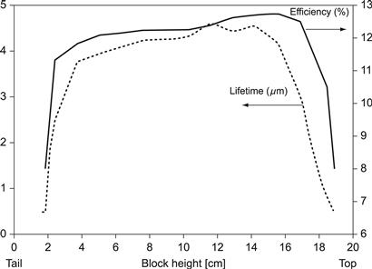
FIGURE 2 Correlation of lifetime with cell efficiency.
Typical values in the central part of the blocks are around 5–10 μs, depending on the specific measurement system used. A fundamental assumption of this method is a relative uniformity of the material in any given region of the block (i.e., all central regions behave similarly in same conditions), which is also a result of extensive correlation work [5,9].
μ-PCD testers are also used to inspect incoming wafers in production lines, and in this case as well there has been important correlation work to be able to confidently accept material for subsequent processing. This applies to CZ-Si wafers, which are inspected for uniformity as well as for the acceptance threshold value (which varies from case to case).
3 Feedstock Silicon
The commercial success of PV is driven critically by its cost. Silicon wafers account for about 50% of the total production cost of a module, a figure that has increased over the years, from the 33% of about 10 years ago, thanks to the constant improvements in technology that have identified the wafer as the ultimate cost-limiting factor [10].
There is no source of silicon feedstock unique to the PV industry, so the issue of a possible feedstock shortage has been largely debated and is still not concluded. About 10–15% of the silicon used by the microelectronics industry is available in various forms for PV use. This is in the range of 1800–2500 tons per year of higher quality scrap and an extra 1500–2000 tons of lower-quality material (e.g., pot scrap). Based on an effective usage rate of 10–15 tons per MWp produced, the amounts considered cannot feed the fast-growing PV market for long. Whilst extensive research programmes have been conducted for many years to upgrade cheap metallurgical silicon to be an independent low-cost silicon source for PV, none of the techniques proposed has reached commercial maturity [5]. The scare of a silicon shortage as early as the middle of the present decade has instead favoured several proposals for processes similar to those used for the production of polysilicon but with looser specifications [11,12].
From a practical point of view, there is, in general, no constraint related to the geometrical specification of the starting material, so for the moment PV can enjoy low-cost scrap such as silicon chips from the cutting processes of semiconductor manufacturing, popcorn silicon rods, tops and tails from crystal growth processes, etc. [13].
However, different crystallisation methods require different specifications. In general, monocrystalline and nonwafer technologies require high-quality starting material, while the multicrystalline technology can allow a looser specification if some care is taken, due to its purifying characteristics—another point in its favour.
4 Crystal-Preparation Methods
A number of techniques are available for the production of silicon wafers for the PV industry: CZ-Si and multicrystalline silicon (which have already been mentioned), magnetically confined multicrystalline silicon, float-zone silicon and the nonwafer technologies (also already mentioned). In this paragraph we briefly introduce the main features of each of them. The reader is encouraged to consult specific references for further details, as we focus on the most relevant recent developments of the technologies under discussion.
4.1 Czochrahki Silicon
The most common method for the growth of single crystalline ingots consists of pulling an oriented seed slowly out of the molten silicon contained in a pure quartz crucible (see Figure 3). The method is well known and extensively described in literature [10,14].
FIGURE 3 Schematic of CZ growth principle.
What we will mention here is that a number of actions have been taken in the last 10 years to reduce the cost of CZ material and regain competitiveness against multicrystalline silicon.
For instance, crystal growers now quite commonly use some kind of scrap silicon from the semiconductor industry as well as virgin poly as feedstock. Lower energy consumption, from the standard 100 kWh/kg figure to a promising 40 kWh/kg, was recently reported due to improved furnace design, including heaters and gas-distribution systems [15]. A crystallisation yield up to 70% from the standard 50% was also reported in the same study.
4.2 Multicrystalline Silicon
The realisation of multicrystalline silicon ingots is a relative simple process and is based on controlling the extraction of heat from the melt in a quartz crucible in such a way that the interface between the growing solid and the ingot is as flat as possible. In this way, silicon grows in large columns of a few centimetres in section and as tall as 25 cm, and most detrimental impurities are segregated toward the top of the ingot. The critical steps to ensure a high-quality and high-yield process are in the design of the furnace for appropriate heat control and in the quality of the quartz crucibles. A schematic of the general method is given in Figure 4.

FIGURE 4 Schematic of mc-Si ingot growth.
Modern mc-Si furnaces are designed to minimise inhomogeneity and maximise productivity [16,17], and in the last few years a great deal of effort has been put in the study of appropriate models for growth control and optimisation [18]. Some of the distinctive features of mc-Si ingot growing are summarised in Tables 4 and 5.
TABLE 4 Typical Features of DS mc-Si
| Parameter | Typical value |
| Energy consumption | 10 kWh/kg |
| Crystallisation yield | 70–80% |
| Growth rate | 5–10 mm/h |
| Ingot size | 100–300 kg |
| Ingot base | Square. 66 cm×66 cm |
| Ingot height | 20–25 cm |
TABLE 5 Impurity Levels of a Typical mc-Si Ingot
| Impurity | Typical value (ppma) |
| Fe | <0.1 |
| Al | 0.5–2 |
| Cu, Mn, Cr, Mg, Sr | <0.1 |
As discussed in Section 2.3, the central part of the ingot enjoys a relatively uniform quality, and the purification ability of the process is witnessed by the following typical values for impurities other than oxygen and carbon.
4.2.1 Charge Preparation
Ingots are normally doped at the level of about 1×10¹⁶ at/cm3 of boron. This can be achieved with different mixtures of starting feedstock, and it is a common practice in the PV industry, which has to use feedstock form different sources and of different nature. For the range of resistivity values used in PV, no special requirements are needed for doping the ingot. If the feedstock is virgin poly or lowly doped silicon, then highly doped silicon powder, available commercially with specifications of the B content, can be added to the charge. It is easy to control the final resistivity of an ingot given the starting characteristics of the material. A simple set of equations determines the amounts of each kind of feedstock to be added to the mix. The constraints are the weight of the ingot and the doping level, the latter given by the difference between donor and acceptor concentrations, assuming all impurities are ionised at room temperature. The relationship between resistivity and doping level is known from the literature [14], and a simple spreadsheet can be used to do the conversion.
4.2.2 Crucibles
Crucibles are one of the critical points of mc-Si technology. They are made of slip-cast silica, a technique known since the medieval age, which consists of letting a plaster mould slowly absorb the quartz present in a water suspension. A layer of up to about 2 cm thick can be realised in this way, and the mould can have a double jacket to improve thickness uniformity. The crucible is then baked for mechanical resistance.
The crucibles currently used have been developed to withstand the high temperatures of a heavy silicon ingot growth process in order to avoid unwanted failures in the presence of liquid silicon. Crucibles are lined with a Si3N4-based coating to prevent liquid silicon sticking to the walls and subsequent cracking of the ingot due to the strong stress during solidification and cooling. However, only a limited number of companies manufacture crucibles worldwide, and the maximum size of a ‘safe’ crucible has probably already been reached (68 × 68 cm). This imposes a boundary condition on the design of future mc-Si furnaces [17].
4.3 Electromagnetic Continuous Casting
Electromagnetic continuous casting (EMC) uses an RF coil to induce currents in an appropriately designed circuit able to push the melt away from the walls, therefore making it unnecessary to use crucibles. A schematic of the furnace is shown in Figure 5 [19]. The process is carried out in an argon ambient at slight overpressure. The top end is open for the ingot to be pulled down while new feed material is added. The resulting ingot is a long bar of about 240 kg in weight. The idea behind this growth method is to completely avoid the use of any physical crucible by confining the charge electromagnetically. This gets rid, at one time, of two major issues of the DS techniques that have previously been described: expensive crucibles and related contamination. However, inhomogeneous nucleation occurs, and grain size is also rather small, resulting in a low starting quality of the material [20], although a low oxygen content is reported. This kind of material is not commercially available yet, but there are announcements that it could be shortly.
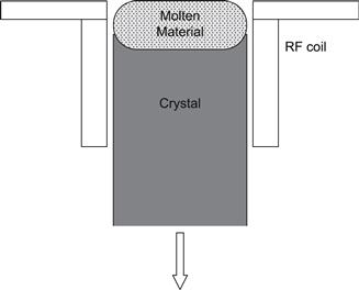
FIGURE 5 Schematic of EMC furnace.
4.4 Float-Zone Silicon
As float-zone silicon typically is used for power electronic components and detectors, the advantage of using large-diameter substrates has been limited, and even today the majority of all float-zone crystals are only 100–125 mm in diameter, which is advantageous for the PV industry needs. Most product and process optimisation activities have been focused on achieving highly predictable yields when running many small series of different types, constantly varying with respect to crystalline orientation (or), diameter (25–150 mm), dopant type (n- or p-type), and resistivity range (0.01–100,000 Ω cm).
During the float-zone growth method, a molten zone is passed along the silicon rod, melting the raw polycrystalline silicon material and leaving behind a purified monocrystal, shown in Figure 6. Modern FZ machines are now capable of accepting feedrods up to 2 m long with a weight between 60 and 100 kg. The bottom end of the feedrod is coned by a grinding operation; during the process, the surface of this cone is heated to the melting temperature of silicon. This results in a thin layer of molten silicon continuously running down the feedrod bottom tip and through the centre hole of the induction coil. The feedrod is heated by a skin current induced by an electromagnetic field. As the feedrod, the molten silicon and the finished crystal are freely suspended in the growth chamber; there is never direct physical contact between silicon and the surroundings except for the ambient gas, typically argon. Contamination is therefore very low, and the process also allows purification of impurities that segregate in the melt.
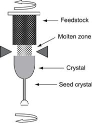
FIGURE 6 Schematic of FZ growth.
As the feed rates of the feedrod and finished crystal can be controlled independently, there are no constraints on the diameter of the monocrystal and the diameter of the feedrod. Typical growth rates of the monocrystal are between 2 and 3 mm/min.
Beside the physical dimension of the monocrystal, the fundamental parameter that must be controlled is the shape of the phase boundaries—i.e., the free surface of the melt and the melt–solid interface where the crystallisation takes place. Factors affecting the phase boundaries are the induction coil current, the pull velocities of the feedrod and monocrystal, the rotation rates, the eccentricity of the rod and monocrystal with respect to the coil centre, and additional heat sources.
The monocrystalline perfection of the finished crystal is very high, as volume defects (precipitates or voids), planar defects (twins grain boundaries or stacking faults), or line defects dislocations) are present. The purity of the finished monocrystal is very high, with oxygen and carbon as the two impurities of highest concentrations (upper limit at 1.0 and 2.0×1016 cm−3, respectively). Also due to the purity of the feedrod material, the concentration of other impurities is very low, and the total concentration of all metal atoms typically lies below 1013 at/cm3 [21,22].
4.5 Nonwafer Technologies
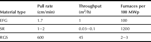
The idea of lowering the wafer manufacturing costs by avoiding the wafer-cutting step with its silicon loss was the main motivation for the development of a number of silicon ribbon-growth technologies. The common feature to all of them is the principle of a continuous production of a thin foil or sheet directly from the silicon melt, using different techniques to confine or stabilise the edges. From these different technologies, developed in R&D programmes such as the JPL flat-plate solar module project [23], only a few are used in commercial wafer production today. The most relevant to date are the edge-defined film fed growth (EFG) [24] (by far the most advanced in terms of industrial performance), the string ribbon (SR) [25], and the dendritic web [26] technology. A great deal of improvement was reported recently in all technologies, and in all cases industrial facilities are described or anticipated. In all cases, tailored cell processing is needed to improve the starting quality of the material, which is generally low. Also, in all cases the technologies appear to be capable of producing very thin sheets, in the 100 μm range. A promising technique from the point of view of productivity is the ribbon-growth on substrate (RGS), originally developed by Bayer with further development at ECN [27].
Other silicon ribbon technologies with the potential for high production rates by decoupling ribbon production from crystal growth (such as the low-angle silicon sheet [LASS] or the supporting web [S-Web]) are not yet developed to industrial production. Table 6 compares production speed and capacity of different silicon ribbon production technologies. The last column shows the number of furnaces for a 100-MWp production line [27].
TABLE 6 Comparison of Different Ribbon Technologies
5 Shaping and Wafering
5.1 Shaping
The large, square-based mc ingots are cut into smaller blocks using large blade or band machines. Blade machines are in general more robust and easy to use and maintain, but they have the disadvantage of producing a relatively high kerf loss, up to 3–4 mm. Band saws, on the other hand, suffer from frequent band breakage and may produce waviness in the blocks, which will then need rectifying. However, modern band saws seem to have greatly improved from this point of view.
Monocrystalline silicon ingots instead are treated as the semiconductor counterpart for removing heads and tails and are shaped to pseudo-square by removing parts of the rounded edges, a process that does not present particular problems, thanks to the relatively small dimension of the ingots.
In the case of mc-Si blocks, it is after the shaping step that blocks are inspected for minority-carrier lifetime and resistivity, as described earlier, so finally tops and tails can be removed to leave the material ready to be wafered.
5.2 Wafering
Wafering of Si ingots for the PV industry is probably one of the only examples of technology successfully transferred to the semiconductor industry, which was originally developed for the PV industry. Cost constraints in PV in fact imposed the development of a slicing technique able to reduce kerf loss and increase productivity, as an alternative to slow, large kerf-loss blade-cutting techniques used until about 10 years ago [15]. On the other hand, the specifications for semiconductor-grade wafers up to 300 mm in diameter needed a totally new concept of machines for the control of taper, thickness variation, and surface smoothness, so at the end both industries enjoy the development of wire-saw technology.
Modern slicing technology is based on wire sawing, where a thin wire (160 μm diameter) web pushes an abrasive-based slurry into the silicon to be cut. In this way, several wafers are cut at the same time, with high mechanical precision and in a highly automated process.
The principle of wire sawing is shown in Figure 7. A spool of single bronze-coated stainless steel wire up to several hundreds of kilometres long (!) is fed on high-precision grooved wire guides. The feeding system, not detailed in the figure, is designed to allow high-precision control of the wire tension, one of the critical parameters of the process, throughout the cut. The silicon block, or blocks, is glued on a low-cost glass support, which in turn is mounted on a motor-driven table that translates downward through the web. The abrasive slurry is fed to the wire web through a nozzle and allows the silicon to be cut. The abrasive is fine-mesh silicon carbide powder. The process is completed when the wires reach the glass, thus allowing the wafers to be separated without any damage as they are attached to the support through a very thin layer of glue. Wire speed and tension, table speed, slurry viscosity and temperature, and abrasive characteristics are the main parameters to control in order to produce wafers that match the specifications indicated in an earlier paragraph. As the conditions tend to change during the process—e.g., because of the increase of the temperature of the slurry or because of the contamination of the slurry by the silicon dust produced by the process—it is critical to be able to adjust the parameters to avoid waves or thickness variations. The slurry can be based on oil or on other fluids that are water washable and can improve subsequent cleaning and handling steps, although the waste-treatment system tends to be more sophisticated than with oil-based procedures, needing for example an oxygen demand control device.
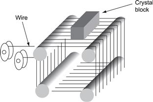
FIGURE 7 Principle of wire sawing.
Typical parameters for cutting 125-mm square wafers over a length of about 30 cm are given in Table 7.
TABLE 7 Typical Watering Conditions Tor 350 μm Thick, 125 mm Square mc-Si Wafers
| Parameter | Value |
| Wire speed (m/s) | 5–10 |
| Table speed (μm/min) | 300–400 |
| Wire diameter (μm) | 160–180 |
| Wire guide pitch (μm) | 550–570 |
| SiC mesh | 500–600 |
| Slurry temperature (°C) | 25±5 |
| Slurry mixture | 1:1 (glycol based) |
| 5:8 (oil based) | |
| Viscosity (g/l) | 1600 |
| Wire tension (N) | 23–25 |
Large wafer manufacturers have developed automated washing and handling equipment for the steps following the cutting one.
References
1. Photon International, March 2002.
2. Bruton T. General trends about photovoltaics based on crystalline silicon Proc E-MRS 2001 Spring Meeting, Symposium E on Crystalline Silicon Solar Cells. Sol Energy Mater Sol Cells. 2002;72:3–10.
3. SEMI™ Standard M61000—SEMI™ International Standards www.semi.org.
4. Ferrazza F. New developments and industrial perspectives of crystalline silicon technologies for PV. Proc. 13th European Photovoltaic Solar Energy Conf., Nice 1995; p. 3.
5. Ferrazza F, et al. The status of crystalline silicon modules. Florence: World Renewable Energy Conf.; 1998;.
6. Kunst H, Beck G. The study of charge carrier kinetics in semiconductors by microwave conductivity measurements. J Appl Phys. 1986;60(10):3558.
7. Schonecker A, et al. Results of five solar silicon wafer minority carrier lifetime round robins organised by the SEMI M6 Solar Silicon Standardisation Task Force. Barcelona: Proc. 14th European Photovoltaic Solar Energy Conf.; 1997; p. 666.
8. Semilab homepage www.semilab.hu.
9. Ferrazza F, et al. Cost effective solar silicon technology. Vienna: Proc. 2nd World Conference on Photovoltaic Solar Energy Conversion; 1998; p. 1220.
10. Endroes A. Mono- and tri-crystalline Si for PV application, Proc E-MRS 2001 Spring Meeting, Symposium E on Crystalline Silicon Solar Cells. Sol Energy Mater Sol Cells. 2002;vol. 72:109–124.
11. Maurits J. Policrystalline Silicon-World Demand and Supply. Colorado: Eighth NREL Workshop on Crystalline Silicon Solar Cell Materials and Processes; 1998.
12. Woditsch F, Koch W. Solar grade silicon feedstock supply for PV industry, Proc E-MRS 2001 Spring Meeting, Symposium E on Crystalline Silicon Solar Cells. Sol Energy Mater Sol Cells. 2002;vol. 72:11–26.
13. Aulich H, Schulze F. Crystalline silicon feedstock for solar cells. Prog Photovolt: Res Appl. 2002;10:141–147.
14. O’Mara W, Herring R, Hunt L, eds. Handbook of Semiconductor Silicon Technology. Noyes Publication 1990.
15. Jester T. Crystalline silicon manufacturing progress. Prog Photovolt: Res Appl. 2002;10:99–106.
16. Ferrazza F. Growth and Post growth Processes of multicrystalline silicon for photovoltaic use. In: Pizzini S, Strunk HP, Werner JH, eds. Polycrystalline Semiconductors IV—Physics, Chemistry and Technology, in Solid State Phenomena. 1995;449–460. Transtec, Switzerland vols. 51–52.
17. Ferrazza F. Large size multicrystalline silicon ingots Proc E-MRS 2001 Spring Meeting, Symposium E on Crystalline Silicon Solar Cells. Sol Energy Mater Sol Cells. 2002;vol. 72:77–81.
18. Franke D, et al. Silicon ingot casting: process development by numerical simulations, Proc E-MRS 2001 Spring Meeting, Symposium E on Crystalline Silicon Solar Cells. Sol Energy Mater Sol Cells. 2002;vol. 72:83–92.
19. Durand F. Electromagnetic continuous pulling process compared to current casting processes with respect to solidification characteristics, Proc of the E-MRS 2001 Spring Meeting, Symposium E on Crystalline Silicon Solar Cells. Sol Energy Mater Sol Cells. 2002;72:125–132.
20. Perichaud I, Martinuzzi S, Durand F. Multicrystalline silicon prepared by electromagnetic continuous pulling: recent results and comparison to directional solidification material. Sol Energy Mater Sol Cells. 2002;72:101–107.
21. W. Dietze, W. Keller, A. Muhlbauer, Float-zone grown silicon, in Crystals, Growth, in: Properties, and Applications, vol. 5, Silicon, Springer-Verlag, 1981, p. 1.
22. Luedge A, Riemann H, Hallmann B, et al. High-speed growth of FZ silicon for photovoltaics. Philadelphia: Proc. High Purity Silicon VII, Electrochemical. Society; 2002.
23. Flat plate solar array project: vol III Silicon sheet: wafers and ribbons. Report DOE/JPL-1012–125 1986.
24. Kaleis J. Silicon ribbons and foils—state of the art, Proc E-MRS 2001 Spring Meeting, Symposium E on Crystalline Silicon Solar Cells. Sol Energy Mater Sol Cells. 2002;vol. 72:139–153.
25. Hanoka J. PVM at contribution towards Evergreen Solar’s new factory. New Orleans: Proc. 29th IEEE Photovoltaic Specialists Conference; 2002; p. 66.
26. Meyer DL, et al. Production of thin (70–100mm) crystalline silicon cells for conformable modules. New Orleans: Proc. 29th IEEE Photovoltaic Specialists Conference; 2002; p. 110.
27. Schonecker A, et al. Ribbon growth-on-substrate: progress in high speed crystalline silicon wafer manufacturing. New Orleans: Proc. 29th IEEE Photovoltaic Specialists Conf.; 2002; p. 316.