
Chapter IC-3
Cu(In,Ga)Se2 Thin-Film Solar Cells
Chapter Outline
2.4. Defect Physics of Cu(In,Ga)Se2
3.1. Structure of the Heterojunction Solar Cell
3.2. Key Elements for High-Efficiency Cu(In,Ga)Se2 Solar Cells
3.3. Absorber Preparation Techniques
3.3.2. Co-Evaporation Processes
3.3.4. Other Absorber Deposition Processes
3.3.5. Postdeposition Air Anneal
3.4.1. The Free Cu(In,Ga)Se2 Surface
3.4.2. Buffer Layer Deposition
3.4.3. Window Layer Deposition
3.5. Module Production and Commercialisation
3.5.1. Monolithic Interconnections
3.5.5. Radiation Hardness and Space Applications
1 Introduction
With a power conversion efficiency of 18.8% on a 0.5-cm2 laboratory cell [1] and 16.6% for mini-modules with an area of around 20 cm2 [2], Cu(In,Ga)Se2 is established as an efficient thin-film solar cell technology. The start of production at several places provides a new challenge for research on this material. However, these recent achievements are based on a long history of research and technological development.
CuInSe2 was synthesised for the first time by Hahn in 1953 [3]. In 1974, this material was proposed as a photovoltaic material [4] with a power conversion efficiency of 12% for a single-crystal solar cell. In the years 1983–84, Boeing Corp. reported efficiencies in excess of 10% from thin poly crystalline films obtained from a three-source co-evaporation process [5]. In 1987 Arco Solar achieved a long-standing record efficiency for a thin-film cell of 14.1% [6]. It took a further ten years, before Arco Solar, at that time Siemens Solar Industries (now Shell Solar), entered the stage of production. In 1998, the first commercial Cu(In,Ga)Se2 solar modules were available [7]. In parallel, a process which avoids the use of H2Se is being developed by Shell Solar in Germany [8] (see also Chapter IV-1). Other companies in the USA, Global Solar and ISET, plan to commercialise modules prepared on other than glass substrates. In Europe, the long-term development efforts of the EUROCIS consortium on the co-evaporation process resulted in the activity of Würth Solar with pilot production envisaged in 2003 [9,10]. In Japan, two lines for film preparation are planned by Showa Shell (selenisation by H2Se) [11] and Matshushita (co-evaporation) [12].
In this chapter, we give a short overview on the present knowledge of Cu(In,Ga)Se2-based heterojunction thin film solar cells. We focus on four points: (i) The description of the basic material properties such as crystal properties, phase diagram, and defect physics. (ii) Description of the cell technology starting from the growth of the polycrystalline Cu(In,Ga)Se2 absorber up to device finishing by heterojunction formation and window layer deposition. This section also discusses basic technologies for module production. (iii) The electronic properties of the finished heterostructure. (iv) Finally, Section 5 discusses the photovoltaic potential of wide-gap chalcopyrites, namely CuGaSe2 and CuInS2, as well as that of the pentenary alloy system Cu(In,Ga)(S,Se)2 and the possibility of building graded-gap structures with these alloys.
This chapter can only briefly cover those scientific issues that are relevant for photovoltaic applications. More detailed information can be found in two review articles by the present authors [13,14] as well as in references [15–19].
2 Material Properties
2.1 Chalcopyrite Lattice
CuInSe2 and CuGaSe2, the materials that form the alloy Cu(In,Ga)Se2, belong to the semiconducting I–III–VI2 materials family that crystallise in the tetragonal chalcopyrite structure. The chalcopyrite structure of, for example, CuInSe2 is obtained from the cubic zinc blende structure of II–VI materials like ZnSe by occupying the Zn sites alternately with Cu and In atoms. Figure 1 compares the two unit cells of the cubic zinc blend structure with the chalcopyrite unit cell. Each I (Cu) or III (In) atom has four bonds to the VI atom (Se). In turn each Se atom has two bonds to Cu and two to In. Because the strengths of the I–VI and III–VI bonds are in general different, the ratio of the lattice constants c/a is not exactly two. Instead, the quantity 2–c/a (which is −0.01 in CuInSe2, +0.04 in CuGaSe2) is a measure of the tetragonal distortion in chalcopyrite materials.

FIGURE 1 Unit cells of chalcogenide compounds. (a) Sphalerite or zinc blende structure of ZnSe (two unit cells); (b) chalcopyrite structure of CuInSe2. The metal sites in the two unit cells of the sphalerite structure of ZnSe are alternately occupied by Cu and In in the chalcopyrite structure.
2.2 Band-Gap Energies
The system of copper chalcopyrites Cu(In,Ga,Al)(Se,S)2 includes a wide range of band-gap energies Eg from 1.04 eV in CuInSe2 up to 2.4 eV in CuGaS2. and even 2.7 eV in CuAIS2, thus, covering most of the visible spectrum. All these compounds have a direct band gap, making them suitable for thin film photovoltaic absorber materials. Figure 2 summarises lattice constants a and band-gap energies Eg of this system. Any desired alloys between these compounds can be produced as no miscibility gap occurs in the entire system. We will discuss the status and prospects of this system in Section 5 in more detail.
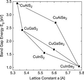
FIGURE 2 Band-gap energies Eg versus the lattice constant a of the Cu(In,Ga,Al)(S,Se)2 alloy system.
2.3 The Phase Diagram
Compared with all other materials used for thin-film photovoltaics, Cu(In,Ga)Se2 has by far the most complicated phase diagram. Figure 3 shows the phase diagram of CuInSe2 given by Haalboom et al. [20]. This investigation had a special focus on temperatures and compositions relevant for the preparation of thin-films. The phase diagram in Figure 3 shows the four different phases which have been found to be relevant in this range: the α-phase (CuInSe2), the β-phase (CuIn3Se5), the δ-phase (the high-temperature sphalerite phase) and CuySe. An interesting point is that all neighbouring phases to the α-phase have a similar structure. The β-phase is actually a defect chalcopyrite phase built by ordered arrays of defect pairs (Cu vacancies VCu and In–Cu antisites InCu). Similarly, CuySe can be viewed as constructed from the chalcopyrite by using Cu–In antisites Culn and Cu interstitials Cui. The transition to the sphalerite phase arises from disordering the cation (Cu, In) sub-lattice, and leads back to the zinc blende structure (cf. Figure 1 (a)).

FIGURE 3 Quasi-binary phase diagram of CuInSe2 along the tie-line that connects the binary compounds In2Se3 and Cu2Se established by Differential Thermal Analysis (DTA) and microscopic phase analysis (After Haalboometal. [20]). Note that at 25 at.% Cu no single phase exists.
The existence range of the α-phase in pure CuInSe2 on the quasi-binary tie line Cu2Se-In2Se3 extends from a Cu content of 24 to 24.5 at.%. Thus, the existence range of single-phase CuInSe2 is relatively small and does not even include the stoichiometric composition of 25 at.% Cu. The Cu content of absorbers for thin-film solar cells varies typically between 22 and 24 at.% Cu. At the growth temperature this compositional range lies within the single-phase region of the α-phase. However, at room temperature it lies in the two-phase α+β region of the equilibrium phase diagram [20]. Hence one would expect a tendency for phase separation in photovoltaic-grade CuInSe2 after deposition. Fortunately, it turns out that partial replacement of In with Ga, as well as the use of Na-containing substrates, considerably widens the single-phase region in terms of (In+Ga)/(In+Ga+Cu) ratios [21]. Thus, the phase diagram hints at the substantial improvements actually achieved in recent years by the use of Na-containing substrates, as well as by the use of Cu(In,Ga)Se2 alloys.
2.4 Defect Physics of Cu(In,Ga)Se2
The defect structure of the ternary compounds CuInSe2, CuGaSe2, CuInS2, and their alloys, is of special importance because of the large number of possible intrinsic defects and the role of deep recombination centres for the performance of the solar cells. The features that are somewhat special to the Cu-chalcopyrite compounds are the ability to dope these compounds with native defects, their tolerance to large off-stoichiometries, and the electrically neutral nature of structural defects in these materials. It is obvious that the explanation of these effects significantly contributes to the explanation of the photovoltaic performance of these compounds. Doping of CuInSe2 is controlled by intrinsic defects. Samples with p-type conductivity are grown if the material is Cu-poor and annealed under high Se vapour pressure, whereas Cu-rich material with Se deficiency tends to be n-type [22,23]. Thus, the Se vacancy VSe is considered to be the dominant donor in n-type material (and also the compensating donor in p-type material), and the Cu vacancy VCu the dominant acceptor in Cu-poor p-type material.
By calculating the metal-related defects in CuInSe2 and CuGaSe2, Zhang et al. [24] found that the defect formation energies for some intrinsic defects are so low that they can be heavily influenced by the chemical potential of the components (i.e., by the composition of the material) as well as by the electrochemical potential of the electrons. For VCu in Cu-poor and stoichiometric material, a negative formation energy is even calculated. This would imply the spontaneous formation of large numbers of these defects under equilibrium conditions. Low (but positive) formation energies are also found for the antisite CuIn in Cu-rich material (this defect is a shallow acceptor which could be responsible for the p-type conductivity of Cu-rich, non-Se-deficient CuInSe2). The dependence of the defect formation energies on the electron Fermi level could explain the strong tendency of CuInSe2 to self-compensation and the difficulties of achieving extrinsic doping. The results of Zhang et al. [24] provide a good theoretical model of defect formation energies and defect transition energies, which exhibits good agreement with experimentally obtained data. Table 1 summarises the ionisation energies and the defect formation energies of the 12 intrinsic defects in CuInSe2. The energies (bold values in Table 1) for VCu. VIn, CuI, CuIn, InCu, are obtained from a first principle calculation [24] whereas the formation energies in italics (Table 1) and for the other defects are calculated from the macroscopic cavity model [25]. The ionisation energies used in Table 1 are either taken from Zhang et al. [24] or from the data compiled in reference [26]. Note that the data given in references [25,26] for the cation defects differ significantly from those computed in reference [24].
TABLE 1 Electronic Transition Energies and Formation Energies ΔU of the 12 Intrinsic Defects in CuInSe2

Source: the Ionisation Energies in Italics are Derived from Reference [26], and the Formation Energies in Italics are from Reference [25]. All the Numbers in Bold Type are from Reference [24].
aDifference between the valence/conduction band energy for acceptor/donor states.
bFormation energy ΔU of the neutral defect in the stoichiometric material.
Further important results in reference [24] are the formation energies of defect complexes such as (2VCu, InCu). (CuIn, InCu) and (2CuI, CuIn), where CuI is an interstitial Cu atom. These formation energies are even lower than those of the corresponding isolated defects. Interestingly, the (2VCu, InCu) complex does not exhibit an electronic transition within the forbidden gap, in contrast to the isolated InCu-anti-site, which is a deep recombination centre. As the (2VCu, InCu) complex is most likely to occur in In-rich material, it can accommodate a large amount of excess In (or likewise deficient Cu) and, at same time, maintain the electrical performance of the material. Furthermore, ordered arrays of this complex can be thought as the building blocks of a series of Cu-poor Cu–In–Se compounds such as CuIn5Se5 and CuIn5Se8 [24].
Let us now concentrate on the defects experimentally detected in photovoltaic grade (and thus In-rich) polycrystalline films. In-rich Cu(In,Ga)Se2 is in general highly compensated, with a net acceptor concentration of the order of 1016 cm−3. The shallow acceptor level VCu (which lies about 30 meV above the valence band) is assumed to be the main dopant in this material. As compensating donors, the Se-vacancy VSe as well as the double donor InCu are considered. The most prominent defect is an acceptor level at about 270–300 meV above the valence band, which is reported by several groups from deep-level transient spectroscopy [27] and admittance spectroscopy [28,29]. This defect is also present in single crystals [30]. The importance of this transition results from the fact that its concentration is related to the open-circuit voltage of the device [31–33]. Upon investigating defect energies in the entire Cu(In,Ga)(Se,S)2 alloy system, Turcu et al. [34] found that the energy distance between this defect and the valence band maximum remains constant when alloying CuInSe2 with Ga, whereas the energy distance increases under S/Se alloying. Assuming that the defect energy is independent from the energy position of the band edges, like the defect energies of transition metal impurities in III–V and II–IV semiconductor alloys [35,36], the authors of reference [34] extrapolate the valence band offsets ΔEv = −0.23 eV for the combination CuInSe2/CuInS2 and ΔEv = 0.04 eV for CuInSe2/CuGaSe2. Recently, transient photocapacitance studies by Heath et al. [37] unveiled an additional defect state in Cu(In,Ga)Se2 at about 0.8 eV from the valence band. Again, the defect energy is independent of the Ga content in the alloy. Figure 4 summarises the energy positions of bulk defects in the Cu(In1−xGax)Se2 and the CuIn(Se1−ySy)2 alloy system with the defect energy of the bulk acceptor used as a reference energy to align the valence and conduction band energy [38]. Additionally, Figure 4 shows the activation energy of an interface donor. This energy corresponds to the energy difference ΔEFn between the Fermi energy and the conduction band minimum at the buffer absorber interface [39]. Notably this energy difference remains small upon alloying CuInSe2 with Ga, whereas ΔEFn increases when alloying with S.
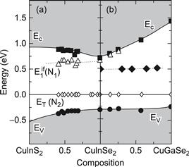
FIGURE 4 Band gap evolution diagram of the CuIn(Se,S)2 (a) and the Cu(In,Ga)Se2 (b) alloy system with the trap energy ET(N2, open diamonds) taken as an internal reference to align the conduction band and the valence band energies Ec and Ev. The energy position of an additional defect state in Cu(In,Ga)Se2 (full diamonds) as well as that of an interface donor (open triangles) in Cu(In,Ga)(Se,S)2 is also indicated.
3 Cell and Module Technology
3.1 Structure of the Heterojunction Solar Cell
The complete layer sequence of a ZnO/CdS/Cu(In,Ga)Se2 heterojunction solar cell is shown in Figure 5. The device consists of a typically 1-μm-thick Mo layer deposited on a soda-lime glass substrate and serving as the back contact for the solar cell. The Cu(In,Ga)Se2 is deposited on top of the Mo back electrode as the photovoltaic absorber material. This absorber layer has a thickness of 1–2 μm. The heterojunction is then completed by chemical bath deposition (CBD) of CdS (typically 50 nm thick) and by the sputter deposition of a nominally undoped (intrinsic) i-ZnO layer (usually of thickness 50–70 nm) and then a heavily doped ZnO layer. As ZnO has a band-gap energy of 3.2 eV it is transparent for the main part of the solar spectrum and therefore is denoted as the window layer of the solar cell.
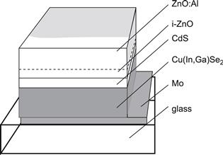
FIGURE 5 Schematic layer sequence of a standard ZnO/CdS/Cu(In,Ga)Se2 thin-film solar cell.
3.2 Key Elements for High-Efficiency Cu(In,Ga)Se2 Solar Cells
We first mention four important technological innovations which, during the decade 1990–2000, have led to a considerable improvement of the efficiencies and finally to the record efficiency of 18.8% [1]. These steps are the key elements of the present Cu(In,Ga)Se2 technology:
• The film quality has been substantially improved by the crystallisation mechanism induced by the presence of CuySe (y < 2). This process is further supported by a substrate temperature close to the softening point of the glass substrate [40].
• The glass substrate has been changed from Na-free glass to Na-containing soda-lime glass [40,41]. The incorporation of Na, either from the glass substrate or from Na-containing precursors, has led to an enormous improvement of the efficiency and reliability of the solar cells, as well as to a larger process tolerance.
• Early absorbers consisted of pure CuInSe2. The partial replacement of In with Ga [42] is a further noticeable improvement, which has increased the band gap of the absorber from 1.04 eV to 1.1–1.2 eV for the high-efficiency devices. The benefit of 20–30% Ga incorporation stems not only from the better band gap match to the solar spectrum but also from the improved electronic quality of Cu(In,Ga)Se2 with respect to pure CuInSe2 [21,32].
• The counter electrode for the CuInSe2 absorber of the earlier cells was a 2 μm thick CdS layer deposited by Physical Vapour Deposition (PVD). This has been replaced by a combination of a 50-nm-thin CdS buffer layer laid down by chemical bath deposition [43,44] and a highly conductive ZnO window layer.
3.3 Absorber Preparation Techniques
3.3.1 Basics
The preparation of Cu(In,Ga)Se2-based solar cells starts with the deposition of the absorber material on a Mo-coated glass substrate (preferably soda-lime glass). The properties of the Mo film and the choice of the glass substrate are of primary importance for the final device quality, because of the importance of Na, which diffuses from the glass through the Mo film into the growing absorber material. In the past, some processes used blocking layers such as SiNx, SiO2, or Cr between the glass substrate and the Mo film to prevent the out-diffusion of Na. Instead, Na-containing precursors like NaF [45], Na2Se [46], or Na2S [47] are then deposited prior to absorber growth to provide a controlled, more homogeneous, incorporation of Na into the film. The control of Na incorporation in the film from precursor layers allows the use of other substrates like metal or polymer foils. The most obvious effects of Na incorporation are better film morphology and higher conductivity of the films [48]. Furthermore, the incorporation of Na induces beneficial changes in the defect distribution of the absorber films [49,50].
The explanations for the beneficial impact of Na are manifold, and it is most likely that the incorporation of Na in fact results in a variety of consequences. During film growth, the incorporation of Na leads to the formation of NaSex compounds. This slows down the growth of CuInSe2 and could at same time facilitate the incorporation of Se into the film [51]. Also the widening of the existence range of the α-(CuInSe2) phase in the phase diagram, discussed above, as well as the reported larger tolerance to the Cu/(In+Ga) ratio of Na-containing thin films, could be explained in this picture. Furthermore, the higher conductivity of Na-containing films could result from the diminished number of compensating Vse donors.
During absorber deposition, a MoSe2 film forms at the Mo surface [52,53]. MoSe2 is a layered semiconductor with p-type conduction, a band gap of 1.3 eV and weak van der Waals bonding along the c-axis. The c-axis is found to be in parallel with, and the van der Waals planes thus perpendicular to, the interface [53]. Because of the larger band gap of the MoSe2 compared with that of standard Cu(In,Ga)Se2 films, the MoSe2 layer provides a low-recombinative back surface for the photogenerated minority carriers (electrons) in the Cu(In,Ga)Se2 absorber and at the same time provides a low-resistance contact for the majority carries (holes).
Photovoltaic-grade Cu(In,Ga)Se2 films have a slightly In-rich overall composition. The allowed stoichiometry deviations are astonishingly large, yielding a wide process window with respect to composition. Devices with efficiencies above 14% are obtained from absorbers with (In+Ga)/(ln+Ga+Cu) ratios between 52% and 64% if the sample contains Na [48]. Cu-rich Cu(In,Ga)Se2 shows the segregation of a secondary CuySe phase preferentially at the surface of the absorber film. The metallic nature of this phase does not allow the formation of efficient heterojunctions. Even after removal of the secondary phase from the surface by etching the absorber in KCN, the utility of this material for photovoltaic applications is limited. However, the importance of the Cu-rich composition is given by its role during film growth. Cu-rich films have grain sizes in excess of 1 μm whereas In-rich films have much smaller grains. A model for the film growth under Cu-rich compositions comprises the role of CuySe as a flux agent during the growth process of co-evaporated films [54]. For Cu(In,Ga)Se2 prepared by selenisation, the role of CuySe is similar [55]. Therefore, growth processes for high quality material have to go through a copper-rich stage but have to end up with an indium-rich overall composition.
3.3.2 Co-Evaporation Processes
The absorber material yielding the highest efficiencies is Cu(In,Ga)Se2 with a Ga/(Ga + In) ratio of 20–30%, prepared by co-evaporation from elemental sources. Figure 6 sketches a co-evaporation set-up as used for the preparation of laboratory-scale solar cells and mini-modules. The process requires a maximum substrate temperature of about 550 °C for a certain time during film growth, preferably towards the end of growth. One advantage of the evaporation route is that material deposition and film formation are performed during the same processing step. A feedback loop based on a quadrupole mass spectrometer or an atomic absorption spectrometer controls the rates of each source. The composition of the deposited material with regard to the metals corresponds to their evaporation rates, whereas Se is always evaporated in excess. This precise control over the deposition rates allows for a wide range of variations and optimisations with different sub-steps or stages for film deposition and growth. These sequences are defined by the evaporation rates of the different sources and the substrate temperature during the course of deposition.
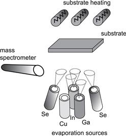
FIGURE 6 Arrangement for the deposition of Cu(In,Ga)Se2 films on the laboratory scale by co-evaporation on a heated substrate. The rates of the sources are controlled by mass spectrometry.
Advanced preparation sequences always include a Cu-rich stage during the growth process and end up with an In-rich overall composition in order to combine the large grains of the Cu-rich stage with the otherwise more favourable electronic properties of the In-rich composition. The first example of this kind of procedure is the so called Boeing or bilayer process [5], which starts with the deposition of Cu-rich Cu(In,Ga)Se2 and ends with an excess In rate. The most successful co-evaporation process is the so-called three-stage process [56]. This process starts with the deposition of In,Ga, and Se at relatively low temperatures, then uses a Cu-rich growth stage by evaporating Cu in excess at elevated temperature, and at the end again deposits only In, Ga, and Se to ensure the overall In-rich composition of the film. The three-stage process currently leads to the Cu(In,Ga)Se2 solar cells with the highest efficiencies.
3.3.3 Selenisation Processes
The second class of absorber preparation routes is based on the separation of deposition and compound formation into two different processing steps. High efficiencies are obtained from absorber prepared by selenisation of metal precursors in H2Se [57–59] and by rapid thermal processing of stacked elemental layers in a Se atmosphere [60]. These sequential processes have the advantage that approved large-area deposition techniques like sputtering can be used for the deposition of the materials. The Cu(In,Ga)Se2 film formation then requires a second step, the selenisation.
The very first large-area modules were prepared by the selenisation of metal precursors in the presence of H2Se more than ten years ago [6]. Today, a modification of this process yields the first commercially available Cu(In,Ga)Se2 solar cells manufactured by Shell Solar Industries. This process is schematically illustrated in Figure 7. First, a stacked layer of Cu, In and Ga is sputter-deposited on the Mo-coated glass substrate. Then selenisation takes place under H2Se. To improve the device performance, a second thermal process under H2S is added, resulting in an absorber that is Cu(In,Ga)(S,Se)2 rather than Cu(In,Ga)Se2.
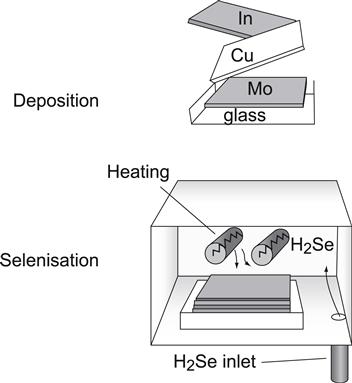
FIGURE 7 Illustration of the sequential process. First a stack of metal (Cu,In,Ga) layers deposited by sputtering onto a Mo-coated glass. In the second step, this slack is selenised in H2Se atmosphere and converted into CuIn Se2.
A variation of the method that avoids the use of the toxic H2Se during selenisation is the rapid thermal processing of stacked elemental layers [60]. Here the precursor includes a layer of evaporated elemental Se. The stack is then selenised by a rapid thermal process (RTP) in either an inert or a Se atmosphere. The highest efficiencies are obtained if the RTP is performed in an S-containing atmosphere (either pure S or H2S).
On the laboratory scale, the efficiencies of cells made by these preparation routes are smaller by about 3% (absolute) as compared with the record values. However, on the module level, co-evaporated and sequentially prepared absorbers have about the same efficiency. Sequential processes need two or even three stages for absorber completion. These additional processing steps may counterbalance the advantage of easier element deposition by sputtering.
3.3.4 Other Absorber Deposition Processes
Besides selenisation and co-evaporation, other deposition methods have been studied, either to obtain films with very high quality or to reduce the cost of film deposition on large areas. Methods that are used to grow epitaxial III–V compound films, such as molecular beam epitaxy (MBE) [61] or metal organic chemical vapour deposition (MOCVD) [62] have revealed interesting features for fundamental studies like phase segregation and defect formation, but could not be used to form the absorber material for high-efficiency solar cells.
Attempts to develop so-called low-cost processes include electrodeposition [63–66], screen printing and particle deposition [67,68]. Electrodeposition can be done either in one or two steps. The crucial step is the final film formation in a high-temperature annealing process. The recrystallisation process competes with the decomposition of the material. Therefore, process optimisation is quite difficult. Cells with high efficiencies were obtained by electrodeposition of a Cu-rich CuInSe2 film and subsequent conditioning by a vacuum evaporation step of In(Se) [69]. Particle deposition by printing of suitable inks and subsequent annealing lead to absorber layers with good quality enabling the fabrication of solar cells with efficiencies over 13% [70].
3.3.5 Postdeposition Air Anneal
Air annealing has been an important process step, crucial for the efficiency especially of the early solar cells based on CuInSe2. Though often not mentioned explicitly, an oxygenation step is still used for most of the present-day high-efficiency devices. The beneficial effect of oxygen was explained within the defect chemical model of Cahen and Noufi [71]. In this model, the surface defects at grain boundaries are positively charged Se vacancies VSe. During air annealing, these sites are passivated by O atoms. Because of the decreased charge at the grain boundary, the band bending as well as the recombination probability for photogenerated electrons is reduced. The surface donors and their neutralisation by oxygen are important for the free Cu(In,Ga)Se2 surface as well as for the formation of the CdS/Cu(In,Ga)Se2 interface [72,73].
3.4 Heterojunction Formation
3.4.1 The Free Cu(In,Ga)Se2 Surface
The surface properties of Cu(In,Ga)Se2 thin films are especially important as this surface becomes the active interface of the completed solar cell. However, the band diagram of the ZnO/CdS/Cu(In,Ga)Se2 heterojunction, especially the detailed structure close to the CdS/Cu(In,Ga)Se2 interface, is still under debate (for recent reviews see references [74,75]).
The free surfaces of as-grown Cu(In,Ga)Se2 films exhibit two prominent features:
1. The valence band-edge energy EV lies below the Fermi level EF by about 1.1 eV for CuInSe2 films [76]. This energy is larger than the band-gap energy Ebulkg of the bulk of the absorber material. This finding was taken as an indication for a widening of band gap at the surface of the film. A recent direct measurement of the surface band gap of polycrystalline CuInSe2 by Morkel et al. [77] proved that the band-gap energy Esurfg at the surface of the film is about 1.4 cV, i.e., more than 0.3 eV larger than Ebulkg≈1.04 eV. In Cu(In1−x,Gax)Se2 alloys the distance EF– EV was found to be 0.8 eV (almost independently of the Ga content if x > 0) [78].
2. The surface composition of Cu-poor CuInSe2, as well as that of Cu(In,Ga)Se2 films, corresponds to a surface composition of (Ga + In)/(Ga + In + Cu) of about 0.75 for a range of bulk compositions of 0.5 < (Ga + In)/(Ga + In + Cu) < 0.75 [76].
Both observations (i) and (ii) have led to the assumption that a phase segregation of Cu(In,Ga)3Se5, the so-called Ordered Defect Compound (ODC), occurs at the surface of the films. From the fact that bulk Cu(In,Ga)3Se5 exhibits n-type conductivity [79] it was argued that Cu-poor Cu(In,Ga)Se2 thin films automatically generate a rectifying, buried junction. However, the existence of a separate phase on top of standard Cu(In,Ga)Se2 thin films has not yet been confirmed by structural methods such as X-ray diffraction, high resolution transmission electron microscopy or electron diffraction. Furthermore, if the surface phase exhibited the weak n-type conductivity of bulk Cu(In,Ga)3Se5, simple charge neutrality estimations [21] show that this would not be sufficient to achieve type inversion.
Based on these arguments, another picture of the surface of Cu(In,Ga)Se2 thin films and of junction formation has emerged [21,80]. Within the classical Bardeen model [81] of Fermi level pinning by electronic states at semiconductor surfaces, a density of surface states of about 1012 cm−2 eV−1 is sufficient to pin the Fermi level at the neutrality level of the free semiconductor surfaces. Positively charged surface donors are expected in the metal terminated (112) surface of CuInSe2 owing to the dangling bond to the missing Se [71]. Thus, these surface states, rather than a distinct n-type surface phase, determine the type inversion of the surface.
Surface states play also an important role in the completed heterostructure, where they become interface states at the absorber/buffer interlace. The deject layer model [21,80] takes into account a modification of the band structure due to the Cu deficiency of the surface as well as the presence of positively charged surface states due to the missing surface Se. However, the defect layer model considers the surface layer not as n-type bulk material (as does the ODC model) but as a p+-layer. Furthermore, the defect layer is viewed not as the origin but rather as the consequence of the natural surface type inversion [21,80]. Surface states are responsible for the surface band bending that leads to the liberation of Cu from its lattice sites and to Cu migration towards the neutral part of the film. The remaining copper vacancies ![]() close to the surface result in a high density of acceptor states, i.e., the p+-defect layer at the film surface. Recent photoelectron spectroscopy experiments of Klein and Jaegermann [82] suggest that the band bending occurring during junction formation leads to a loss of Cu atoms from the surface of CuInSe2 and CuGaSe2, whereas a similar effect was not observed in CuInS2.
close to the surface result in a high density of acceptor states, i.e., the p+-defect layer at the film surface. Recent photoelectron spectroscopy experiments of Klein and Jaegermann [82] suggest that the band bending occurring during junction formation leads to a loss of Cu atoms from the surface of CuInSe2 and CuGaSe2, whereas a similar effect was not observed in CuInS2.
3.4.2 Buffer Layer Deposition
Surface passivation and junction formation is most easily achieved by the CBD deposition of a thin CdS film from a chemical solution containing Cd ions and thiourea [83]. The benefit of the CdS layer is manifold:
• CBD deposition of CdS provides complete coverage of the rough polycrystalline absorber surface at a film thickness of only 10 nm [84].
• The layer provides protection against damage and chemical reactions resulting from the subsequent ZnO deposition process.
• The chemical bath removes the natural oxide from the film surface [83] and thus reestablishes positively charged surface states and, as a consequence, the natural type inversion at the CdS/Cu(In,Ga)Se2 interface.
• The Cd ions, reacting first with the absorber surface, remove elemental Se, possibly by the formation of CdSe.
• The Cd ions also diffuse to a certain extent into the Cu-poor surface layer of the absorber material [85,86], where they possibly form CdCu donors, thus providing additional positive charges enhancing the type inversion of the buffer/absorber interface.
• Open-circuit voltage limitations imposed by interface recombination can be overcome by a low surface recombination velocity in addition to the type inversion of the absorber surface. Thus, one might conclude that interface states (except those shallow surface donors responsible for the type inversion) are also passivated by the chemical bath.
Due to the favourable properties of CdS as a heterojunction partner and the chemistry of the CBD process it is difficult to find a replacement. Avoiding CdS and the chemical bath step would be advantageous from the production point of view. On one hand, a toxic material such as CdS requires additional safety regulation; on the other hand, the chemical bath deposition does not comply with the vacuum deposition steps of an in-line module fabrication. Therefore, research and development in this area relates to two issues: (i) the search for alternative materials for a chemical deposition, and (ii) the development of ways to deposit the front electrode without an intermediate step in a chemical bath.
Promising materials to replace CdS are In(OH,S) [78], Zn(OH,S) [88,89], ZnS [90,91], and ZnSe [92–94], However, all these materials require additional precautions to be taken for the preparation of the absorber surface or front electrode deposition.
3.4.3 Window Layer Deposition
The most commonly used material for the preparation of the front electrode is ZnO doped with B or Al. The first large-area modules produced by ARCO Solar (later Siemens Solar Industries, now Shell Solar Industries) had a ZnO:B window layer deposited by chemical vapour deposition (CVD). Later production facilities at Boeing and EUROCIS use sputtering processes. Present pilot production lines also favour sputtering. As mentioned previously, an undoped i-ZnO layer with a thickness of about 50–100 nm is needed at the heterojunction in order to achieve optimum performance.
3.5 Module Production and Commercialisation
3.5.1 Monolithic Interconnections
One inherent advantage of thin-film technology for photovoltaics is the possibility of using monolithic integration for series connection of individual cells within a module. In contrast, bulk Si solar cells must be provided with a front metal grid, and each of these front contacts has to be connected to the back contact of the next cell for series connection. The interconnect scheme, shown in Figure 8, has to warrant that the front ZnO layer of one cell is connected to the back Mo contact of the next one. In order to obtain this connection, three different patterning steps are necessary. The first one separates the Mo back contact by a series of periodical scribes and thus defines the width of the cells, which is of the order of 0.5–1 cm. For Mo patterning, a laser is normally used. The second patterning step is performed after absorber and buffer deposition, and the final one after window deposition (cf. Figure 8). Scribing of the semiconductor layer is done by mechanical scribing or laser scribing. The total width of the interconnect depends not only on the scribing tools, but also on the reproducibility of the scribing lines along the entire module. The length of the cells and, accordingly, that of the scribes can be more than 1 m. The typical interconnect width is of the order of 300 μm. Thus, about 3–5% of the cell area must be sacrificed to the interconnects.

FIGURE 8 Deposition and patterning sequence to obtain an integrated interconnect scheme for Cu(In,Ga)Se2 thin-film modules.
3.5.2 Module Fabrication
The technologies for absorber, buffer, and window deposition used for module production are the same as those discussed above for the production of small laboratory cells. However, the challenge of producing modules is to transform the laboratory-scale technologies to much larger areas. The selenisation process uses as much off-the-shelf equipment and processing as possible (e.g., sputtering of the metal precursors) for fabricating Cu(In,Ga)Se2 films. For co-evaporation on large areas, the Centre for Solar Energy and Hydrogen Research in Stuttgart (ZSW) has designed its own equipment, schematically shown in Figure 9, for an in-line co-evaporation process. Line-shaped evaporation sources allow continuous deposition of large-area, high-quality Cu(In,Ga)Se2 films. The relatively high substrate temperatures that are necessary for high-quality material impose problems in handling very large area glass sheets. Future process optimisation therefore implies reduction of the substrate temperature.

FIGURE 9 Sketch of an in-line deposition system for co-evaporation of Cu(In,Ga)Se2 absorber films from line-sources.
A bottleneck for the production is the deposition of the buffer layer in a chemical bath. On one hand, it is not straightforward to integrate this process in a line consisting mainly of dry physical vapour deposition processes; on the other, it would be favourable for environmental reasons to replace the currently used CdS layer by a Cd-free alternative.
The ZnO transparent front electrode is put down either by CVD or sputtering. Each method has its specific advantages with respect to process tolerance, throughput, cost and film properties. The widths of the cells within the module—and therefore the relative losses from the patterning—mainly depend on the sheet resistance of the ZnO.
Module encapsulation is an important issue because module stability depends on proper protection against humidity. Low-iron cover glasses provide good protection against ambient influences. Hermetic sealing of the edges is mandatory to obtain stable modules (see the following discussion).
3.5.3 Upscaling Achievements
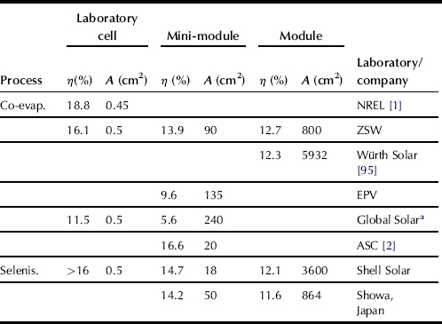
Cu(In,Ga)Se2 has the best potential to reach more than 15% module efficiency in the near future. Mini-modules ranging in area from 20 cm2 to 90 cm2 that use the process sequence anticipated for larger area commercial modules have already reached efficiencies around 14–15%. Recently, Siemens Solar Industries fabricated a 1 ft × 4 ft power module (−44 watts) with an independently verified efficiency of 12.1%. Using a totally different approach to the deposition of the absorber layer, the ZSW fabricated a 30-cm × 30-cm module with a verified efficiency of 12.7%. Based on the same co-evaporation process, Würth Solar GmbH, Stuttgart, reported an efficiency of 12.5% for a module of aperture area 5932 cm2 [95]. More results of the different processes are summarised in Table 2. Note that, because of the promising results from the laboratory scale and the first approaches of up-scaling, several companies other than those mentioned in Table 2 now plan commercial production.
TABLE 2 Comparison of Efficiencies η and Areas A of Laboratory Cells, Mini-Modules, and Commercial-Size Modules Achieved with Cu(In,Ga)Se2 Thin Films Based on the Co-Evaporation and the Selenisation Process. NREL Denotes the National Renewable Energy Laboratories (USA), ZSW is the Center for Solar Energy and Hydrogen Research (Germany), EPV is Energy Photovoltaics (USA), ASC is the Angstrom Solar Centre (Sweden)
A further challenge is to develop CIGS cells on flexible substrates and hence to extend their area of applications. There are ongoing efforts to produce cells on various kinds of substrates like stainless steel, polymide and at the same time to retain the performance achieved with devices on soda-lime glass [96]. For space applications it is important to reduce the weight by depositing the cells on lightweight foil substrates. Highest small-area efficiencies on polymide films formed by spin coating on a glass substrate reach 12.8% [97]. Roll to roll coating on metal foils [98] and polymer films [99,100] has already reached the stage of pilot production.
3.5.4 Stability
The long-term stability is a critical issue of any solar cell technology because the module lifetime contributes as much to the ratio between produced energy and invested cost as does the initial efficiency. Cu(In,Ga)Se2 modules fabricated by Shell Solar Industries more than 10 years ago show until today very good stability during outdoor operation [101,102]. However, intense accelerated lifetime testing is made for the now commercially available Cu(In,Ga)Se2 modules. Careful sealing and encapsulation appears mandatory, especially because of the sensitivity of Cu(In,Ga)Se2 to humidity. For non-encapsulated modules, corrosion of the molybdenum contact and the degradation of zinc oxide were found to be the dominating degradation mechanisms [103] during the so-called damp heat test (1000 hours in hot (85 °C) and humid (85% humidity) atmosphere). Investigations of non-encapsulated cells [104–106] unveiled further a humidity-induced degradation of the Cu(In,Ga)Se2 absorber material. Despite of the sensibility of Cu(In,Ga)Se2 with respect to humidity, well encapsulated modules pass the damp heat test [107].
Recent work of Guillemoles et al. [108,109] investigates the chemical and electronic stability of Cu(In,Ga)Se2-based solar cells and possible fundamental instabilities of the material system, namely, interface reactions, defect metastability, and constituent element (Cu) mobility. Guillemoles et al. conclude that all reasonably anticipated detrimental interface reactions at the Mo/Cu(In,Ga)Se2, the Cu(In,Ga)Se2/CdS. or the CdS/ZnO interface are either thermodynamically or kinetically limited, Furthermore, Cu mobility does not contradict long-term stability [108,109].
3.5.5 Radiation Hardness and Space Applications
One important prospective application for Cu(In,Ga)Se2 cells is in space, where the main power source is photovoltaics. Satellites in low-earth orbits for communication systems require solar cells with high end-of-life efficiencies, despite the high flux of high-energy electrons and protons in that ambient. The radiation hardness of Cu(In,Ga)Se2 has been recognized as early as 1984/85 [110,111], but only recently have systematic investigations on the radiation response of Cu(In,Ga)Se2 solar cells been undergone using high enough electron and proton fluences to allow quantitative conclusions regarding the defect generation rates [112]. The radiation resistance of Cu(In,Ga)Se2 against high-energy (0.3–3 MeV) electrons turns out to be far better than that of any other photovoltaic material [112]. The radiation hardness of Cu(In,Ga)Se2 against high-energy (0.4–10 MeV) protons is also high, though the difference from other materials is not as high as in case of electron irradiation. Walters et al. [113] have analysed Cu(In,Ga)Se2 in the frame of the so-called damage dose model and found that the damage coefficients for Cu(In,Ga)Se2 are comparable to those of InP and considerably smaller than those of Si and GaAs.
The high mobility of Cu in the Cu(In,Ga)Se2 lattice was proposed to be one important ingredient for a defect healing mechanism that could explain the high radiation resistance of Cu(In,Ga)Se2 [108,114]. Recent thermal annealing experiments of electron-irradiated [115] and proton-irradiated [116] Cu(In,Ga)Se2 solar cells unveiled a thermally activated healing process with an activation energy of around 1 cV leading to a complete recovery of the device performance. Illumination of the solar cell enhances this annealing process further [116,117].
The challenge for developing CIGS space cells is to reduce the weight by depositing the cells on foil substrates, and at the same time to retain the performance achieved with devices on soda-lime glass. Recently, Tuttle et al. [118] reported a Cu(In,Ga)Se2 solar cell on lightweight metal foil with a power conversion efficiency of 15.2% (under AM0 illumination) and a specific power of 1235 W/kg. Other approaches to flexible and lightweight Cu(In,Ga)Se2 solar cells embrace Cu(In,Ga)Se2 deposited on plastic foil such as polyimide [119] or the use of a lift-off technique to remove the absorber from the glass substrate after device fabrication [120].
4 Device Physics
4.1 The Band Diagram
The band diagram of the ZnO/CdS/Cu(In,Ga)Se2 heterostructure in Figure 10 shows the conduction and valence band energies Ec and Ev of the Cu(In,Ga)Se2 absorber, the CdS buffer layer and the ZnO window. Note that the latter consists of a highly Al-doped (ZnO:Al) and an undoped (i-ZnO) layer. For the moment, we neglect the polycrystalline nature of the semiconductor materials, which in principle requires a two- or three-dimensional band diagram. Even in the one-dimensional model, important details of the band diagram are still not perfectly clear. The diagram in Figure 10 concentrates on the heterojunction and does not show the contact between the Mo and Cu(In,Ga)Se2 at the back side of the absorber.
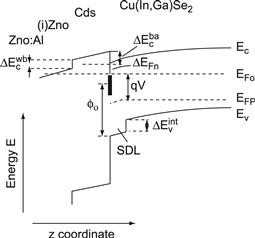
FIGURE 10 Band diagram of the ZnO/CdS/Cu(In,Ga)Se2 heterojunction under bias voltage showing the conduction and valence band-edge energies ΔEc and Ev. The quantities ΔEcwb/ba denote the conduction band offsets at the window/buffer and buffer/absorber interfaces, respectively. An internal valence band offset ΔEvint exists between the bulk Cu(In,Ga)Se2 and a surface defect layer (SDL) on top of the Cu(In,Ga)Se2 absorber film. The quantity ΔEFn denotes the energy distance between the electron Fermi level EFn and the conduction band at the CdS buffer/Cu(In,Ga)Se2 absorber interface, and ϕn denotes the neutrality level of interface states at this heterointerface.
An important feature in Figure 10 is the 10–30-nm-thick surface defect layer (SDL) on top of the Cu(In,Ga)Se2 absorber, already discussed in Section 3.4. The physical nature of this SDL is still under debate. However, the fact that the band gap at the surface of Cu(In,Ga)Se2 thin films (as long as they are prepared with a slightly Cu-poor final composition) exceeds the band-gap energy of the bulk material [76,77], has important implications for the contribution of interface recombination to the overall performance of the solar cell. A simplified approach to the mathematical description of the ZnO/CdS/Cu(In,Ga)Se2 heterojunction including the consequence of the surface-band-gap widening is given in reference [121].
The most important quantities to be considered in the band diagram are the band discontinuities between the different heterojunction partners. Band discontinuities in terms of valence band offsets ΔI between semiconductor a and b are usually determined by photoelectron spectroscopy (for a discussion with respect to Cu-chalcopyrite surfaces and interfaces, see [74]). The valence band offset between a (011)-oriented Cu(In,Ga)Se2 single crystal and CdS deposited by PVD at room temperature is determined as [122,123] ΔE abv = −0.8 (±0.2) eV (and, therefore, ΔEabc = EbCdSg – ECISg + ΔEabv≈0.55 eV, with the band gaps ECdSg≈2.4 eV and ECdSg≈1.05 eV of CdS and CuInSe2, respectively). Several authors have investigated the band discontinuity between polycrystalline Cu(In,Ga)Se2 films and CdS, and found values between − 0.6 and − 1.3 eV with a clear centre of mass around − 0.9 eV, corresponding to a conduction band offset of 0.45 eV [74]. Wei and Zunger [124] calculated a theoretical value of ΔEabv = −1.03 eV, which would lead to ΔEabC≈0.3 eV. Recently, Morkel et al. [77] found a valence band offset between the surface of polycrystalline, Cu-poor prepared CuInSe2 and chemical bath deposited CdS of ΔEabc = −0.8 eV. By combining their photoelectron spectroscopy results with measured surface band-gap energies of CdS and CuInSe2 from inverse photoemission spectroscopy, the authors of reference [77] conclude that the conduction band offset ΔEabc is actually zero. This is because the deposited CdS has Eg = 2.2 eV due to S/Se intermixing and the CuInSe2 film exhibits a surface band gap of 1.4 eV; thus, ΔEabc = Eg[Cd(Se, S)] – Esurfgs [CuInSe2] + ΔEabV ≈ 0.
The band alignment of polycrystalline CuInSe2 and Cu(In,Ga)Se2 alloys was examined by Schmid et al. [76,78] who found that the valence band offset is almost independent of the Ga content. In turn, the increase of the absorber band gap leads to a change of ΔEabC from positive to negative values. The conduction band offset between the CdS buffer and the ZnO window layer was determined by Ruckh et al. to be 0.4 eV [125].
4.2 Short-Circuit Current
The short-circuit current density Jse that can be obtained from the standard 100 mW cm−2 solar spectrum (AM1.5) is determined, on one hand, by optical losses, that is. by the fact that photons from a part of the spectrum are either not absorbed in the solar cell or are absorbed without generation of electron–hole pairs. On the other hand, not all photogenerated electron–hole pairs contribute to Jsc because they recombine before they are collected. We denote these latter limitations as recombination losses. Figure 11 illustrates how much from an incoming photon flux from the terrestrial solar spectrum contributes to the final Jsc of a highly efficient Cu(In,Ga)Se2 solar cell [126] and where the remainder gets lost. The incoming light, i.e., that part of the solar spectrum with photon energy hv larger than the band-gap energy Eg = 1.155 eV of the specific absorber would correspond to a (maximum possible) Jsc of 41.7 mA cm–2. By reflection at the surface and at the three interfaces between the MgF2 anti-reflective coating, the ZnO window, the CdS buffer, and the Cu(In,Ga)Se2 absorber layer we loose already 0.6 mA cm−2. A further reflection loss of 0.1 mA cm−2 is due to those low-energy photons that are reflected at the metallic back and leave the solar cell after having traversed the absorber twice. Due to the high absorption coefficient of Cu(In,Ga)Se2 for hv > Eg, (this portion is very small. More important are parasitic absorption losses by free-carrier absorption in the highly doped part of the ZnO window layer (0.9 mA cm−2) and at the absorber/Mo interface (0.5 mA cm−2). Thus, the sum of all optical losses amounts to 2.1 mA cm−2. Note that in solar cells and modules there are additional optical losses due to the grid shadowing or interconnect areas, respectively. These losses are not discussed here.

FIGURE 11 Optical and electronic losses of the short circuit current density Jsc of a high-efficiency ZnO/CdS/Cu(In,Ga)Se2 heterojunction solar cell. The incident current density of 41.7 mA/cm2 corresponds to the range of the AM 1.5 solar spectrum that has a photon energy larger than the hand gap energy Eg = 1.155 eV of the Cu(In,Ga)Se2 absorber. Optical losses consist of reflection losses at the ambient/window, at the window/buffer, the buffer/absorber, and at the absorber/back contact interface as well as of parasitic absorption in the ZnO window layer (free carrier absorption) and at the Mo back contact. Electronic losses are recombination losses in the window, buffer, and in the absorber layer. The finally measured Jsc of 34.6 mA/cm2 of the cell stems almost exclusively from the Cu(In,Ga)Se2 absorber and only to a small extend from the CdS buffer layer.
Next, we have to consider that electron hole pairs photogenerated in the ZnO window layer are not separated. Therefore, this loss affecting photon energies hv > Eg (ZnO) = 3.2 eV contributes to the recombination losses. As shown in Figure 11, this loss of high-energy photons costs about 0.7 mA cm−2. Another portion of the solar light is absorbed in the CdS buffer layer (Eg (CdS)≈2.4 eV). However, a part of the photons in the energy range 3.2 eV > hv > 2.4 eV contributes to Jsc because the thin CdS layer does not absorb all those photons and a part of the electron–hole pairs created in the buffer layer still contributes to the photocurrent [127]. In the present example 1.3 mA cm−2, get lost by recombination and 0.8 mA cm−2 are collected. However, the major part of Jsc (33.8 mA cm−2) stems from electron–hole pairs photogenerated in the absorber. Finally, the collection losses in the absorber amount to 3.2 mA cm−2.
The preceding analysis shows that, accepting the restrictions that are given by the window and the buffer layer, this type of solar cell makes extremely good use of the solar spectrum. There is however still some scope for improving Jsc by optimising carrier collection in the absorber and/or by replacing the CdS buffer layer by an alternative material with a higher Eg.
4.3 Open-Circuit Voltage
At open circuit no current flows across the device, and all photogenerated charge carriers have to recombine within the solar cell. The possible recombination paths for the photogenerated charge carriers in the Cu(In,Ga)Se2 absorber are indicated in the band diagram of Figure 12. Here we have considered recombination at the back surface of the absorber (A´) and in the neutral bulk (A), recombination in the space-charge region (B), and recombination at the buffer/absorber interface (C). Note that due to the presence of high electrical fields in the junction region, the latter two mechanisms may be enhanced by tunnelling.

FIGURE 12 Recombination paths in a ZnO/CdS/(low-gap) Cu(In,Ga)Se2 junction at open circuit. The paths A represent recombination in the neutral volume, A recombination at the back contact, B recombination in the space-charge region, and C recombination at the interface between the Cu(In,Ga)Se2 absorber and the CdS buffer layer. Back contact recombination is reduced by the conduction band offset ΔEcback between the Cu(In,Ga)Se2 absorber and the MoSe2 layer that forms during absorber preparation on top of the metallic Mo back contact. Interface recombination (C) is reduced by the internal valence band offset ΔEvint between the bulk of the Cu(In,Ga)Se2 absorber and the Cu-poor surface layer. The quantity ϕ∗bp denotes the energy barrier at the CdS/absorber interface and ET indicates the the energy of a recombination centre in the bulk of the Cu(In,Ga)Se2.
The basic equations for the recombination processes (A–C) can be found, for example, in [128]. Notably, all recombination current densities JR can be written in the form of a diode law
![]() (1)
(1)
where V is the applied voltage, nid the diode ideality factor, and kBT/q the thermal voltage. The saturation current density J0 in general is a thermally activated quantity and may be written in the form
![]() (2)
(2)
where Ea is the activation energy and the prefactor J00 is only weakly temperature dependent.
The activation energy Ea for recombination at the back surface, in the neutral zone, and in the space charge recombination is the absorber band-gap energy Eg, whereas in case of interface recombination Ea equals the barrier ϕbp that hinders the holes from the absorber to come to the buffer/absorber interface (cf. Figure 12). In the simplest cases, the diode ideality factor nid is unity for back surface and neutral zone recombination as well as for recombination at the buffer/absorber interface, whereas for space charge recombination nid = 2. Equalising the short-circuit current density Jsc and the recombination current density JR in Equation (1) for the open-circuit-voltage situation (i.e., V = Voc in Equation (1)) we obtain with the help of Equation (2)
![]() (3)
(3)
Note that Equation (3) yields the open circuit voltage in a situation where there is single mechanism clearly dominating the recombination in the specific device. Note that Equation (3) is often used for the analysis of the dominant recombination path. After measuring Voc. at various temperatures T, the extrapolation of the experimental Voc(T) curve to T = 0 yields the activation energy of the dominant recombination process, e.g., Voc(0) = Eg/q in case of bulk recombination or Voc(0) = ϕbp/q in case of interface recombination.
We emphasise that, in practice, measured ideality factors considerably deviate from that textbook scheme and require more refined theories (see, e.g., [14] and references therein). However, for a basic understanding of the recombination losses in thin-film solar cells, a restriction to those textbook examples is sufficient.
The band diagram in Figure 12 contains two important features that appear important for the minimisation of recombination losses in Cu(In,Ga)Se2 solar cells. The first one is the presence of a considerably widened band gap at the surface of the Cu(In,Ga)Se2 absorber film. This surface-band-gap widening implies a valence band offset ΔEintv at the internal interface between the absorber and the surface defect layer (discussed in Section 4.1). This internal offset directly increases the recombination barrier ϕbp to an effective value
![]() (4)
(4)
Substituting Equation (4) in Equation (3) we obtain
![]() (5)
(5)
It is seen that the internal band offset directly adds to the open-circuit voltage that is achievable in situations where only interface recombination is present. However, the open circuit voltage of most devices that have this surface-band-gap widening (those having an absorber with a final Cu-poor composition) is then limited by bulk recombination.
The second important feature in Figure 12 is the conduction band offset ΔEbackc between the Cu(In,Ga)Se2 absorber and the thin MoSe2 film. The back surface recombination velocity at the metallic Mo back contact is reduced from the value Sb (without the MoSe2) to a value S∗b = Sb exp(−ΔEc/kBT).
4.4 Fill Factor
The fill factor FF of a solar cell can be expressed in a simple way as long as the solar cell is well described by a diode law. Green [129] gives the following phenomenological expression for the fill factor
![]() (6)
(6)
It is seen that, through the dimensionless quantity voc = qVoc/nidkBT, the fill factor depends on the temperature T as well as on the ideality factor nid of the diode (see also Chapter Ia-1). The fill factor FF0 results solely from the diode law form of Equation (1). In addition, effects from series resistance Rs and shunt resistance Rp add to the fill factor losses. A good approximation is then given by
![]() (7)
(7)
with the normalised series and parallel resistances given by rs = RsJsc/Voc and rp = RpJsc/Voc, respectively. The description of Cu(In,Ga)Se2 solar cells in terms of Equations (6) and (7) works reasonably well, e.g., the world record cell [1] has a fill factor of 78.6% and the value calculated from Equations (6) and (7) is 78.0% (Voc = 678 mV, Jsc = 35.2 mA cm−2, Rs = 0.2 Ω cm2, Rp = 104 Ω cm2, nid = 1.5).
Factors that can further affect the fill factor are (i) the voltage bias dependence of current collection [130], leading to a dependence of Jsc(V ) on voltage V in Equation (1), (ii) recombination properties that are spatially inhomogeneous [131], or (iii) unfavourable band offset conditions at the heterointerface [132].
4.5 Electronic Metastabilities
The long time increase (measured in hours and days) of the open-circuit voltage Voc of Cu(In,Ga)Se2 based solar cells during illumination is commonly observed phenomenon [133,134]. In some cases it is not only Voc but also the fill factor that improves during such a light soaking procedure. Consequently, light soaking treatments are systematically used to re-establish the cell efficiency after thermal treatments [107,135].
For the present day ZnO/CdS/Cu(In,Ga)Se2 heterojunctions it appears established that there exist at least three types of metastablities with completely different fingerprints [136,137].
Type I: A continuous increase of the open circuit voltage during illumination and the simultaneous increase of the junction capacitance. Both phenomena are satisfactorily explained as a consequence of persistent photoconductivity in the Cu(In,Ga)Se2 absorber material [138,139], i.e., the persistent capture of photogenerated electrons in traps that exhibit large lattice relaxations like the well-known DX centre in (Al,Ca)As [140]. This type of metastability affects exclusively the open circuit voltage and can vary from few mV up to 50 mV, especially if the sample has been stored in the dark at elevated temperatures.
Type II: A decrease of the fill factor after the cell has been exposed to reverse voltage bias. In extreme cases, this type of metastability leads to a hysteresis in the IV characteristics, e.g., the fill factor of an illuminated IV curve becomes dependent on whether the characteristic has been measured from negative voltages towards positive ones or vice versa. The application of reverse bias also leads to a metastable increase of the junction capacitance and to significant changes of space charge profiles as determined from capacitance vs. voltage measurements [136,137]. The type II metastability is especially important for devices with non-standard buffer/window combinations (e.g., Cd-free buffer layers) [141,142].
Type III: An increase of the fill factor upon illumination with light that is absorbed in the buffer layer or in the extreme surface region of the Cu(In,Ga)Se2 absorber, i.e., the blue part of the solar spectrum. This type of instability counterbalances, to a certain extend, the consequences of reverse bias; i.e., it restores the value of the fill factor after it has been degraded by application of reverse bias.
Our overall understanding of metastabilities, especially of type II and III, is still incomplete. Fortunately, all metastabilities observed in Cu(In,Ga)Se2 so far, tend to improve the photovoltaic properties as soon as the device is brought under operating conditions.
5 Wide-Gap Chalcopyrites
5.1 Basics
The alloy system Cu(In,Ga,Al)(S,Se)2 provides the possibility of building alloys with a wide range of band-gap energies Eg between 1.04 eV for CuInSe2 up to 3.45 eV for CuAlS2 (cf. Figure 2). The highest efficiency within the chalcopyrite system is achieved with the relatively low-band-gap energy Eg of 1.12 eV, and attempts to maintain this high efficiency level at Eg > 1.3 eV have so far failed (for a recent review, see [143]). Practical approaches to wide-gap Cuchalcopyrites comprise (i) alloying of CuInSe2 with Ga up to pure CuGaSe2 with Eg = 1.68 eV; (ii) Cu(In,Al)Se2 alloys with solar cells realised up to an Al/(Al + In) ratio of 0.6 and Eg≈1.8 eV [144]; (iii) CuIn(Se,S)2 [145], and Cu(In,Ga)(Se,S)2 [146] alloys with a S/(Se + S) ratio up to 0.5; and (iv) CuInS2 [147] and Cu(In,Ga)S2 [148] alloys. Note that the approaches (i)–(iii) are realised with a final film composition that is slightly Cu-poor, whereas approach (iv) uses films that are Cu-rich. In the latter case, CuS segregates preferably at the film surface. This secondary phase has to be removed prior to heterojunction formation.
The advantage of higher voltages of the individual cells by increasing the band gap of the absorber material is important for thin-film modules. An ideal range for the band gap energy would be between 1.4 eV and 1.6 eV because the increased open circuit voltage and the reduced short circuit current density would reduce the number of necessary scribes used for monolithic integration of the cells into a module. Also, the thickness of front and back electrodes can be reduced because of the reduced current density.
Table 3 compares the solar cell output parameters of the best chalcopyrite-based solar cells. This compilation clearly shows the superiority of Cu(In,Ga)Se2 with a relatively low Ga content which leads to the actual world champion device. The fact that the best CuInSe2 device has an efficiency of 3% below that of the best Cu(In,Ga)Se2 device is due not only to the less favourable band-gap energy but also to the lack of the beneficial effect of small amounts of Ga on the growth and on the electronic quality of the thin film, as discussed previously.
TABLE 3 Absorber Band-Gap Energy Eg, Efficiency η, Open-Circuit Voltage Voc, Short-Circuit Current Density Jsc, Fill Factor FF, and Area A of the Best Cu(In,Ga)Se2, CuInSe2, CuGaSe2, Cu(I-n,Al)Se2, CuInS2, Cu(In,Ga)S2, and Cu(In,Ga)(S,Se)2 Solar Cells

bEffective area values (not confirmed).
The difficulty of obtaining wide-gap devices with high efficiencies is also illustrated by plotting the absorber band-gap energies of a series of chalcopyrite alloys vs. the attained open-circuit voltages. Figure 13 shows that below Eg = 1.3 eV, the VOC data follow a straight line, indicating the proportional gain of Voc = Eg/q – 0.5 V, whereas at Eg > 1.3 eV the gain is much more moderate. At the high band-gap end of the scale the differences of the band-gap energies and the open-circuit voltages of CuInS2 and CuGaSc2 amount to 840 mV and 820 mV, respectively, whereas Eg – qVoc is only 434 eV in the record Cu(In,Ga)Se2 device.

FIGURE 13 Open-circuit voltages of different Cu-chalcopyrite bused solar cells with various band-gap energies of the absorber layers. Full symbols correspond to Cu(In,Ga)Se2 alloys prepared by a simple single layer process (squares), a bilayer process (triangles down), and the three-stage process (triangles up). Cu(In,Ga)Se2 cells derived from an in-line process as sketched in Fig. 9 are denoted by diamonds. Open triangles relate to Cu(In,Ga)S2, open circles to Cu(In,Ga)(S,Se)2, and the crossed triangles to Cu(In, Al)Se2 cells.
One reason for these large differences Eg – qVoc in wide-gap devices is the less favourable band offset constellation at the absorber/CdS-buffer interface. Figure 14 shows the band diagram of a wide-gap Cu chalcopyrite-based heterojunction with (Figure 14(a)) and without (Figure 14(b)) the surface defect layer. As the increase of band gap in going from CuInSe2 to CuGaSe2 takes place almost exclusively by an increase of the conduction band energy Ec, the positive or zero band offset ΔEabc between the absorber and the buffer of a low-gap device (cf. Figure 12) turns into a negative one in Figure 14. This effect should be weaker for CuInS2 and CuAlSe2 as the increase of Eg in these cases is due to an upwards shift of Ec and a downwards shift of Ev. However, any increase of Ec implies that the barrier ϕbp that hinders the holes from the absorber from recombination at the heterointerface does not increase proportionally with the increase of the band-gap energy. Thus, in wide-gap absorbers, the importance of interface recombination (determined by the barrier (ϕbp) grows considerably relative to that of bulk recombination (determined by Eg of the absorber) [149]. Using the same arguments with respect to the MoSe2/absorber, the back-surface field provided by this type of heterojunction back contact, as shown in Figure 12, vanishes when the conduction-band energy of the absorber is increased.
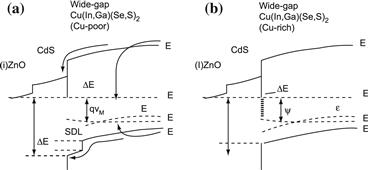
FIGURE 14 Energy band diagram of a ZnO/CdS/(wide-gap) Cu(In,Ga)(Se,S)2 heterojunction. The band diagram (a) that includes the surface defect layer (SDL) of a Cu-poor prepared film shows that the interface recombination barrier ϕ∗bp = ϕbp + ΔEintv is larger than the barrier ϕbp in the device that was prepared Cu-rich (b). The difference is the internal valence band offset ΔEintv between the SDL and the bulk of the absorber. The larger value of ϕ∗bp reduces interface recombination.
Up to now, all arguments for explaining the relatively low performance of wide-gap chalcopyrite alloys deal with the changes in the band diagram. However, recent work focuses on the differences in the electronic quality of the absorber materials. Here, it was found that the concentration of recombination active defects increases when increasing the Ga content in Cu(In,Ga)Se2 above a Ga/(Ga + In) ratio of about 0.3 [32] and the S content in Cu(In,Ga)(Se,S)2 alloys over a S/(Se + S) ratio of 0.3 [34]. Moreover, a recent systematic investigation of the dominant recombination mechanism in large series of Cu(In,Ga)(Se,S)2 based solar cells with different compositions [150] suggests that bulk recombination prevails in all devices that were prepared with a Cu-poor final film composition. Only devices that had a Cu-rich composition (before removing Curich secondary phases) showed signatures of interface recombination. The absence of interface recombination in Cu-poor devices could be a result of the presence of the Cu-poor surface defect layer in these devices. Comparison of Figures 14(a) and (b) illustrates that interface recombination is much more likely to dominate those devices that lack this feature.
5.2 CuGaSe2
CuGaSe2 has a band gap of 1.68 eV and therefore would represent an ideal partner for CuInSe2 in an all-chalcopyrite tandem structure. However, a reasonable efficiency for the top cell of any tandem structure is about 15%, far higher than has been reached by the present polycrystalline CuGaSe2 technology. The record efficiency of CuGaSe2 thin-film solar cells is only 8.3% (9.3% active area) [151] despite of the fact that the electronic properties of CuGaSe2 are not so far from those of CuInSe2. However, in detail, all the differences quantitatively point in a less favourable direction. In general, the net doping density NA in CuGaSe2 appears too high [152]. Together with the charge of deeper defects, the high doping density leads to an electrical field in the space-charge region, which enhances recombination by tunnelling [153]. The high defect density in CuGaSe2 thin films absorbers additionally leads to a low diffusion length and, in consequence, to a dependence of the collected short circuit current density Jsc on the bias voltage V. Because of the decreasing width of the space charge region, Jsc(V) decreases with increasing V affecting significantly the fill factor of the solar cell [130]. Note that, on top of the limitation by the unfavourable bulk properties, interface recombination also plays a certain role in CuGaSe2 [154] because of the unfavourable band diagram shown in Figure 14. Therefore, substantial improvement of the performance requires simultaneous optimisation of bulk and interface properties. Notably, CuGaSe2 is the only Cu-chalcopyrite material where the record efficiency of cells based on bulk crystals (with η = 9.4%, total area) [115] exceeds that of thin-film devices.
5.3 Cu(In,Al)Se2
As can be seen in Figure 2, the bandgap change within the Cu(In,Al)Se2 alloy system is significant even if a small amount of Al is added to CuInSe2 [144]. This fact allows to grow graded structures with only small changes in the lattice constant. Al–Se compounds tend to react with water vapour to form oxides and H2Se. Furthermore, there is a tendency to phase segregations [144]. However, cells with very good performance have been achieved by a co-evaporation process of absorbers in a band gap range between 1.09 and 1.57 eV, corresponding to Al/(In + Al) ratio x between 0.09 and 0.59 [144,156]. The highest confirmed efficiency of a Cu(In,Al)Se2 solar cell is 16.9% [157] (see also Table 3). This device has about the same band-gap energy as the record Cu(In,Ga)Se2 device [1].
5.4 CuInS2 and Cu(In,Ga)S2
The major difference between CuInS2 and Cu(In,Ga)Se2 is that the former cannot be prepared with an overall Cu-poor composition. Cu-poor CuInS2 displays an extremely low conductivity, making it almost unusable as a photovoltaic absorber material [145]. Even at small deviations from stoichiometry on the In-rich side, segregation of the spinel phase is observed [158]. Instead, the material of choice is Cu-rich CuInS2. As in the case of CuInSe2, a Cu-rich preparation route implies the removal of the unavoidable secondary Cu–S binary phase by etching the absorber in KCN solution [147]. Such an etch may involve some damage of the absorber surface as well as the introduction of shunt paths between the front and the back electrode. However, as shown in Table 3, the best CuInS2 device [159] has an efficiency above 11%. This record efficiency for CuInS2 is achieved by a sulphurisation process rather than by co-evaporation.
As we have discussed previously, interface recombination dominates the open circuit voltage Voc of Cu(In,Ga)(Se,S)2 devices that are prepared with a Cu-rich absorber composition (prior to the KCN etch), like the CuInS2 and Cu(In,Ga)S2 devices discussed here. It was found recently, that alloying CuInSe2 with moderate amounts of Ga enhances the open circuit voltage Voc[160]. This increase of Vor can counterbalance the loss of short circuit current density Jsc resulting from the increased band gap. Apparently, addition of Ga to CuInS2 reduces interface recombination by increasing the interfacial barrier ϕbp(cf. Figure 14(b)) [150]. However, for Cu(In,Ga)S2 devices prepared by the sulphurisation route, the benefit of Ga alloying is limited, because, during preparation, most of the Ga added to the precursor ends up confined to the rear part of the absorber layer and, therefore, remains ineffective at the absorber surface [160]. In contrast, when preparing Cu(In,Ga)S2 with co-evaporation, Ga is homogeneously distributed through the depth of the absorber and the Ga content at the film surface is well controlled. Recent work of Kaigawa et al. [148] represents a major progress in wide-gap Cu-chalcopyrites with the preparation of Cu(In,Ga)S2 solar cells with a confirmed efficiency of 12.3% at a band gap energy Eg = 1.53 eV. In the same publication [148] an efficiency of 10.1% is reported for a device with Eg = 1.65 eV. The open circuit voltage Voc of this device is 831 mV, i.e., only slightly lower than Voc of the best CuGaSe2 cell having an efficiency of 8.3%.
5.5 Cu(In,Ga)(Se,S)2
One possible way of overcoming the disadvantages of the ternary wide-gap materials CuInS2 and CuGaSe2 is to use the full pentenary alloy system Cu(In1–xGax)(Se1–ySy)2[146]. Among the materials listed in Table 3, the pentenary system is the only one with an open-circuit voltage larger than 750 mV and an efficiency above 13%, outperforming CuInS2 in both these respects. The advantage of Cu(In,Ga)(Se,S)2 could be due to the mutual compensation of the drawbacks of CuGaSe2 (too high charge density) and that of (Cu-poor) CuInS2 (too low conductivity, if prepared with a Cu-poor film composition).
5.6 Graded-Gap Devices
An interesting property of the Cu(In,Ga,Al)(S.Se)2 alloy system is the possibility of designing graded-gap structures in order to optimise the electronic properties of the final device [161–164]. Such band-gap gradings are achieved during co-evaporation by the control of the elemental sources, but selenisation/sulphurisation processes also lead to beneficial compositional gradings. The art of designing optimum band-gap gradings is to push back charge carriers from critical regions, i.e., regions with high recombination probability within the device. Such critical regions are (i) the interface between the back contact and the absorber layer and (ii) the heterojunction interface between the absorber and the buffer material. Figure 15 shows a band diagram of a graded structure that fulfils the requirements for minimising recombination losses.
1. To keep the back contact region clear from electrons, one can use a Ga/In grading. The increase of the Ga/(Ga + In) ratio causes a movement of the conduction band minimum upward with respect to its position in a non-graded CuInSe2 device. Thus, back surface grading leads to a gradual increase of the conduction-band energy, as illustrated in Figure 15, and therefore drives photogenerated electrons away from the metallic back contact into the direction of the buffer/absorber junction.
2. The minimisation of junction recombination, both at the point of equal capture rates of holes and electrons in the space charge region (recombination path B in Figure 15) as well as at the absorber/buffer interface (path C), requires an increased band gap towards the absorber surface. If one had the choice, one would clearly favour a decrease of the valence-band energy, as shown in Figure 15, over an increase of the conduction band energy. This favours a grading with the help of S/Se alloying, as at least a part of the increasing band-gap energy is accommodated by a decrease of the energy of the valence-band edge that should minimise interface recombination.
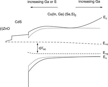
FIGURE 15 Band diagram of a ZnO/CdS/Cu(In,Ga)(Se,S)2 heterojunction with a graded-gap absorber. The minimum band gap energy is in the quasi neutral part of the absorber. An increasing Ga/In ratio towards the back surface and an increasing Ga/In or S/Se-ratio towards the front minimise recombination in critical regions at the back contact (recombination path A’), in the space charge region (path B), and at the heterointerface (path C). The dotted lines correspond to the conduction and valence band edge energies of a non-graded device.
6 Conclusions
The objective of this chapter is the description of the recent achievements on Cu(In,Ga)Se2-based solar cells as well as an account of our present understanding of the physical properties of the materials involved and the electronic behaviour of the devices. Cu(In,Ga)Se2 is in a leading position among polycrystalline thin-film solar cell materials because of the benign, forgiving nature of the bulk materials and interfaces. Nevertheless, we want to guide the attention of the reader also in the direction of the work that has still to be done.
Three of the four cornerstones 1–4 for the recent achievements mentioned in Section 3.2 concern the growth of the films: the optimised deposition conditions and the incorporation of Na and Ga. However, no detailed model is available to describe the growth of Cu(In,Ga)Se2, and especially the impact of Na, which, in our opinion, is the most important of the different ingredients available to tune the electronic properties of the absorber. A clearer understanding of Cu(In,Ga)Se2 growth would allow us to find optimised conditions in the wide parameter space available, and thus to reduce the number of recombination centres and compensating donors and optimise the number of shallow acceptors. The deposition of the buffer layer, or more generally speaking, the formation of the heterojunction, is another critical issue. The surface chemistry taking place during heterojunction formation, and also during post-deposition treatments, is decisive for the final device performance. Both processes greatly affect not only the surface defects (i.e., recombination and charge), and therefore the charge distribution in the device, but also the defects in the bulk of the absorber. Concentrated effort and major progress in these tasks would not only allow us to push the best efficiencies further towards 20%, but would also provide a sound knowledge base for the various attempts at the commercialisation of Cu(In,Ga)Se2 solar cells.
Acknowledgements
The authors thank all our colleagues at the IPE for various discussions and fruitful collaboration. We are especially grateful to J. H. Werner for his continuous support of the Cu(In,Ga)Se2 research at the ipe. We are grateful to M. Turcu for a critical reading of the manuscript. Support of our work during many years by the German Ministry of Research, Technology, and Education (BMBF), by the Ministry of Economics, and by the European Commission is especially acknowledged.
References
1. Contreras M, Egaas B, Ramanathan K, et al. Progress toward 20% efficiency in Cu(In,Ga)Se2 polycrystalline thin-film solar cells. Prog Photovolt Res Appl. 1999;7:311.
2. Kessler J, Bodegard M, Hedström J, Stolt L. New world record Cu(In,Ga)Se2 based mini-module: 16.6%. Glasgow: Proceedings of the 16th European Photovoltaic Solar Energy Conference; 2000; p. 2057.
3. Hahn H, Frank G, Klingler W, Meyer A, Störger G. über einige ternäre Chalkogenide mit Chalkopyritstruktur. Z Anorg u Allg Chemie. 1953;271:153.
4. Wagner S, Shay JL, Migliorato P, Kasper HM. CuInSe2/CdS heterojunction photovoltaic detectors. Appl Phys Lett. 1974;25:434.
5. Mickelsen RA, Chen WS. High photocurrent polycrystalline thin-film CdS/ CuInSe2 solar cell. Appl Phys Lett. 1980;36:371.
6. Mitchell KC, Ermer J, Pier D. Single and tandem junction CuInSe2 cell and module technology. Las Vegas: Proceedings of the 20th IEEE Photovoltaic Specialists Conference; 1988; p. 1384.
7. Wieting RD, CIS. Manufacturing at the megawatt scale. New Orleans: Proceedings of the 29th IEEE Photovoltaic Specialists Conference; 2002; p. 480.
8. Probst V, Stetter W, Riedl W, et al. Rapid CIS- process for high efficiency PV-modules: development towards large area processing. Thin Solid Films. 2001;387:262.
9. Dimmler B, Powalla M, Schock HW. CIS-based thin-film photovoltaic modules: potential and prospects. Prog Photovolt Res Appl. 2002;10:149.
10. Powalla M, Lotter E, Waechter R, Spiering S, Oertel M, Dimmler B. Pilot line production of CIGS modules: first experience in processing and further developments. New Orleans: Proceedings of the 29th IEEE Photovoltaic Specialists Conference; 2002; p. 571.
11. Kushiya K. Improvement of electrical yield in the fabrication of CIGS-based thin- film modules. Thin Solid Films. 2001;387:257.
12. Negami T, Satoh T, Hashimoto Y, Nishiwaki S, Shimakawa S, Hayashi S. Large- area CIGS absorbers prepared by physical vapor deposition. Sol Energy Mater Sol Cells. 2001;67:1.
13. Rau U, Schock HW. Electronic properties of Cu(In,Ga)Se2 heterojunction solar cells-recent achievements, current understanding, and future challenges. Appl Phys A. 1999;69:191.
14. Rau U, Schock HW. Cu(In,Ga)Se2 Solar Cells. In: Archer MD, Hill R, eds. Clean Electricity from Photovoltaics. London: Imperial College Press; 2001; p. 270.
15. Shay JL, Wernick JH. Ternary Chalcopyrite Semiconductors: Growth Electronic Properties, and Applications. Oxford: Pergamon Press; 1975.
16. Kazmerski LL, Wagner S. Cu-ternary chalcopyrite solar cells. In: Coutts TJ, Meakin JD, eds. Current Topics in Photovoltaics. Orlando: Academic Press; 1985; p. 41.
17. Coutts TJ, Kazmerski LL, Wagner S. Ternary Chalcopyrite Semiconductors: Growth, Electronic Properties, and Applications. Amsterdam: Elsevier; 1986.
18. Rockett A, Birkmire RW. CuInSe2 for photovoltaic applications. J Appl Phys. 1991;70:81.
19. Stanbery BJ. Copper indium selenides and related materials for photovoltaic devices. Crit Rev Solid State. 2002;27:73.
20. Haalboom T, Gödecke T, Ernst F, et al. Phase relations and microstructure in bulk materials and thin films of the ternary system Cu-In-Se. Inst Phys Conference Ser. 1997;152E:249.
21. Herberholz R, Rau U, Schock HW, et al. Phase segregation, Cumigration and junction formation in Cu(In,Ga)Se2. Eur Phys J Appl Phys. 1999;6:131.
22. Migliorato P, Shay JL, Kasper HM, Wagner S. Analysis of the electrical and luminescent properties of CuInSe2. J Appl Phys. 1975;46:1777.
23. Noufi R, Axton R, Herrington C, Deb SK. Electronic properties versus composition of thin films of CuInSe2. Appl Phys Lett. 1984;45:668.
24. Zhang SB, Wei SH, Zunger A, Katayama-Yoshida H. Defect physics of the CuInSe2 chalcopyrite semiconductor. Phys Rev B. 1998;57:9642.
25. Neumann H. Vacancy formation in AIBIIIC2VI chalcopyrite semiconductors. Cryst Res Technol. 1983;18:901.
26. Abou-Elfotouh FA, Moutinho H, Bakry A, Coutts TJ, Kazmerski LL. Characterization of the defect levels in copper indium diselenide. Solar Cells. 1991;30:151.
27. Igalson M, Schock HW. The metastable changes of the trap spectra of CuInSe2- based photovoltaic devices. J Appl Phys. 1996;80:5765.
28. Schmitt M, Rau U, Parisi J. Investigation of deep trap levels in CuInSe2 solar cells by temperature dependent admittance measurements. Nice: Proceedings of the 13th European Photovoltaic Solar Energy Conference; 1995; p. 1969.
29. Walter T, Herberholz R, Müller C, Schock HW. Determination of defect distributions from admittance measurements and application to Cu(In,Ga)Se2 based heterojunctions. J Appl Phys. 1996;80:4411.
30. Igalson M, Bacewicz R, Schock HW. ‘Dangling bonds’ in CulnSe2 and related compounds. Nice: Proceedings of the 13th European Photovoltaic Solar Energy Conference; 1995; p. 2076.
31. Herberholz R, Nadenau V, Rühle U, Köble C, Schock HW, Dimmler B. Prospects of wide-gap chalcopyrites for thin film photovoltaic modules. Sol Energy Mater Sol Cells. 1997;49:227.
32. Hanna G, Jasenek A, Rau U, Schock HW. Open circuit voltage limitations in CuIn1–xGaxSe2 thin- film solar cells – dependence on alloy composition. Phys Stat Sol A. 2000;179:R7.
33. Rau U, Schmidt M, Jasenek A, Hanna G, Schock HW. Electrical characterization of Cu(In,Ga)Se2 thin-film solar cells and the role of defects for the device performance. Sol Energy Mater Sol Cells. 2001;67:137.
34. Turcu M, Kötschau IM, Rau U. Composition dependence of defect energies and band alignments in the Cu(In1–xGax)(Se1–ySy)2 alloy system. J Appl Phys. 2002;91:1391.
35. Caldas M, Fazzio A, Zunger A. A universal trend in the binding energies of deep impurities in semiconductors. Appl Phys Lett. 1984;45:67.
36. Langer JM, Heinrich H. Deep-level impurities: a possible guide to prediction of band-edge discontinuities in semiconductor heterojunctions. Phys Rev Lett. 1985;55:1414.
37. Heath JT, Cohen JD, Shafarman WN, Liao DX, Rockett AA. Effect of Ga content on defect states in CuIn1–xGaxSe2 photovoltaic devices. Appl Phys Lett. 2002;80:4540.
38. Turcu M, Rau U. Compositional trends of defect energies, band alignments, and recombination mechanisms in the Cu(In,Ga)(Se, S)2 alloy system. Thin Solid Films. 2003;158:431–432.
39. Herberholz R, Igalson M, Schock HW. Distinction between bulk and interface states in CuInSe2/CdS/ZnO by space charge spectroscopy. J Appl Phys. 1998;83:318.
40. Stolt L, Hedström J, Kessler J, Ruckh M, Velthaus KO, Schock HW. ZnO/CdS/CuInSe2 thin-film solar cells with improved performance. Appl Phys Lett. 1993;62:597.
41. Hedström J, Ohlsen H, Bodegard M, et al. ZnO/CdS/Cu(In,Ga)Se/sub 2/thin film solar cells with improved performance. Lousville: Proceedings of the 23rd IEEE Photovoltaic Specialists Conference; 1993; p. 364.
42. Devaney WE, Chen WS, Steward JM, Mickelson RA. Structure and properties of high efficiency ZnO/CdZnS/CuInGaSe2 solar cells. IEEE Trans Electron Devices ED-37 1990;428.
43. Potter RR, Eberspacher C, Fabick LB. Device analysis of CuInSe2/(Cd, Zn)S solar cells. Las Vegas: Proceedings of the18th IEEE Photovoltaic Specialists Conference; 1985; p. 1659.
44. Birkmire RW, McCandless BE, Shafarman WN, Varrin RD. Approaches for high efficiency CuInSe2 solar cells. Freiburg: Proceedings of the 9th. European Photovoltaic Solar Energy Conference; 1989; p. 134.
45. Contreras MA, Egaas B, Dippo P, et al. On the role of Na and modifications to Cu(In,Ga)Se absorber materials using thin-MF (M5Na, K, Cs) precursor layers. Anaheim: Proceedings of the 26th IEEE Photovoltaic Specialists Conference; 1997; p. 359.
46. Holz J, Karg F, Phillipsborn HV. The effect of substrate impurities on the electronic conductivity in CIGS thin films. Amsterdam: Proceedings of the 12th European Photovoltaic Solar Energy Conference; 1994; p. 1592.
47. Nakada T, Mise T, Kume T, Kunioka A. Superstate type Cu(In,Ga)Se2 thin film solar cells with ZnO buffer layers – a novel approach to 10% efficiency. Vienna: Proceedings of the 2nd. World Conference on Photovoltaic Solar Energy Conversion; 1998; p. 413.
48. Ruckh M, Schmid D, Kaiser M, Schäffler R, Walter T, Schock HW. Influence of substrates on the electrical properties of Cu(In,Ga)Se2 thin films. Hawaii: Proceedings of the First World Conference on Photovoltaic Solar Energy Conversion; 1994; p. 156.
49. Keyes BM, Hasoon F, Dippo P, Balcioglu A, Abouelfotouh F. Influence of Na on the elctro-optical properties of Cu(In,Ga)Se2. Anaheim: Proceedings of the 26th. IEEE Photovoltaic Specialists Conference; 1997; p. 479.
50. Rau U, Schmitt M, Engelhardt P, et al. Impact of Na and S incorporation on the electronic transport mechanisms of Cu(In,Ga)Se2 solar cells. Solid State Commun. 1998;107:59.
51. Braunger D, Hariskos D, Bilger G, Rau U, Schock HW. Influence of sodium on the growth of polycrystalline Cu(In.Ga)Se2 thin films. Thin Solid Films. 2000;361:161.
52. Takei R, Tanino H, Chichibu S, Nakanishi H. Depth profiles of spatially resolved Raman spectra of a CuInSe2-based thin-film solar cell. J Appl Phys. 1996;79:2793.
53. Wada T, Kohara N, Negami T, Nishitani M. Chemical and structural characterization of Cu(In,Ga)Se2/Mo interface in Cu(In,Ga)Se2 solar cells. Jpn J Appl Phys. 1996;35:1253.
54. Klenk R, Walter T, Schock HW, Cahen D. A model for the successful growth of polycrystalline films of CuInSe2 by multisource physical vacuum evaporation. Adv Mat. 1993;5:114.
55. Probst V, Rimmasch J, Stetter W, et al. Improved CIS thin film solar cells through novel impurity control techniques. Nice: Proceedings of the 73th European Photovoltaic Solar Energy Conf.; 1995; p. 2123.
56. Gabor AM, Tuttle JR, Albin DS, Contreras MA, Noufi R, Hermann AM. High-efficiency CuInxGa1–xSe2 solar cells from (Inx, Ga1–x)2Se3 precursors. Appl Phys Lett. 1994;65:198.
57. Binsma JJM, Van der Linden HA. Preparation of thin CuInS2 films via a two- stage process. Thin Solid Films. 1982;97:237.
58. Chu TL, Chu SC, Lin SC, Yue I. Large grain copper indium diselenide films. J Electrochem Soc. 1984;131:2182.
59. Kapur VK, Basol BM, Tseng ES. Lov-cost methods for the production of semiconductor films for CuInSe2/CdS solar cells. Solar Cells. 1987;21:65.
60. Probst V, Karg F, Rimmasch J, et al. Advanced stacked elemental layer progress for Cu(InGa)Se2 thin film photovoltaic devices. Mat Res Soc Symp Proc. 1996;426:165.
61. Niki S, Fons PJ, Yamada A, et al. High quality CuInSe2 epitaxial films – molecular beam epitaxial growth and intrinsic properties. Inst Phys Conference Ser. 1994;152E:221.
62. Gallon PN, Orsal G, Artaud MC, Duchemin S. Studies of CuInSe2 and CuGaSe2 thin films grown by MOCVD from three organometallic sources. Vienna: Proceedings of the 2nd World Conference on Photovoltaic Solar Energy Conversion; 1998; p. 515.
63. Guillemoles J-F, Cowache P, Lusson A, et al. High quality CuInSe2 epitaxial films – molecular beam epitaxial growth and intrinsic properties. J Appl Phys. 1996;79:7293.
64. Abken A, Heinemann F, Kampmann A, et al. Large area electrodeposition of Cu(In,Ga)Se2 precursors for the fabrication of thin film solar cells. Vienna: Proceedings of the 2nd World Conference on Photovoltaic Solar Energy Conversion; 1998; p. 1133.
65. Lincot D, Guillemoles J-F, Cowache P, et al. Solution deposition technologies for thin film solar cells: status and perspectives. Vienna: Proceedings of the 2nd World Conference on Photovoltaic Solar Energy Conversion; 1998; p. 440.
66. Guimard D, Grand PP, Boderau N, et al. Copper indium diselenide solar cells prepared by electrodeposition. New Orleans: Proceedings of the 29th IEEE Photovoltaic Specialists Conference; 2002; p. 692.
67. Eberspacher C, Pauls KL, Fredric CV. Improved processes for forming CuInSe2 films. Vienna: Proceedings of the 2nd World Conf on Photovoltaic Solar Energy Conversion; 1998; p. 303.
68. Eberspacher C, Pauls K, Serra J. Non-vacuum processing of CIGS solar cells. New Orleans: Proceedings of the 29th IEEE Photovoltaic Specialists Conference; 2002; p. 684.
69. Ramanathan K, Bhattacharya RN, Granata J, et al. Advances in the CIS research at NREL. Anaheim: Proceedings of the 26th IEEE Photovoltaic Specialists Conference; 1998; p. 319.
70. Kapur VK, Bansal A, Le P, Asensio OI. Non-vacuum printing process for CIGS Solar cells on rigid and flexible substrates. New Orleans: Proceedings of the 29th IEEE Photovoltaic Specialists Conference; 2002; p. 688.
71. Cahen D, Noufi R. Defect chemical explanation for the effect of air anneal on CdS/CuInSe2 solar cell performance. Appl Phys Lett. 1989;54:558.
72. Rau U, Braunger D, Herberholz R, et al. Oxygenation and air-annealing effects on the electronic properties of Cu(In,Ga)Se2 films and devices. J Appl Phys. 1999;86:497.
73. Kronik L, Rau U, Guillemoles J-F, Braunger D, Schock HW, Cahen D. Interface redox engineering of Cu(In,Ga)Se2-based solar cells: oxygen, sodium, and chemical bath effects. Thin Solid Films. 2000;353:361–362.
74. Scheer R. Surface and interface properties of Cu-chalcopyrite semiconductors and devices. Research Trends in Vacuum Sci Technol. 1997;2:77.
75. Rau U. Role of defects and defect metastabilities for the performance and stability of Cu(In,Ga)Se2 based solar cells. Jpn J Appl Phys. 2000;39(Suppl. 39–1):389.
76. Schmid D, Ruckh M, Grunwald F, Schock HW. Chalcopyritc/defect chalcopyrite heterojunctions on the basis of CuInSe2. J Appl Phys. 1993;73:2902.
77. Morkel M, Weinhardt L, Lohmüller B, et al. Flat conduction-band alignment at the CdS/CuInSe2 thin-film solar-cell heterojunction. Appl Phys Lett. 2001;79:4482.
78. Schmid D, Ruckh M, Schock HW. A comprehensive characterization of the interfaces in Mo/CIS/CdS/ZnO solar cell structures. Sol Energy Mater Sol Cells. 1996;41:281.
79. Contreras MA, Wiesner H, Niles D, et al. Defect chalcopyrite Cu(In1–xGax)3Se5 materials and high Ga-content Cu(In,Ga)Se2- based solar cells. Washington, DC: Proceedings of the 25th IEEE Photovoltaic Specialists,; 1996; p. 809.
80. Niemeegers A, Burgelman M, Herberholz R, Rau U, Hariskos D, Schock HW. Model for electronic transport in Cu(In,Ga)Se2 solar cells. Prog Photovolt Res Appl. 1998;6:407.
81. Bardeen J. Surface states and rectification at a metal semiconductor contact. Phys Rev. 1947;71:717.
82. Klein A, Jaegermann W. Fermi-level-dependent defect formation in Cu-chalcopyrite semiconductors. Appl Phys Lett. 1999;74:2283.
83. Kessler J, Velthaus KO, Ruckh M, et al. Chemical bath deposition of CdS on CuInSe2, etching effects and growth kinetics. New Delhi, India: Proceedings of the 6th. International Photovoltaic Solar Energy Conference; 1992; p. 1005.
84. Friedlmeier TM, Braunger D, Hariskos D, Kaiser M, Wanka HN, Schock HW. Nucleation and growth of the CdS buffer layer on Cu(In,Ga)Se2 thin films. Washington DC: Proceedings of the 25th IEEE Photovoltaic Specialists Conference; 1996; p. 845.
85. Ramanathan K, Wiesner H, Asher S, et al. High efficiency Cu(In,Ga)Se2 thin film solar cells without intermediate buffer layers. Vienna: Proceedings of the 2nd World Conference on Photovoltaic Solar Energy Conversion; 1998; p. 477.
86. Wada T, Hayashi S, Hashimoto Y, Nishiwaki S, Sato T, Nishitina M. High efficiency Cu(In,Ga)Se2 (CIGS) solar cells with improved CIGS surface. Vienna: Proceedings of the 2nd World Conference on Photovoltaic Solar Energy Conversion; 1998; p. 403.
87. Hariskos D, Ruckh M, Rühle U, et al. A novel cadmium free buffer layer for Cu(In,Ga)Se2 based solar cells, Sol. Energy Mater Sol Cells 41/42 1996;345.
88. Kushiya K, Nii T, Sugiyama I, Sato Y, Inamori Y, Takeshita H. Application of Zn-compound buffer layer for polycrystalline CuInSe2-based thin-film solar cells. Jpn J Appl Phys. 1996;35:4383.
89. Kushiya K, Tachiyuki M, Kase T, et al. Improved FF of CIGS thin-film mini-modules with Zn(O,S,OH)x buffer by post- depostion light soaking. Anaheim: Proceedings of the 26th IEEE Photovoltaic Specialists Conference; 1997; p. 327.
90. Nakada T, Furumi K, Kunioka A. High-efficiency cadmium-free Cu(In,Ga)Se-2 thin-film solar cells with chemically deposited ZnS buffer layers. IEEE Trans Electron Devices 1999;(1999):2093 2093ED-46.
91. Nakada T, Mizutani M. 18% efficiency Cd-free Cu(In,Ga)Se2 thin-film solar cells fabricated using chemical bath deposition (CBD)-ZnS buffer layers. Jpn J Appl Phys. 2002;41:L165.
92. Ohtake Y, Kushiya K, Ichikawa M, Yamada A, Konagai M. Polycrystalline Cu (InGa)Se2 thin-film solar cells with ZnSe buffer layers. Jpn J Appl Phys. 1995;34:5949.
93. Ohtake Y, Ichikawa M, Yamada A, Konagai M. Cadmium free buffer layers for polycrystalline Cu(In,Ga)Se2 thin film solar cells. Nice: Proceedings of the 13th European Photovoltaic Solar Energy Conference; 1995; p. 2088.
94. Konagai M, Ohtake Y, Okamoto T. Development of Cu(InGa)Se2 thin film solar cells with Cd-free buffer layers. Mat Res Soc Symp Proc. 1996;426:153.
95. Powalla M, Lotter E, Waechter R, Spiering S, Oertel M, Dimmler B. Pilot line production of CIGS modules: first experience in processing and further developments. New Orleans: Proceedings of the 29th IEEE Photovoltaic Specialists Conference; 2002; p. 571.
96. Hartmann M, Schmidt M, Jasenek A, et al. Flexible and light weight substrates for Cu(In,Ga)Se2 solar cells and modules. Anchorage: Proceedings of the 28th IEEE Photovoltaic Specialists Conference; 2000; p. 638.
97. Tiwari AN, Krejci M, Haug F-J, Zogg H. 12.8% Efficiency Cu(In,Ga)Se2 solar cell on a flexible polymer sheet. Prog Photovolt. 1999;7:393.
98. S. Wiedemann, M.E. Beck, R. Butcher, I. Repins, N. Gomez, B. Joshi, et al., Proceedings of the 29th IEEE Photovoltaic Specialists Conference, New Orleans, 2002, p. 575.
99. Fabick LB, Jehle A, Scott S, Crume B, Jensen G, Armstrong J. A new thin- film space PV module technology. New Orleans: Proceedings of the 29th IEEE Photovoltaic Specialists Conference; 2002; p. 971.
100. Hanket GM, Singh UP, Eser E, Shafarman WN, Birkmire RW. Pilot-scale manufacture of Cu(InGa)Se2 films on a flexible polymer substrate. New Orleans: Proceedings of the 29th IEEE Photovoltaic Specialists Conference; 2002; p. 567.
101. Gay RR. Status and prospects for CIS-based photovoltaics. Sol Energy Mater Sol Cells. 1997;47:19.
102. Karg F, Kohake D, Nierhoff T, Kühne B, Grosser S, Lux-Steiner MC. Performance of grid-coupled PV arrays based on CIS solar modules. Munich: Proceedings of the17th European Photovoltaic Solar Energy Conference; 2002; p. 391.
103. Powalla M, Dimmler B. Process development of high performance CIGS modules for mass production. Thin Solid Films. 2001;387:251.
104. Schmidt M, Braunger D, Schäffler R, Schock HW, Rau U. Influence of damp heat on the electrical properties of Cu(In,Ga)Se2 solar cells. Thin Solid Films. 2001;283:361–362.
105. Igalson M, Wimbor M, Wennerberg J. The change of the electronic properties of CIGS devices induced by the ‘damp heat’ treatment. Thin Solid Films. 2002;320:403–404.
106. Deibel C, Dyakonov V, Parisi J, Palm J, Zweigart S, Karg F. Electrical characterisation of damp-heat trated Cu(In,Ga)(S,Se)2 solar cells. Munich: Proceedings of the 17th European Photovoltaic Solar Energy Conference; 2002; p. 1229.
107. Karg F, Calwer H, Rimmasch J, et al. Development of stable thin film solar modules based on CulnSe2. Inst Phys Conference Ser. 1998;152E:909.
108. Guillemoles J-F, Kronik L, Cahen D, Rau U, Jasenek A, Schock HW. Stability issues of Cu(In,Ga)Se2-based solar cells. J Phys Chem B. 2000;104:4849.
109. Guillemoles JF. The puzzle of Cu(In,Ga)Se2 (CIGS) solar cells stability. Thin Solid Films. 2002;405:403–404.
110. Gay CF, Potter RR, Tanner DP, Anspaugh BE. Radiation effects on thin film solar cells. Kissimmee: Proceedings of the 17th IEEE Photovoltaic Specialists Conference; 1984; p. 151.
111. Mickelsen RA, Chen WS, Stanbery BJ, et al. Development of CuInSe2 cells for space applications. Las Vegas: Proceedings of the 18th IEEE Photovoltaic Specialists Conference; 1985; p. 1069.
112. Jasenek A, Rau U. Defect generation in Cu(In,Ga)Se2 heterojunction solar cells by high-energy electron and proton irradiation. J Appl Phys. 2001;90:650.
113. Walters RJ, Summers GP, Messenger SR, et al. Displacement damage dose analysis of proton irradadiated CIGS solar cells on flexible substrates. Munich: Proceedings of the 17th European Photovoltaic Solar Energy Conference; 2002; p. 2191.
114. Guillemoles J-F, Rau U, Kronik L, Schock HW, Cahen D. Cu(In,Ga)Se2 solar cells: device stability based on chemical flexibility. Adv Mat. 1999;8:111.
115. Jasenek A, Schock HW, Werner JH, Rau U. Defect annealing in Cu(In,Ga)Se2 heterojunction solar cells after high-energy electron irradiation. Appl Phys Lett. 2001;79:2922.
116. Kawakita S, Imaizumi M, Yamaguchi M, et al. Annealing enhancement effect by light illumination on proton irradiated Cu(In,Ga) Se2 thin-film solar cells. Jpn J Appl Phys. 2002;41(2):L797.
117. Jasenek A, Rau U, Weinert K, Schock HW, Werner JH. Illumination- enhanced annealing of electron irradiated Cu(In,Ga)Se2 solar cells. New Orleans: Proceedings of the 29th IEEE Photovoltaic Specialists Conference; 2002; p. 872.
118. Tuttle JR, Szalaj A, Keane J. A 15.2% AM0/1433W/kg thin-film Cu(In,Ga)Se2 solar cell for space applications. Anchorage: Proceedings of the 28th IEEE Photovoltaic Specialists Conference; 2000; p. 1042.
119. Hartmann M, Schmidt M, Jasenek A, et al. Flexible and light weight substrates for Cu(In,Ga)Se2 solar cells and modules. Anchorage: Proceedings of the 28th IEEE Photovoltaic Specialists Conference; 2000; p. 838.
120. Tiwari AN, Krejci M, Haug FJ, Zogg H. 12.8% Efficiency Cu(In,Ga)Se2 solar cell on a flexible polymer sheet. Prog Photov. 1999;7:393.
121. Turcu M, Rau U. Fermi level pinning at CdS/Cu(In,Ga)(Se,S)2 interfaces: effect of chalcopyrite alloy composition. J Phys Chem Solids. 2003;64 p. xxx.
122. Nelson AJ, Schwerdtfeger CR, Wei S-H, et al. Theoretical and experimental studies of the ZnSe/CuInSe2 heterojunction band offset. Appl Phys Lett. 1993;62:2557.
123. Löher T, Jaegermann W, Pettenkofer C. Formation and electronic properties of the CdS/CuInSe2 (011) heterointerface studied by synchrotron-induced photoemission. J Appl Phys. 1995;77:731.
124. Wei S-H, Zunger A. Band offsets at the CdS/CuInSe2 heterojunction. Appl Phys Lett. 1993;63:2549.
125. Ruckh M, Schmid D, Schock HW. Photoemission studies of the ZnO/CdS interface. J Appl Phys. 1994;76:5945.
126. Orgassa K, Nguyen Q, Kötschau IM, Rau U, Schock HW, Werner JH. Optimized reflection of CdS/ZnO window layers in Cu(In,Ga)Se2 thin film solar cells. Munich: Proceedings of the 17th European Photovoltaic Solar Energy Conference; 2002; p. 1039.
127. Engelhardt F, Bornemann L, Köntges M, et al. Cu(In,Ga)Se2 solar cells with a ZnSe buffer layer: interface characterization by quantum efficiency measurements. Prog Photovolt Res Appl. 1999;7:423.
128. Bube RH. Photolectronic Properties of Semiconductors. Cambridge, UK: Cambridge University Press; 1992.
129. Green MA. Solar Cells. Sydney, Australia: University of New South Wales; 1986; p. 96.
130. Shafarman WN, Klenk R, McCandless BE. Device and material characterization of Cu(InGa)Se2 solar cells with increasing band gap. J Appl Phys. 1996;79:7324.
131. Rau U, Schmidt M. Electronic properties of ZnO/CdS/Cu(In,Ga)Se2 solar cells – aspects of heterojunction formation. Thin Solid Films. 2001;387:141.
132. Niemegeers A, Burgelman M, De Vos A. On the CdS/CuInSe2 conduction band discontinuity. Appl Phys Lett. 1995;67:843.
133. Ruberlo MN, Rothwarf A. Time-dependent open-circuit voltage in CuInSe2/ CdS solar cells: Theory and experiment. J Appl Phys. 1987;61:4662.
134. Sasala RA, Sites JR. Time dependent voltage in CuInSe2 and CdTe solar cells. Louisville: Proceedings of the 23rd IEEE Photovoltaic Specialists Conference; 1993; p. 543.
135. Kushia K, Tachiyuki M, Kase T, et al. Fabrication of graded band-gap Cu(InGa)Se2 thin-film mini-modules with a Zn(O,S,OH)x buffer layer. Sol Energy Mater Sol Cells. 1997;49:277.
136. Rau U, Jasenek A, Herberholz R, et al. The inherent stability of Cu(In,Ga)Se2-based solar cells. Vienna: Proceedings of the 2nd World Conference on Photovoltaic Energy Conversion; 1998; p. 428.
137. Zabierowski P, Rau U, Igalson M. Classification of metastabilities in the electrical characteristics of ZnO/CdS/Cu(In,Ga)Se2 solar cells. Thin Solid Films. 2001;387:147.
138. Rau U, Schmitt M, Parisi J, Riedl W, Karg F. Persistent photoconductivity in Cu(In,Ga)Se2 heterojunctions and thin films prepared by sequential deposition. Appl Phys Lett. 1998;73:223.
139. Meyer Th, Schmidt M, Engelhardt F, Parisi J, Rau U. A model for the open circuit voltage relaxation in Cu(In,Ga)Se2 heterojunction solar cells. Eur Phys J App Phys. 1999;8:43.
140. Lang DV, Logan RA. Large-lattice-relaxation model for persistent photoconductivity in compound semiconductors. Phys Rev Lett. 1977;39:635.
141. Delahoy AK, Ruppert A, Contreras M. Charging and discharging of defect states in CIGS/ZnO junctions. Thin Solid Films. 2000;140:161–162.
142. Rau U, Weinert K, Nguyen Q, et al. Mat Res Soc Symp Proc. 2001;668 p. H9.1.1.
143. Siebentritt S. Wide gap chalcopyrites: material properties and solar cells. Thin Solid Films. 2002;1:403–404.
144. Paulson PD, Haimbodi MW, Marsillac S, Birkmire RW, Shafarman WN. CuIn1–xAlxSe2 thin films and solar cells. J Appl Phys. 2002;91:10153.
145. Walter T, Content A, Velthaus KO, Schock HW. Solar-cells based on CuIn(Se,S)2. Sol Energy Mater Sol Cells. 1992;26:357.
146. Friedlmeier TM, Schock HW. Improved voltages and efficiencies in Cu(In,Ga)(S,Se)2 solar cells. Vienna: Proceedings of the 2nd. World Conference on Photovoltaic Solar Energy Conversion; 1998; p. 1117.
147. Scheer R, Walter T, Schock HW, Fearhailey ML, Lewerenz HJ. CuInS2 based thin film solar cell with 10.2% efficiency. Appl Phys Lett. 1993;63:3294.
148. Kaigawa R, Neisser A, Klenk R. M.-Ch Lux-Steiner, Improved performance of thin film solar cells based on Cu(In,Ga)S2. Thin Solid Films. 2002;415:266.
149. Klenk R. Characterisation and modelling of chalcopyritc solar cells. Thin Solid Films. 2001;387:135.
150. Turcu M, Pakma O, Rau U. Interdependence of absorber composition and recombination mechanism in Cu(In,Ga)(Se,S)2 heterojunction solar cells. Appl Phys Lett. 2002;80:2598.
151. Nadenau V, Hariskos D, Schock II W. CuGaSe2 based thin-film solar cells with improved performance. Barcelona: Proceedings of the 14th European Photovoltaic Solar Energy Conference; 1997; p. 1250.
152. Jasenek A, Rau U, Nadenau V, Schock HW. Electronic properties of CuGaSe2- based heterojunction solar cells Part II Defect spectroscopy. J Appl Phys. 2000;vol. 87:594.
153. Nadenau V, Rau U, jasenek A, Schock HW. Electronic properties of CuGaSe2- based heterojunction solar cells Part I Transport analysis. J Appl Phys. 2000;87:584.
154. Reiß J, Malmström J, Werner A, Hengel I, Klenk R, Lux-Steiner MCh. Current Transport in CuInS2 solar cells depending on absorber preparation. Mat Res Soc Symp Proc. 2001;668 p. H9.4.1.
155. Schön JH, Klenk M, Schenker O, Bucher E. Photovoltaic properties of CuGaSe2 homodiodes. Appl Phys Lett. 2000;77:3657.
156. Shafarman WN, Marsillac S, Paulson PD, Haimbodi MW, Birkmire RW. Material and device characterization of thin film Cu(InAl)Se2 solar cells. New Orleans: Proceedings of the 29th IEEE Photovoltaic Specialists Conference; 2002; p. 519.
157. Marsillac S, Paulson PS, Haimbodi MW, Birkmire RW, Shafarman WN. High-efficiency solar cells based on Cu(InAl)Se2 thin films. Appl Phys Lett. 2002;81:1350.
158. Walter T, Schock HW. Structural and electrical investigations of the anion-exchange in polycrystalline CuIn(S, Se)2 thin-films. Jpn J Appl Phys. 1993;32(3):116.
159. Siemer K, Klaer J, Luck I, Bruns J, Klenk R, Bräunig D. Efficient CuInS2 solar cells from a rapid thermal process (RTP). Sol Energy Mater Sol Cells. 2001;67:159.
160. Hengel I, Neisser A, Klenk R, Lux-Steiner MC. Ga/Cds/ZnO – solar cells, Thin Solid Films, 361–362. Current transport in CuInS2 2000;458.
161. Gray JL, Lee YJ. Numerical modeling of graded band gap CIGS solar cells. Hawaii: Proceedings of the First World Conference on Photovoltaic Solar Energy Conversion; 1994; p. 123.
162. Dhingra A, Rothwarf A. Computer simulation and modeling of graded bandgap CuInSe2/CdS based solar cells. IEEE Trans Electron Devices ED-43 1996;613.
163. Gabor AM, Tuttle JR, Bode MH, et al. Band-gap engineering in Cu(In,Ga)Se2 thin films grown from (In,Ga)2Se5 precursors. Sol Energy Mater Sol Cells. 1996;41:247.
164. Dullweber T, Rau U, Contreras M, Noufi R, Schock HW. Photogeneration and carrier recombination in graded gap Cu(In Ga)Se2 solar cells. IEEE Trans Electron Dev ED-47 2000;2249.