
Chapter IA-2
Semiconductor Materials and Modelling
Chapter Outline
2. Semiconductor Band Structure
3. Carrier Statistics in Semiconductors
6. Carrier Generation by Optical Absorption
7.1. Bulk Recombination Processes
7.3. Minority-Carrier Lifetime
1 Introduction
Solar cell modelling is fundamental to a detailed understanding of the device operation, and a comprehensive model requires a detailed knowledge of the material parameters. A brief overview of the semiconductor properties relevant to solar cell operation is given in this chapter, including the semiconductor band structure and carrier statistics, transport and optical properties, recombination processes, material aspects of radiation damage to solar cells in space and effects observed under heavy doping, with special attention given to the properties of hydrogenated amorphous silicon. The principal semiconductor parameters encountered in photovoltaic applications are summarised in Tables 1 and 2. The refractive indices of materials used for antireflection coating can be found in Table 3.
TABLE 1 Properties of the Principal Semiconductors with Photovoltaic Applications (all at 300 K). Bandgap: d = Direct; i = Indirect. Crystal Structure: Dia = Diamond, Zb = Zinc Blende, Ch = Chalcopyrite. The Refractive Index is given at the Wavelength 590 nm (2.1 eV) Unless Otherwise Stated. Principal Sources of Data: c-Si [20]; GaAs [3]; InP [4,41]; a-Si [5] and Section 10; CdTe [6]; CIS [7]; AlxGa1-xAs [9]. Details of the Absorption Coefficient and Refractive Index, Including the Wavelength Dependence, can be Found in References [27] and [28]. X is the Electron Affinity and TEC Stands for Thermal Expansion Coefficient
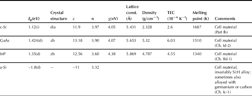
TABLE 2 The Energy gap Eg, Refractive Index n and the Electron Affinity X of Transparent Conducting Semiconductors Used as Window Layers in Thin-Film Solar Cells

TABLE 3 The Refractive Index at 590 nm (2.1 eV) of the Common Materials used for Antireflection Coating. The full-Wavelength Dependence of Most of these Substances can be Found in References [27] and [28]
| Material | n |
| MgF2 | 1.38 |
| SiO2 | 1.46 |
| Al2O3 | 1.76 |
| Si3N4 | 2.05 |
| Ta2O5 | 2.2 |
| ZnS | 2.36 |
| SiOx | 1.8–1.9 |
| TiO2 | 2.62 |
Numerous computer programs that use the material parameters to model solar cell operation have been developed over the years, and several are now available commercially:
• PC1D, developed by P.A. Basore and colleagues at the University of New South Wales, Australia, is the standard one-dimensional simulator used by the PV community.
• ATLAS, a device simulation software by SILVACO International, uses physical models in two and three dimensions. It includes the Luminous tool, which computes ray tracing and response of solar cells. It allows the use of monochromatic or multispectral sources of light.
• MEDICI by Technology Modelling Associates models the two-dimensional distribution of potential and carrier concentration in a semiconductor device. It also includes an optical device advanced application module in which photogeneration can be computed for multispectral sources.
Some programs are available free of charge. These include, for example, SimWindows which can be downloaded from www-ocs.colorado.edu/SimWindows/simwin.html.
A discussion of the main principles of the numerical techniques can be found in specialised texts that deal with the modelling of solar cells (see, for example, the review [1]) or with the modelling of semiconductor devices in general [2].
2 Semiconductor Band Structure
The energy gap (or band gap) Eg and its structure as a function of the wave vector are key characteristics of the semiconductor material and of fundamental importance to the operation of the solar cell (see Figure 1). The principal features of interest are the temperature variation of the band-gap energy Eg and the magnitude of wave vector associated with low-energy transitions.

FIGURE 1 The energy gaps in Si (a), and GaAs and InP (b) as functions of the wave vector k. The inset shows the Brillouin zone of the corresponding face-centred cubic crystal lattice.
The variation of the band gap with temperature can be described by an expression originally suggested by Varshni [10]
![]() (1)
(1)
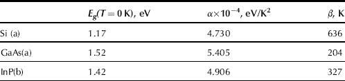
where T is the absolute temperature and the parameters α and β are given in Table 4.
TABLE 4 The Parameters Eg0, α, and β in Equation (1). Sources of Data: (a) Thurmond [11]; (b) Varshni [10]
The current produced by solar cells is generated by optical transitions across the band gap. Two types of such transitions can be distinguished: (1) direct transitions where the momentum of the resulting electron–hole pair is very close to zero, and (2) indirect transitions where the resulting electron–hole pair has a finite momentum. The latter transitions require the assistance of a phonon (quantum of lattice vibration). Thus, there are two types of semiconductors:
• direct gap semiconductors where the top of the valence band and the bottom of the conduction band lie at the Γ point of the first Brillouin zone (i.e., at zero wave vector k = 0); and
• indirect gap semiconductors where the minima of the conduction band (in general, more than one) lie at a another point of the first Brillouin zone, with a different value of the wave vector k.
The optical absorption in indirect-gap semiconductors is considerably weaker than in direct-gap semiconductors, as shown in Figure 2 on the example of silicon and gallium arsenide.
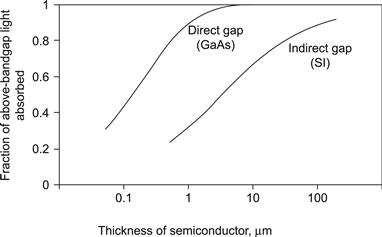
FIGURE 2 A comparison of the difference in strength of the optical absorption in direct and indirect semiconductors, illustrated on the examples of silicon and gallium arsenide.
3 Carrier Statistics in Semiconductors
In thermal equilibrium, the temperature and the electrochemical potential (the Fermi level, denoted by EF) are constant throughout the device. The product of the electron concentration n and the hole concentration p is then independent of doping and obeys the mass action law
![]() (2)
(2)
where kB is the Boltzmann constant, ni is the electron (or the hole) concentration in the intrinsic semiconductor, and the effective densities of states Nc and Nv are given by
![]() (3)
(3)
Here, h is the Planck constant and me and mh are the electron and hole density-of-states effective masses (see Table 5). In Equation (3), the effective mass me includes a factor that allows for several equivalent minima of the conduction band in indirect-gap semiconductors (see Figure 1).
TABLE 5 The Densities of States in the Conduction and Valence Band (Nc and Nv, Respectively), the Intrinsic Carrier Concentration n1 and the Density-of-States Effective Masses me and mh (all at 300 K) in Si, GaAs and InP. m0 Denotes the Free-Electron Mass.

Data from References [20,35]; Intrinsic Carrier Concentration in Si from Reference [12]
Equation (2) does not hold for a solar cell in operation. Current flow as well as electron transitions between different bands or other quantum states are induced by differences and gradients of the electrochemical potentials, and temperature gradients may also exist. It is then usual to assign a quasi-Fermi level to each band that describes the appropriate type of carriers. Thus, electrons in the conduction band will be described by the quasi-Fermi level EFn, and holes by EFp. It is convenient to define also the appropriate potentials Φn and Φp by
![]() (4)
(4)
The use of quasi-Fermi levels to describe solar cell operation was already mentioned in Section 4.1 of Chapter Ia-1. The formalism leads to expressions for electron and hole concentrations, which are summarised in Table 6.
TABLE 6 Carrier Concentration in Degenerate and Nondegenerate Semiconductors. F1/2 Denotes the Integral 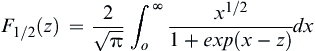

4 The Transport Equations
The electron and the hole current densities Jn and Jp are governed transport by the transport equations
![]() (5)
(5)
where n and p are the electron and the hole; the concentrations μn and μp are the electron and the hole mobilities; Dn and Dp are the electron and the hole diffusion constants; and ε is the electric field. The first term in each equation is due to drift in the electric field ε, and the second term corresponds to carrier diffusion. With the help of the quasi-Fermi levels, the equations in (5) can be written as
![]() (6)
(6)
The equations in (6) are valid for a semiconductor with a homogeneous composition and when position-dependent dopant concentration is included. A generalisation to semiconductors with position-dependent band gaps can be found, for example, in [13].
In a region where space charge exists (for example, in the junction), the Poisson equation is needed to link the electrostatic potential ψ with the charge density ρ:
![]() (7)
(7)
with
![]() (8)
(8)
![]() (9)
(9)
where ε is the static dielectric constant of the semiconductor (see Table 1).
In nondegenerate semiconductors, the diffusion constants are related to mobilities by the Einstein relations
![]() (10)
(10)
The generalisation of the Einstein relations to degenerate semiconductors is discussed, for example, in [14].
The conservation of electrons and holes is expressed by the continuity equations
 (11)
(11)
where G and U are the generation and recombination rates, which may be different for electrons and holes if there are transitions into or from localised states.
5 Carrier Mobility
In weak fields, the drift mobilities in Equations (5) represent the ratio between the mean carrier velocity and the electric field. The mobilities—which are generally different for majority and minority carriers—depend on the concentration of charged impurities and on the temperature. For silicon, these empirical dependencies are generally expressed in the Caughey–Thomas form [15]:
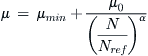 (12)
(12)
The values of the various constants for majority and minority carriers are given in Tables 7 and 8. A full model that includes the effects of lattice scattering, impurity scattering, carrier–carrier scattering, and impurity clustering effects at high concentration is described in [16], where the reader can find further details.
TABLE 7 The Values of Parameters in Equation (12) for Majority-Carrier Mobility in Silicon
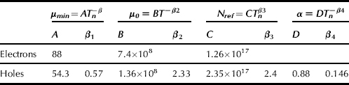
(from Reference [17]; Tn = T/300)
TABLE 8 The Values of Parameters in Equation (12) for Minority-Carrier Mobility in Silicon
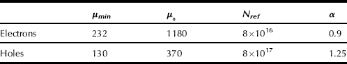
TABLE 9 Parameters in Equation (12) that were used to Fit the Room-Temperature Electron and Hole Mobilities in InP
In strong fields, the mobility of carriers accelerated in an electric field parallel to the current flow is reduced since the carrier velocity saturates. The field dependence of the mean velocity v (only quoted reliably for majority carriers) is given by
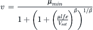 (13)
(13)
where μlf is the appropriate low field value of the mobility (Equation (12)), the parameter β = 2 for electrons and β = 1 for holes, and vsat is the saturation velocity, identical for electrons and holes [20]:
![]() (14)
(14)
In gallium arsenide, the empirical fitting of the mobility data is of a more complex nature, and the reader is referred to the reference [21] for more information regarding the majority-carrier mobility. The temperature and dopant concentration dependences of the minority-carrier mobility are shown in Figures 3 and 4.

FIGURE 3 The temperature dependence of the minority-carrier mobility in GaAs. Full symbols: electron mobility in p-type GaAs (NA = 4×1018 cm−3); data from [22]. Empty symbols: hole mobility in n-type GaAs (ND = 1.8×1018 cm−3) [23]. The dashed lines show fits to the data with expressions
![]()
where T is the temperature in K.

FIGURE 4 The dopant concentration dependence of the room-temperature minority-carrier mobility in GaAs. Full symbols: electron mobility in p-type GaAs; data from [21]. Empty symbols: hole mobility in n-type GaAs [23]. The dashed lines show fits to the data with the expressions
![]()
where ND and NA are the donor and acceptor concentrations in cm−3.
The electric field dependence of carrier mobility in GaAs is different from silicon as the velocity has an ‘overshoot’ that is normally modelled by the following equation [24]:
![]() (15)
(15)
where μlf is the appropriate low-field mobility, ε0 = 4×10³ V/cm, β equals 4 for electrons and 1 for holes, and vsat is given by [25]
![]() (16)
(16)
where T is the temperature in K.
The majority-carrier mobility in indium phosphide reported in reference [26] is shown in Figure 5.
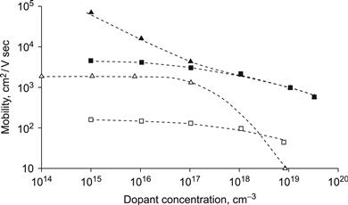
FIGURE 5 The majority-carrier mobilities in InP [26]. Full symbols correspond to electron mobility, empty symbols to hole mobility. Room temperature (300 K) data are shown by squares; data at 77 K by triangles. The room-temperature data were fitted with a Caughey–Thomas-type expression with parameters shown in Table 9.
6 Carrier Generation by Optical Absorption
6.1 Band-to-Band Transitions
The principal means of carrier generation in solar cells is the absorption of light. For a planar slab (Figure 6), a photon that enters the semiconductor generates g(x) δx electron–hole pairs in a thin layer at depth x → x+δx. The generation function g(x) is given by
![]() (17)
(17)
where α(λ) is the absorption coefficient, shown in Figure 7 for a number of semiconductors with photovoltaic applications. The generation rate G per unit volume that appears in Equation (11) is related to the generation function g in Equation (17) by G = g/A, where A is the illuminated area of the sample.

FIGURE 6 The geometry used to discuss the light absorption in semiconductors.
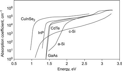
FIGURE 7 The absorption coefficients of the principal semiconductors used in the manufacture of solar cells. Full details of these and other semiconductors can be found in references [27] and [28]. Further details of silicon absorption are given in the text.
A useful formula for the absorption coefficient of silicon is provided by the expression of Rajkanan et al. [29]:
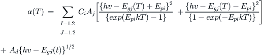 (18)
(18)
where hv is the photon energy, Eg1(0) = 1.1557 eV, Eg2(0) = 2.5 eV, and Egd(0) = 3.2 eV are the two lowest indirect and the lowest direct band gap, respectively (used here as parameters to obtain a fit to the spectrum); Ep1 = 1.827×10⁻² eV and Ep2 = 5.773×10⁻² eV are the Debye frequencies of the transverse optical and transverse acoustic phonons, respectively; and C1 = 5.5, C2 = 4.0, A1 = 3.231×102 cm−1 eV−2, A2 = 7.237×103 cm−1 eV−2, and A1 = 1.052×106 cm−1 eV−2. The temperature variation of the band gaps is described by Equation (1) where the original Varshni coefficients α = 7.021×10⁻⁴, eV/K2 and β = 1108 K are used for all three band gaps Eg1, Eg2, and Egd.
6.2 Free-Carrier Absorption
In regions with high-carrier concentration (due to doping or strong illumination, for example), photon absorption can also occur by electron transitions with initial and final states inside the same band. This free-carrier absorption does not generate electron–hole pairs and competes with the band-to-band transitions that produce the photogenerated current, which were discussed above. Free-carrier absorption might be significant in the case of photon energies near the band gap and should not be included in the absorption coefficient α in front of the exponential in Equation (17). Figure 8 illustrates the different phenomena that occur near the band edge for high doping concentrations.
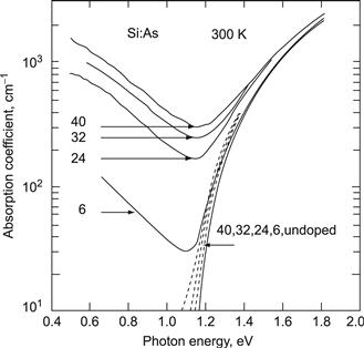
FIGURE 8 The effects observed near the absorption edge at high doping concentrations, illustrated here on the example of n-type silicon.
(from reference [30] as adapted by M.A. Green, Silicon Solar Cells—see Bibliography)
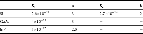
Based on experimental data of [30] and [31], the PC1D model, for example, uses the following expression for the absorption coefficient due to free-carrier absorption:
![]() (19)
(19)
where λ is in nanometres and the empirically determined constants K1, K2, α, and b are given in Table 10.
TABLE 10 The Constants for the Free-Carrier Absorption Coefficient in Equation (19)
7 Recombination
Recombination processes can be classified in a number of ways. Most texts distinguish between bulk and surface recombination, and between band-to-band recombination as opposed to transitions with the participation of defect levels within the band gap. Recombination processes can also be classified according to the medium that absorbs the energy of the recombining electron–hole pair: radiative recombination (associated with photon emission) or the two principal nonradiative mechanisms by Auger and multiphonon transitions, where the recombination energy is absorbed by a free charge carrier or by lattice vibrations, respectively. An opposite process to Auger recombination (in which an electron–hole pair is generated rather than consumed) is called impact ionisation.
The following sections give a brief summary of the main recombination mechanisms with relevance to solar cell operation, which are summarised schematically in Figure 9.

FIGURE 9 A schematic diagram of the principal recombination processes in semiconductors and the notation for the rate constant adopted in this book. The direction of arrows indicates electron transitions.
7.1 Bulk Recombination Processes
A detailed discussion of the variety of the bulk recombination mechanisms can be found in [32]. Here, we confine ourselves to a brief overview of the radiative, Auger and defect-assisted recombination processes that are most frequently encountered in practical operation of solar cells. These processes are depicted schematically in Figure 9, which also shows the notation used to describe the relevant parameters.
The rate of band-to-band radiative recombination can be written in the form
![]() (20)
(20)
where the coefficient B is sometimes written as R/ni2. Radiative transitions between a free electron and a localised state within the band gap may also be important in certain situations—for example, in novel concepts such as the impurity photovoltaic effect. The values of B for silicon, gallium arsenide, and indium phosphide can be found in Table 11. In other situations, the radiative recombination coefficient B can be determined from optical absorption using the detailed balance argument due to van Roosbroeck and Shockley [33].
TABLE 11 The Coefficients B of the Radiative Recombination Rate (Equation (20)) and Cn0 and Cp0 of the Auger Recombination Rate (Equation (21))

Sources of data: (a) [34]; (b) [32]; (c) [35]; (d) [26]
The rate of band-to-band Auger recombination can be written as
![]() (21)
(21)
where the first bracket gives the two, usually most important, Auger terms. Table 11 gives values of the coefficients Cpo and Cno for Si, GaAs and InP.
The recombination rate via defects of concentration Nt with a level at energy Et within the band gap is described by the Shockley–Read–Hall formula [36,37]:
![]() (22)
(22)
where
![]() (23)
(23)
and τn, τp are parameters, proportional to the defect concentration Nt, that are characteristic for the particular defect and energy level. At low injection, τn and τp assume the meaning of minority-carrier lifetimes. With an appropriate dependence on the doping concentration and temperature, τn and τp are also used extensively in material and device modelling (see reference [20], Section 1.5.3 and Section 7.3 for a fuller discussion).
7.2 Surface Recombination
Surface recombination velocity is an important parameter that affects the dark saturation current and the quantum efficiency of solar cells. Similarly to dislocations and planar defects such as grain boundaries, surfaces (and interfaces in general) introduce band of electronic states in the band gap that can be ascribed to broken (or strained) bonds and impurities. A complete characterisation of surface recombination must also take into account the surface charge, which may give rise to band bending. To achieve optimal operation, surface recombination is reduced by a passivating or window layer that prevents minority carriers from reaching the surface. Passivation of silicon surface by an oxide layer or the deposition of a thin ‘window’ layer of GaAlAs on GaAs solar cells are just two examples of such practice.
For an oxidised silicon surface, surface recombination velocity is strongly dependent on the surface roughness, contamination, and ambient gases used during oxidation and the annealing conditions. Under identical process parameters, however, one can identify trends in the dependence of the surface recombination velocity on the surface doping concentration. Cuevas et al. [38] proposed the following analytical relationship between surface recombination velocity and doping concentration:
 (24)
(24)
Equation (24) models several experimental results such as those reported in [39].
In gallium arsenide, the surface recombination velocity is very high (of the order of 106 cm/s). The deposition of a thin layer of GaAlAs, however, reduces the recombination velocity at the interface to 10–103 cm/s (see reference [40], p. 41). Coutts and Yamaguchi [41] quote the values of 103−2×104 cm/s and 1.5×105 cm/s for the surface recombination velocity in n- and p-type InP, respectively.
7.3 Minority-Carrier Lifetime
Under low injection—a regime of particular importance for solar cell operation—the majority-carrier concentration can be assumed excitation independent, and the effect of recombination can be discussed in terms of minority-carrier lifetime. In p-type material, for example, the recombination rate can be written as
![]() (25)
(25)
where τn is the minority-carrier (electron) lifetime. An analogous equation can be written for the hole lifetime τp in n-type material. The inverse of the lifetime—the rate constant—is a sum of the different contributions to the lifetime:
![]() (26)
(26)
where τ stands for τn or τp, as appropriate. This additive nature of the recombination rate constant is also useful when discussing the radiation damage (see Section 8).
The effect of lifetime on transport properties by carrier diffusion can be discussed in terms of the diffusion length defined by
![]() (27)
(27)
where D is the diffusion constant for the minority carriers in question. If, however, drift in electric field ε is the dominant transport mechanism, it is appropriate to define thre drift length as
![]() (28)
(28)
for electrons and holes as minority carriers. This parameter plays an important role in the analysis of p–i–n junction solar cells (see Section 4.3 in Chapter Ia-1).
The wealth of available data for crystalline silicon have made it possible to arrive at a consensus as to the magnitude as well as the temperature and doping-concentration dependence of the contributions (26) to minority-carrier lifetime [42]. The contribution to lifetime due to defects, when combined with recombination in intrinsic material, has been empirically observed to follow the equations
 (29)
(29)
where the first term in the brackets applies for recombination in intrinsic semiconductor. Similarly, the contribution to Equation (26) by Auger recombination can be described by the expressions
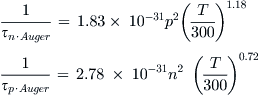 (30)
(30)
Although the concept of minority-carrier lifetime is most commonly applied to bulk recombination, a similar notion can be relevant for surface processes. For example, the effective lifetime observed of minority carriers with uniform concentration in a wafer can be written as
![]() (31)
(31)
where S is the value of the recombination velocity, W is the wafer thickness, and A is the area of the sample.
8 Radiation Damage
Solar cells that operate on board a satellite in an orbit that passes through the Van Allen belts are subjected to fluxes of energetic electrons and protons trapped in the magnetic field of Earth and by fluxes of particles associated with high solar activity [43,44] (see Chapter IId-2). When slowed down in matter, most of the energy of the incident proton or electron is dissipated by interaction with the electron cloud. A relatively small fraction of this energy is dissipated in collisions with the nuclei, resulting in the formation of a lattice defect when energy in excess of a minimum threshold value is transferred to the nucleus [45,46]. A proton with energy in excess of this threshold causes the most damage (typically, of the order of 10–100 atomic displacements) near the end of its range in the crystal. At high energy, on the other hand, a proton creates simple point defects, and the displacement rate decreases with increasing proton energy. In contrast, the displacement rate by electrons increases rapidly with energy and approaches a constant value at higher energies. Electron damage can usually be assumed to be uniform throughout the crystal.
Some defects that are thus created act as recombination centres and reduce the minority-carrier lifetime τ. Thus, it is the lifetime τ (or, equivalently, the diffusion length L) that is the principal quantity of concern when the cell is subjected to the particle radiation in space. Under low injection, the reduction of the diffusion length L is described by the Messenger–Spratt equation (see, for example, [47], p. 151):
![]() (32)
(32)
where L0 is the diffusion length in the unirradiated cell, ϕ is the particle fluence (integrated flux), and KL is a (dimensionless) diffusion-length damage constant characteristic for the material and the type of irradiation.
The damage constant KL generally depends on the type of dopant, and even in single-junction cells, a different damage constant should therefore be introduced for each region of the cell. Moreover, care should be exercised when dealing with low-energy protons (with energy of the order of 0.1–1 MeV), which are stopped near the surface and may create nonuniform damage near the junction. Figures 10 and 11 show the doping concentration and energy dependence of the damage constant KL for electrons and protons in p-type silicon. Details of the damage constants for other materials can be found in references [43], [44], [48], and [49].
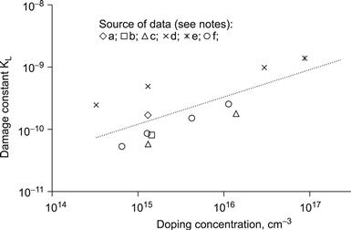
FIGURE 10 The radiation damage constant KL for 1 MeV electrons in p-type silicon as a function of the dopant concentration. Source of data: (a) [50]: (b) [51]; (c) [52]; (d) [53]; (e) [54]; (f) [55]. The dashed line shows a fit to the data with the formula KL = 3.43×10⁻¹⁷NA0.436, where NA is the acceptor concentration in cm−3.

FIGURE 11 The energy dependence of the damage constant KL in 1 Ω-cm p-type silicon by electron (full symbols, [55]) and protons (empty symbols, [56]).
Damage constants are usually quoted for 1 MeV electrons and converted to other energies and particles (such as protons) by using the concept of damage equivalent. Conversion tables are available in the Solar Radiation Handbooks that will suit most circumstances. Radiation damage equivalence works well when applied to uniform damage throughout the cell, but care should be exercised in the case of nonuniform damage—for example, for low-frequency protons.
The reduction of the diffusion length describes usually the most significant part of the damage, but changes in other parameters on irradiation also sometimes need to be considered. The dark diode current I0 may increase as a result of compensation by the radiation-induced defects. This, however, occurs usually at a fluence orders of magnitude higher than that which degrades τ or L. Other source of degradation may be defects created in the depletion region, at the interfaces between different regions of the cell, or at the external surfaces.
9 Heavy Doping Effects
At high doping densities, the picture of independent electrons interacting with isolated impurities becomes insufficient to describe the electron properties of semiconductors. As doping concentration increases, an impurity band is formed from the separate Coulomb wave functions located at individual doping impurities. This band gradually merges with the parent band and eventually gives rise to a tail of localised states. Electron–electron interaction becomes important, and the exchange and correlation energy terms have to be taken into account for a satisfactory description of the optical parameters and semiconductor device operation. An early overview of this multifaceted physical problem can be found in [57].
In practical situations, this complex phenomenon is usually described in terms of band-gap narrowing, with a possible correction to effective masses and band anisotropy. Different manifestations of this effect are normally found by optical measurements (including absorption and low-temperature luminescence) and from data that pertain to device operation. Parameters that have been inferred from the latter are usually referred to as apparent band-gap narrowing, denoted by ΔEg. For n-type material, for example,
![]() (33)
(33)
where p0 is the minority-carrier (hole) concentration and ND is the dopant (donor) concentration.
The experimental data obtained by various methods have been reviewed in [58]. where the reader can find references to much of the earlier work. Jain et al. [59,60] obtain a fit for band-gap narrowing in various materials using a relatively simple and physically transparent expression that, however, is less easy to apply to device modelling. Values for silicon that are now frequently used in semiconductor devices modelling are based on the work of Klaassen et al. [61]. After reviewing the existing experimental data and correcting for the new mobility models and a new value for the intrinsic concentration, Klaassen et al. show that the apparent band-gap narrowing of n- and p-type silicon can be accurately modelled by a single expression:
 (34)
(34)
where Ndop is the dopant concentration.
For gallium arsenide, Lundstrom et al. [62] recommend the following formula based on fitting empirical data:
![]()
where EF is the Fermi energy, the function F1/2 is defined in the caption to Table 5, and
![]()
10 Properties of Hydrogenated Amorphous Silicon1
In hydrogenated amorphous silicon (a-Si:H), the effective band gap between the conduction and valence band edges is around 1.8 eV, but a thermal shrinking of the band gap with temperature has been reported [63]:
![]() (35)
(35)
For statistical calculations, the corresponding effective densities of states can be approximated by Nc ≈ Nv ≈ 4×1019 cm−3. In contrast to crystalline silicon, the conduction and valence bands show evidence of exponential tails of localised states within the band gap [64]:
 (36)
(36)
In addition, there is a Gaussian distribution of dangling bond states (states corresponding to nonsaturated silicon bonds) around midgap (Figure 12):
![]() (37)
(37)
In device-quality intrinsic a-Si:H films, the density of dangling bonds NDB ranges from 1015 to 1016 cm−3.
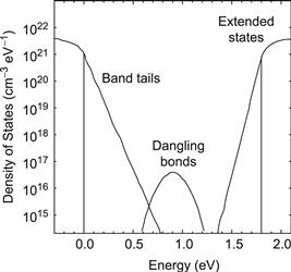
FIGURE 12 Typical density of states in a-Si:H. The states in the band tails behave as carrier traps whereas dangling bonds are recombination centres. Only those carriers in the extended states contribute to the electron transport [65].
The carrier mobility in the localised states (band tails and dangling bonds) is negligible. The accepted values for extended states in the valence and conduction band are μp = 0.5 cm2/V-s and μn = 10 cm2/V-s, respectively. As in other semiconductors, the electron transport is given by the drift-diffusion equations (5) where the Einstein relations (10) apply.
The optical absorption coefficient shows three different zones (Figure 13):
• Band-to-band transitions (Tauc plot) for photon energies in excess of the band gap (>1.8 eV).
• Transitions involving tail states (Urbach’s front) for photon energies in the range 1.5–1.8 eV.
• Transitions involving dangling bonds for photon energies below 1.5 eV.

FIGURE 13 Typical optical absorption coefficient in a-Si:H. Three different regions can be observed corresponding to band-to-band absorption, transitions involving tail states, and defect-associated absorption [65].
Once the optical absorption coefficient is known, the carrier generation can be easily calculated according to Equation (17), but it is important to note that only photons with energies in excess of the band gap yield useful electron–hole pairs for photovoltaic conversion.
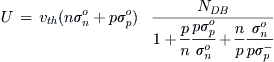
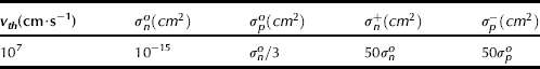
Finally, the dominant recombination mechanism in intrinsic a-Si:H is given by the modified Shockley–Read–Hall equation, as applied to the amphoteric distribution of dangling bonds:
 (38)
(38)
where the parameters are given in Table 12 [66].
TABLE 12 Recombination Parameters in Amorphous Silicon
Acknowledgements
We are grateful to J. Puigdollers and C. Voz for providing graphs of the absorption coefficient and the density of states in amorphous silicon.
References
1. Schwartz RJ. The application of numerical techniques to the analysis and design of solar cells. In: Coutts TJ, Meakin JD, eds. 1990; Current Topics in Photovoltaics. vol. 4 p. 25.
2. Selberherr S. Analysis and Simulation of Semiconductor Devices. Vienna, New York: Springer; 1984;.
3. Brozel MR, Stillman GE, eds. Properties of Gallium Arsenide. London: IEE/ INSPEC, Institution of Electrical Engineers; 1996;.
4. Pearsall TP, ed. Properties, Processing and Applications of Indium Phosphide. London: INSPEC/IEE; 2000;.
5. Shur M. Physics of Semiconductor Devices. Englewood Cliffs, NJ: Prentice Hall; 1990;.
6. Chu TL. Cadmium telluride solar cells. In: Coutts TJ, Meakin JD, eds. 1988; Current Topics in Photovoltaics. vol. 3 p. 235.
7. Kazmerski LL, Wagner S. Cu-ternary chalcopyrite solar cells. In: Coutts TJ, Meakin JD, eds. 1985; Current Topics in Photovoltaics. vol. 1 p.41.
8. Handbook of Physics and Chemistry of Solids. eightysecond ed. Boca Raton: CRC Press; 2001;.
9. Adachi S. GaAs, AlAs and AlxGa1-xAs: material parameters for use in research and device applications. J Appl Phys. 1985;58 R 1.
10. Varshni YP. Temperature dependence of the energy gap in semiconductors. Physica. 1967;34:149.
11. Thurmond CD. The standard thermodynamic functions for the formation of electrons and holes in Ge, Si, GaAs and GaP. J Electrochem Soc. 1975;122:1133.
12. Sproul AB, Green MA. Intrinsic carrier concentration and minority-carrier mobility of silicon from 77-K to 300-K. J Appl Phys. 1993;73:1214–1225.
13. Marshak AH, van Vliet KM. Electrical currents in solids with position dependent band structure. Solid-State Electron. 1978;21:417.
14. Smith RR. Semiconductors. In: second ed. Cambridge: Cambridge University Press; 1978.
15. Caughey DM, Thomas RE. Carrier mobilities in silicon empirically related to doping and field. Proc IEEE. 1967;55:2192.
16. Klaassen DBM. A unified mobility model for device simulation-l Model equations and concentration dependence. Solid-State Electron. 1992;35:953–959.
17. Arora ND, Hauser TR, Roulston DJ. Electron and hole mobilities in silicon as a function of concentration and temperature, IEEE Trans. Electron Dev. 1982;ED-29:292.
18. Swirhun SE, Kwark Y-H, Swanson RM. Measurement of electron lifetime, electron mobility and band-dap narrowing in heavily doped p-type silicon. IEDM’86 1986;24–27.
19. del Alamo J, Swirhun S, Swanson RM. Simultaneous measurement of hole lifetime, hole mobility and band-gap narrowing in heavily doped n-type silicon. IEDM’85 1985;290–293.
20. Sze SM. Physics of Semiconductor Devices. second ed. New York: John Wiley & Sons; 1981.
21. Lancefield D. Electron mobility in GaAs: overview. In: Brozel MR, Stillman GE, eds. Properties of Gallium Arsenide. third ed. London: IEE/INSPEC, Institution of Electrical Engineers; 1996;41.
22. Harmon ES, Lovejoy ML, Lundstrom MS, Melloch MR. Minority electron mobility in doped GaAs. In: Brozel MR, Stillman GE, eds. Properties of Gallium Arsenide. third ed. London: IEE/INSPEC, Institution of Electrical Engineers; 1996;81.
23. Lovejoy ML, Melloch MR, Lundstrom MS. Minority hole mobility in GaAs. In: Brozel MR, Stillman GE, eds. Properties of Gallium Arsenide. third ed. London: IEE/INSPEC, Institution of Electrical Engineers; 1996;123.
24. Barnes JJ, Lomax RJ, Haddad GI. Finite element simulation of GaAs MESFET’s with lateral doping profiles and submicron gates, IEEE Trans. Electron Dev. 1976;ED-23:1042.
25. Littlejohn MA, Hauser JR, Glisson TH. Velocity-field characteristics of GaAs with Γc6–L6c–Xc6 ordering. J Appl Phys. 1977;48:4587.
26. Ahrenkiel RK. Minority carrier lifetime in InP. In: Pearsall TP, ed. Properties, Processing and Applications of Indium Phosphide. London: INSPEC/IEE; 2000.
27. Palik ED, ed. Handbook of Optical Constants of Solids. Orlando: Academic Press Handbook Series; 1985.
28. Palik ED, ed. Handbook of Optical Constants of Solids II. San Diego: Academic Press; 1991.
29. Rajkanan K, Singh R, Shewchun J. Absorption coefficient of silicon for solar cell calculations. Solid-State Electron. 1979;22:793.
30. Schmid PE. Optical absorption in heavily doped silicon. Phys Rev. 1981;B23:5531.
31. Fan HY. In: Willardson RK, Beer AC, eds. Academic Press 1967;409. Semiconductors and Semimetals. vol. 3.
32. Landsberg PT. Recombination in Semiconductors. Cambridge University Press 1991.
33. van Roosbroeck W, Shockley W. Photon-radiative recombination of electrons and holes in germanium. Phys Rev. 1954;94:1558.
34. M.H. Pilkuhn, Light emitting diodes, in: T.S. Moss (Ed.), vol. 4, Handbook of Semiconductors, North Holland, p. 539.
35. Handbook Series on Semiconductor Parameters. vols. 1 and 2. Levinstein M, Rumyantsev S, Shur M, eds. London: World Scientific; 1996; 1999 (See also http://www.ioffe.rssi.ru/SVA/NSM/Semicond/; 1996; ).
36. Shockley W, Read WT. Statistics of the recombination of holes and electrons. Phys Rev. 1952;87:835.
37. Hall RN. Electron hole recombination in germanium. Phys Rev. 1952;87:387.
38. Cuevas A, Giroult-Matlakowski G, Basore PA, du Bois C, King R. Extraction of the surface recombination velocity of passivated phosphorus doped emitters. Hawaii: Proc. 1st World Conference on Photovoltaic Energy Conversion; 1994; pp. 1446– 1449.
39. King RR, Sinton RA, Swanson RM. Studies of diffused emitters: saturation current, surface recombination velocity and quantum efficiency. IEEE Trans Electron Dev ED-37 1990;365.
40. Andreev VM, Grilikhes VA, Rumyantsev VD. Photovoltaic Conversion of Concentrated Sunlight. Chichester: Wiley; 1997.
41. Coutts TJ, Yamaguchi M. Indium phosphide based solar cells: a critical review of their fabrication, performance and operation. In: Coutts TJ, Meakin JD, eds. 1988;79. Current Topics in Photovoltaics. vol. 3.
42. Klaassen DBM. A unified mobility model for device simulation—II Temperature dependence of carrier mobility and lifetime. Solid-State Electron. 1992;35:961.
43. Tada HY, Carter JR, Anspaugh BE, Downing RG. Solar-Cell Radiation Handbook. Pasadena, CA: Jet Propulsion Laboratory, California Institute of Technology; 1982; JPL Publication 82–69.
44. Anspaugh BE. GaAs Solar Cell Radiation Handbook. Pasadena, CA: Jet Propulsion Laboratory, California Institute of Technology; 1996; JPL Publication 96–9.
45. Kinchin GH, Pease RS. The displacement of atoms in solids by radiation, Rep. Prog Phys. 1955;18:1.
46. Seitz F, Koehler JS. Displacement of atoms during irradiation. Solid State Phy. 1956;2:307.
47. Hovel HJ. Semiconductor solar cells. In: Willardson RK, Beer AC, eds. New York: Academic Press; 1975; Semiconductors and Semimetals. vol. 11.
48. Markvart T. Radiation damage in solar cells. J Mater Sci.: Mater Electron. 1990;1:1.
49. Yamaguchi M, Ando K. Mechanism for radiation resistance of InP solar cells. J Appl Phys. 1988;63:5555.
50. Smits FM. IEEE Trans Nucl Sci NS-10 1963;88.
51. Meulenberg A, Treble FC. Damage in silicon solar cells from 2 to 155MeV protons. Palo Alto: Proc. 10th IEEE Photovoltaic Specialists Conf.; 1973; p. 359.
52. Rosenzweig W. Diffusion length measurement by means of ionizing radiation. Bell Syst Tech J. 1962;41:1573–1588.
53. Wilsey ND. Proc 9th IEEE Photovoltaic Specialists Conf., Silver Springs 1972;338.
54. Minahan JA, Green MJ. Proc 18th IEEE Photovoltaic Specialists Conf. 1985;350.
55. Downing RG, Carter Jr JR, Denney JM. The energy dependence of electron damage in silicon. Proc 4th IEEE Photovoltaic Specialists Conf. 1964;1 A-5–1.
56. Rosenzweig W, Smits FM, Brown WL. Energy dependence of proton irradiation damage in silicon. J Appl Phys. 1964;35:2707.
57. Keyes RW. The energy gap of impure silicon, Comm. Solid State Phys. 1977;7(6):149.
58. Wagner J, delAlamo JA. Band-gap narrowing in heavily doped silicon: a comparison of optical and electrical data. J Appl Phys. 1988;63:425.
59. Jain SC, Roulston DJ. A simple expression for bandgap narrowing in heavily doped Si Ge, GaAs and GexSi1−x strained layers. Solid-State Electron. 1991;34:453.
60. Jain SC, McGregor JM, Roulston DJ, Balk P. Modified simple expression for bandgap narrowing in n-type GaAs. Solid-State Electron. 1992;35:639.
61. Klaassen DBM, Slotboom JW, de Graaf HC. Unified apparent bandgap narrowing in n and p-type silicon. Solid-State Electron. 1992;35:125.
62. Lundstrom MS, Harmon ES, Melloch MR. Effective bandgap narrowing in doped GaAs. In: Brozel MR, Stillman GE, eds. Properties of Gallium Arsenide. third ed London: IEE/INSPEC, Institution of Electrical Engineers; 1996;186.
63. Tsang C, Street RA. Phys Rev. 1979;B19 3027.
64. Fritzsche H, ed. Amorphous Silicon and Related Materials. University of Chicago 1989.
65. J. Puigdollers, C. Voz, personal communication.
66. Street RA. Hydrogenated Amorphous Silicon. Cambridge University Press 1991.
1A rigorous description of the band structure and charge carrier transport in amorphous silicon is a complex matter well beyond the scope of this handbook. This section gives a simplified picture in terms of effective parameters that has been used in success in semiconductor device modelling.