
Chapter IIA-1
Characterization and Diagnosis of Silicon Wafers, Ingots, and Solar Cells
Chapter Outline
2. Factors Affecting Carrier Recombination
3. Measurement of the Minority-Carrier Lifetime
3.2. Interpretation of Effective Lifetime Measurements
3.2.1. Surface Recombination Velocity
3.2.2. Emitter Saturation Current Density
3.3. Lifetime Measurements in Silicon Ingots
3.4. Lifetime Instabilities and Measurement Artifacts
3.4.1. Lifetime Changes in Boron-Doped CZ Silicon and Iron-Contaminated Silicon
3.4.2. High Apparent Lifetime at Low Excess Carrier Densities
4. Relationship Between Device Voltage and Carrier Lifetime
5. Applications to Process Monitoring and Control of Silicon Solar Cells
5.2. Process Monitoring via Lifetime Measurements
5.2.1. Measurements of Carrier Lifetime in an Ingot or Brick
5.2.2. Lifetime Measurements on Bare Wafers
5.2.3. Effective Lifetime After Emitter Formation
5.3. Device-Level Characterization
5.3.1. Standard Diode Analysis of Suns–Voc Curves
5.3.2. Monitoring Contact Formation
1 Introduction
Monitoring the fabrication process of a solar cell entails measurements of mechanical, optical, and electronic properties of the silicon wafers and the different layers and coatings formed on them. This chapter focuses on electronic characterization, with emphasis on measurements of the effective minority-carrier lifetime and their interpretation to extract relevant information about the silicon material, the emitter regions, and the surface passivation. The chapter also includes a brief description of techniques based on photo and electroluminescence that can provide high-resolution images of ingots, wafers, and devices. A direct measurement of the open-circuit voltage under variable illumination gives the Suns–Voc characteristics, which provide most of the parameters needed to model solar cells at the device level, including diode saturation current, ideality factor, shunt resistance, and the upper bound on fill factor. The application of these techniques to process monitoring and control is described for the case of silicon solar cells, illustrating the correlation between the effective lifetime measured at various stages of fabrication and device performance. Final I-V curve testing at one-sun illumination and 25°C temperature is routinely integrated in solar cell production lines following standard methods that are described elsewhere in this book.
2 Factors Affecting Carrier Recombination
Once created within a semiconductor, photogenerated electrons and holes last, on average, a finite time called the lifetime. When carriers are continuously generated, as in a solar cell, the value of the lifetime determines the stable population of electrons and holes. This population should desirably be as high as possible because it determines the voltage produced by the device. A second, equally important aspect of the lifetime is that it is directly related to the diffusion length, which is the average distance that carriers can travel from the point of generation to the point of collection (the p–n junction). The relationship between L and τ is L = √(Dnτn), with a value for the diffusion coefficient of Dn = 27 cm2/s, for electrons (minority carriers) in 1-Ωcm p-type silicon. The diffusion length should be greater than the wafer thickness or the longest generation depth to ensure a high short-circuit current. Since the lifetime determines both the voltage and the current of the device, its characterization is of the utmost importance.
The lifetime should not be assumed to be a constant single value. It can change considerably, depending on the process history of the sample (including possible contamination and thermal degradation) and measurement conditions (injection level and temperature), and it can degrade or recover when the sample is exposed to light or annealed at certain temperatures. The measured, apparent lifetime can also be affected by nonrecombination mechanisms such as carrier trapping. Figure 1 shows, as an example, the lifetime measured over a broad range of carrier-density injection levels for two float-zone (FZ) silicon wafers, one of which was purposely contaminated with iron. The behavior of the lifetime can be understood in most cases with the assistance of the theoretical models that describe the most important physical mechanisms. It should be kept in mind that the measured lifetime, τeff, may include several of them simultaneously.

FIGURE 1 Measured effective-carrier lifetime τeff as a function of the excess carrier concentration Δn for a 1-Ωcm boron-doped FZ silicon wafer contaminated with iron before and after light soaking, which dissociates iron–boron pairs. An uncontaminated control wafer is also shown. Both had the surfaces passivated with PECVD SiN.
In practical silicon wafers, the most important recombination losses occur through crystallographic defects and impurities that create energy levels within the band gap. The effect of such recombination centers can be described by the Shockley–Read–Hall model, which predicts that the injection-level dependence of the lifetime, τSRH, is a function of the dopant density, NA; recombination center density. NSRH; defect energy level, ET; and capture cross-sections:
![]() (1)
(1)
In this expression, which applies to p-Si, Δn = Δp is the excess carrier density (assuming negligible trapping), and τn0 and τp0 are the fundamental electron and hole lifetimes, which are related to the recombination center density, the thermal velocity vth = 1.1×10⁷ cms−1, and the capture cross-sections via τn0 = 1/(vthσnNSRH) and τp0 = 1/(vthσpNSRH). The magnitudes n1 and p1 are given by
![]() (2)
(2)
The values for the effective densities of states at the conduction and valence band edges are NC = 2.86×10¹⁹ and NV = 3.10×1019 cm−3. For recombination centers located near the middle of the energy gap, Equation (1) predicts an increased lifetime between very low and very high injection level from τno to τno + τpo. Nevertheless, every recombination centre is characterized by a distinctive set of parameters ET, τn0, and τp0. This leads to different injection and temperature dependences of the lifetime and can be used to identify the characteristic signature of each centre. The diversity of possible lifetime curves and the determination of ET, τn0, and τp0 based on the injection level or temperature dependence of the lifetime are reviewed in [1] Figure 1, which is part of an injection-level study for the case of iron–boron pairs in silicon [2], shows a good fit of Equation (1) to the experimental data. The light-soaked results in which the iron–boron pairs are dissociated show a widely varying lifetime in the low-injection range of interest for solar cells.
The upper limit to lifetime that may be measured for an otherwise perfect silicon sample is determined by two intrinsic mechanisms: Coulomb-enhanced Auger and radiative band-to-band recombination, with Auger being the most restrictive. The following empirical expressions for the intrinsic lifetime, incorporating both of these mechanisms, for p-type and n-type silicon are widely used [3]:
![]() (3)
(3)
![]() (4)
(4)
It should be emphasized that these two expressions are based on fitting experimental measurements of well surface-passivated long-lifetime samples, and they should not be taken as absolute physical limits. With improved surface passivation, slightly higher lifetimes have already been measured, although an alternative empirical expression has not yet been proposed. For perspective, Equation (3) is plotted in Figure 1 for a 1-Ωcm boron-doped wafer. Even though the intrinsic lifetime “limit” is quite high, it has a strong dependence on carrier density at high injection and should therefore be taken into account when using injection-level dependence techniques to discriminate between different recombination mechanisms, as described in the following sections.
3 Measurement of the Minority-Carrier Lifetime
As mentioned above, the minority-carrier lifetime that can be measured experimentally in a given sample is an effective parameter that encompasses several different recombination and transport mechanisms, including surface recombination. Accordingly, it is labeled here τeff. For a detailed characterization of silicon wafers and devices, it is essential to discriminate between the various physical mechanisms and factors that affect the effective lifetime. Several well-established methods to perform such analysis are described in the following sections.
3.1 Lifetime-Testing Methods
There are three basic approaches to measure the carrier lifetime, depending on the way that an excess of carriers is generated and varied in the semiconductor. In the transient decay method, the photogeneration is terminated abruptly and the rate at which carriers disappear, dn/dt, is measured, together with the excess electron concentration itself, Δn (note that every photon generates one electron–hole pair, so that Δn = Δp). If no current is flowing from the device, then the rate of carrier density change is equal to the recombination rate:
![]() (5)
(5)
Equation (5) implies an exponential decay of the carrier density with time, which means that 37% of electrons are still present after one lifetime, decreasing to 5% after three lifetimes. This method, classically known as photoconductance decay (PCD) [4], is quite robust, because it is based on the measurement of the relative change of Δn with time. It is, nevertheless, advisable to measure the absolute value of Δn at which the lifetime has been determined, since the lifetime is, in general, strongly dependent on the carrier injection level.
In the steady-state method [5], a constant generation rate of known value is maintained, and the lifetime is determined from the balance between generation and recombination:
![]() (6)
(6)
This simple expression assumes a uniform generation rate across the thickness of the sample and also a uniform excess carrier density, Δn. Nevertheless, in cases where they may be nonuniform, Equation (6) is still applicable, with Δn representing an average value. If the illumination varies slowly, quasi–steady-state conditions prevail within the semiconductor, leading, for example, to the quasi–steady-state photoconductance method (QSSPC) [6].
 (7)
(7)
Equation (7) is applicable to the three experimental situations and is frequently referred to as the generalized method [7]. An absolute measurement of the excess carrier density, Δn, is required to determine the lifetime in the steady state and QSSPC methods. In addition, the photogeneration rate needs to be determined accurately as well. The latter is measured using a photodetector (for example, a calibrated solar cell). The detector gives the total photon flux incident on the surface of the wafer. For the standard AM1.5G solar spectrum commonly referred to as one-sun intensity (100 mW cm−2) the number of photons per second and cm2 with energy above the energy band gap of silicon (photon energy above 1.12 eV) is Nph = 2.7×1017 cm−2. This photon flux gives, multiplied by the electronic charge, an upper limit of the current density for a silicon solar cell, 43.5 mA cm−2. Silicon wafers absorb only a fraction of these photons, depending on the reflectivity of the front and back surfaces, possible faceting of those surfaces, and the thickness of the wafer. The value of the absorption fraction for a polished, bare silicon wafer of thickness 250 μm is fabs ≈ 0.6. If the wafer has an optimized antireflection coating, such as a 70-nm-thick silicon nitride or titanium oxide layer, fabs ≈ 0.9, while a textured wafer with antireflection coating can approach fabs ≈ 1. The uncertainties associated with the determination of fabs can be kept very small by using tables or graphs that can be calculated using optical models. The generation rate per unit volume GL can then be evaluated from the incident photon flux and the wafer thickness:
![]() (8)
(8)
For all three testing methods, the excess electron concentration, Δn, needs to be measured. There are several techniques to do this based on different properties of semiconductor materials. The simplest and most common of them is to measure the conductance of the wafer and the way it changes with illumination and time. The excess photoconductance for a wafer of thickness W is given by
![]() (9)
(9)
Typical mobility values for 1-Ωcm silicon in low injection are μn = 1100 cm2 V−1 s−1 for electrons and μp = 400 cm2 V−1 s−1 for holes. The electron and hole mobilities are functions of the dopant density and injection level, as has been amply documented in the literature [8].
A straightforward way to measure the photoconductance is to apply electrical contacts to the silicon (typically an ingot or a wafer), forcing an electric current through it and measuring the resulting voltage drop [9]. This can also be done in a contactless fashion by using an inductively coupled radio-frequency circuit that produces a voltage proportional to the conductivity of the wafer. This method, implemented in commonly used QSSPC testing instruments, has the added advantage that the relationship between conductance and voltage is practically linear over a broad range [10]. Typical microwave-detected PCD systems, μ-PCD, are based on directing a microwave beam to the silicon wafer and measuring the reflected microwave power, which is proportional to the conductance of the wafer [11,12], although only under carefully optimized configurations [13]. Schroder [14] gives a comprehensive description of these methods, their theoretical background and practical implementation.
The excess carrier density can also be directly determined by probing the sample with infrared light and measuring the amount of free-carrier absorption [15,16] or by using an infrared camera to visualize the free-carrier IR absorption or emission for the entire wafer, which is the basis for the infrared lifetime mapping [17] or carrier density imaging [18] techniques.
Excess carriers may also be detected via photons emitted during radiative band-to-band recombination. Although the fraction of recombination events occurring via this mechanism is small, sensitive detectors have allowed accurate techniques based on Electroluminescence (EL) and Photoluminescence (PL) to be developed. EL is based on the application of a forward bias to generate carriers within a finished device. It can be used, for example, to image spatially resolved diffusion lengths of minority carriers [19,20]. PL uses illumination to generate the excess carriers, and so does not require the presence of a metallized p–n junction. It can therefore be applied at the wafer level, even without surface passivation. The PL emission rate is proportional to Δn(Ndop + Δn) but also depends sensitively on the optical properties of the test sample [21]. This makes absolute calibration of the technique somewhat complicated for the steady-state case, which is the mode commonly used for imaging applications. Nevertheless, by direct comparison to an excess carrier density measured on the same sample via another technique, such as the QSSPC, it is possible to obtain a calibrated, rapid, high-resolution image of the effective lifetime across a sample [22]. The high spatial resolution, on the order of 100 μm, makes the technique ideal for process monitoring, allowing cracks, scratches and contaminated regions to be identified.
Additional methods, also described in [14], such as the surface photovoltage (SPV) and the short-circuit current response, measure the minority-carrier diffusion length. Both rely on the formation of a surface space charge region to collect minority carriers. The SPV approach achieves this by chemically treating the surface so that a surface charge is created that forms the space charge region. A transparent contact is used to measure the voltage associated to the collection of carriers by the space charge region. The latter is usually in the mV range to maintain linearity and simplify the analysis. The formation of a liquid electrolyte–semiconductor junction that allows the extraction of the short-circuit current is also possible and constitutes the basis for the Elymat technique [14]. When a junction exists in the device, as in a finished solar cell, it may be preferable to measure the spectral response of the short-circuit current, an analysis of which can give information on the bulk diffusion length, surface recombination velocity and optical light trapping [23].
Depending on the specific details of their practical implementation, in particular the magnitude of the excitation used, lifetime-testing methods can be broken down into two categories, large-signal and small-signal methods. In R&D laboratories, μ-PCD often uses short pulses to create a relatively small number of carriers in the semiconductor in order to operate in the low-injection range of the detector where the signal can be proportional to the excess carrier density [13]. The resulting small signal is then separated from the background conductance provided by the doping or a bias light. It should be kept in mind that the direct result of measurements using a bias light are, in general, different from the true recombination lifetime. Converting the small-signal lifetime into the actual lifetime requires measuring the former as a function of injection level, followed by integration [24,25]. Industrial μ-PCD systems often use a large-signal approach, which include excitation carrier densities comparable to or higher than the doping levels [26]. Using such testing conditions, the reported values can differ substantially from the actual lifetime since they are a convolution of the lifetime with the sensor nonlinearity [13] as well as the nonlinearity of the photoconductance Equation (9). The microwave-detected photoconductance (MDP) technique is similar to the μ-PCD methodologies, except that it allows for a long excitation pulse [27].
A comparison of contactless lifetime measurement techniques is shown in Table 1. All of them can be used to measure the excess carrier density, and therefore Equations (5) and (9) form a common basis for their analysis, which enables comparisons and complementarities between them.
TABLE 1 Contactless Sensing Methods Commonly Used for Measuring the Excess Carrier Concentration and Lifetime in Silicon
| Technique | Excess carrier-density sensing method | Pros/Cons |
| RF-QSSPC | Eddy-current sensing of photoconductance. Conversion to Δn using known mobility function |
Simple calibration, valid over very wide range of carrier density. Requires mobility and photogeneration model or measurement. Low spatial resolution. Trapping and depletion region modulation effects at low carrier density. |
| RF-transient PCD | Same as QSSPC. | Same as QSSPC, except that no calibration of photogeneration is required. |
| ILM/CDI | IR free-carrier absorption or emission. Calibration using samples of known majority-carrier density. |
High-resolution imaging capability. Surface texture complicates interpretation. Subject to trapping and DRM effects. |
| μ-PCD/MDP | Microwave sensing of photoconductance. Carrier density set by bias light, long-excitation pulse into SS conditions, or by injecting known number of photons in a very short pulse. |
High-resolution mapping capability. Nonlinear detection of photoconductance in some injection-level or dopant ranges; skin depth comparable to sample thickness in some cases. DRM and trapping effects at low carrier density. |
| Photoluminescence | Radiative band to band emission. Models for coefficient of radiative emission and reabsorption, or calibration via another method such as QSSPC. |
Used in both nonimaging and high-resolution imaging applications. Signal depends on doping, photon reabsorption, surface texture, detector EQE, and wafer thickness. Unaffected by trapping and DRM effects, it can be applied at very low carrier densities. |
3.2 Interpretation of Effective Lifetime Measurements
3.2.1 Surface Recombination Velocity
The effective lifetime, τeff, is the net result of summing up all the recombination losses that occur within the different regions that constitute a given silicon sample. The ability to separate out the different recombination mechanisms and identify where the major losses occur within the wafer or the solar cell device is an essential part of the characterization and diagnosis process. For example, if the sample is a silicon wafer, the surfaces usually have a significant impact on the measured effective lifetime. In the special case that the excess carrier density is uniform, the effective lifetime can be expressed mathematically in a relatively simple form:
![]() (10)
(10)
where W is the thickness of the wafer and the surface recombination velocities, Sfront and Sback represent in simplified form the recombination occurring at the front and back sides of the wafer. Equation (10) indicates that measurements of the effective lifetime can be used to study surface recombination. The latter is due to Shockley–Read–Hall processes and can vary with the carrier injection level, in much the same way as the bulk lifetime [28], making a separation between surface and bulk recombination difficult. Nevertheless, it is always possible to determine an upper bound for S by assuming τbulk = ∞ (or τbulk = τintrinsic) in Equation (10), which works quite well when wafers with a very high bulk lifetime are used. Conversely, a lower bound for the bulk carrier lifetime can be obtained by making S = 0 in Equation (10), which applies especially to wafers with a high-quality passivation on both sides. A complete separation between surface and bulk recombination, is possible by using several (at least two) wafers with different thicknesses and identical bulk and surface properties [14].
The assumption of a uniform carrier density that underlies Equation (10) can be self-consistently checked for transient methods if the measured effective lifetime is much greater than the transit time of carriers across the wafer.
![]() (11)
(11)
When this condition is met, the transient method becomes independent of the details of the light pulse excitation, such as wavelength and duration. By waiting a transit time before analyzing the data, excess carriers can spread and distribute themselves evenly across the wafer, even if they were nonuniformly generated. The diffusion coefficient for low-injection conditions in p-type material, is Dn, but in the general case it becomes injection dependent [29]:
![]() (12)
(12)
The transit time depends quadratically on the wafer thickness. In addition, it also depends on the type and doping density of the wafer through the diffusion coefficient, which can vary in the range of 9–30 cm2/s for typical n- and p-type silicon wafers. For symmetric wafers with the same surface recombination velocity on both sides, the requirement of uniform carrier density can be relaxed for the QSSPC method [30].
Equation (10) is a simplified expression, and would predict a zero effective lifetime when the surface recombination velocity is very high. In reality there is a limit on how low the effective lifetime can be because electrons and holes have to diffuse toward the surfaces in order to recombine, which is a relatively slow mechanism. For homogeneous steady-state photogeneration, such as that produced by infrared light, or for a transient decay measurement, the minimum effective lifetime is, respectively, given by the following expressions:
![]() (13)
(13)
![]() (14)
(14)
For a typical p-type 300-μm-thick wafer and an electron diffusion coefficient Dn = 27 cm2 s−1, the lifetime that can be expected for a transient decay measurement is τeff=3.4 μs. The steady-state surface-limited lifetime is a function of the bulk lifetime τbulk and diffusion length Ln, and also of the wavelength spectrum of the light source. In the limit Ln ![]() W, Equation (13) simplifies to τeff(QSSPC) = W2/(12Dn).
W, Equation (13) simplifies to τeff(QSSPC) = W2/(12Dn).
The dependence of the measured effective lifetime on the surface recombination velocity is shown in Figure 2 for the example of a 300-μm-thick, 1-Ωcm p-type wafer and four different values of the bulk lifetime. The graph indicates the lifetime that would be measured for this wafer with either 400-nm or 1000-nm light using a steady-state photoconductance method. The curves were calculated for minority-carrier densities in low injection conditions using the PC1D computer software package [31]. Transient methods, using a short pulse with evaluated with Equation (1), will determine the lifetime approximately as shown by the 1000 nm curves, except that in the limit of high surface recombination the difference between the measured effective lifetime and the actual bulk lifetime is reduced by 22%, as follows from Equation (14). Several main features can be identified on this plot.
1. The measured effective lifetime is equivalent to the actual bulk lifetime if the surfaces are well passivated, independent of the wavelength of illumination (lower part of Figure 2). The demands on surface passivation can, nevertheless, be relaxed when determining relatively low bulk lifetimes. For example, for 0.1 μs bulk lifetime surface recombination velocities up to 1000 cm/s can be tolerated. On the other hand, to accurately determine high bulk lifetimes requires very good passivation. For example, the surface recombination velocity should be less than 10 cm/s to determine τbulk > 100 μs.
2. If the surface recombination velocity is greater than 105 cm/s, typical of unpassivated silicon wafers, infrared light (for example, 1000 nm) measurements are more indicative of the bulk lifetime. The sensitivity to τbulk is excellent if the latter is lower than 2 μs and a one-to-one correspondence can be made between the IR measured effective lifetime and the actual bulk lifetime. The sensitivity is still reasonable to resolve bulk lifetimes up to 10 μs, but is poor for higher lifetimes. Importantly, however, a pass-fail test for τbulk up to 10 μs can be established for bare, unpassivated wafers by using infrared light. For example, a measured lifetime of 2 μs indicates an actual bulk lifetime greater than 10 μs. A more detailed study is given in [32].
3. When the surface recombination velocity is greater than 1000 cm/s (upper portion of Figure 2), the effective lifetime is significantly different for blue and IR light, and this allows the bulk lifetime and the surface recombination velocity to be uniquely determined by measuring with both wavelengths [33]. For example, from Figure 2, a wafer that measures 0.65 μs with 1000-nm light and 0.05 μs with 400-nm light has a bulk lifetime of 1 μs and a surface recombination velocity of 1×105 cm/s. This method exploits the fact that the photogeneration from blue light is very sensitive to the front surface recombination velocity, while the IR light penetrates deep into the bulk of the wafer. Note that the higher lifetime range (above 10 μs) cannot be discriminated even using this method, because the relatively high SRV above 1000 cm/s completely masks bulk recombination.
FIGURE 2 Effective lifetime for a 300-μm, 1-Ωcm p-type wafer as a function of the surface recombination velocity. The curves, modelled with PC1D for steady-state conditions, correspond to wafers with 0.1-, 1-, 10-, and 100-μs bulk lifetimes. Two sets of curves are shown, for 400-nm and 1000-nm monochromatic illumination, respectively.
3.2.2 Emitter Saturation Current Density
Highly doped or emitter regions in silicon solar cells can be formed by thermal diffusion, laser doping or ion implantation. They are commonly characterized by a saturation current density parameter, Joe, that encompasses recombination within the bulk of the thin heavily doped region as well as the recombination at the emitter doped surface. If both sides of a wafer are diffused and the excess carrier density is uniform, then the effective lifetime can be expressed as
![]() (15)
(15)
In this expression, NA is the dopant density of the wafer, assumed here to be p-type, while Joe(front) and Joe(back) are the saturation current densities that characterize the front and back emitter regions, respectively. At 25°C, qni2 = 12 C cm−6.
It is straightforward to consider the case when one of the surfaces is diffused (hence characterized by an emitter saturation current) and the other is not (hence characterized by a surface recombination velocity) by combining Equations (10) and (15). In fact, both concepts are equivalent in low injection, Seff ≈ JoNA/qni2. The scale on the right of Figure 2 shows the emitter-saturation current densities that correspond to the surface recombination velocities on the left axis, for a 1-Ωcm wafer. Equations (10) and (15) assume an approximately uniform carrier density across the wafer. The region of applicability of this assumption is visually displayed in Figure 2 as the region where the 400-nm curves and the 1000-nm curves overlap.
Usually, symmetrically diffused wafers are used to determine the saturation current density. It is possible to determine an upper bound for Joe by performing a measurement in low injection and assuming τbulk = ∞ (or, even better, τbulk = τintrinsic) in Equation (15), if the wafer doping and thickness are known. It is worth noting that a given Joe places a bound on the carrier lifetime that may be observed experimentally, especially for relatively high dopant densities [34,35].
The fact that the emitter recombination term has a different dependence on the carrier injection level than the bulk (SRH and intrinsic) recombination terms allows determination of the Joe by examining the injection level dependence of the lifetime, particularly in the high-injection regime. This method, widely used in conjunction with high resistivity, low NA wafers, was first proposed by Kane and Swanson [36].
Figure 3 shows a family of curves for different values of emitter saturation current density and a bulk doping of 1.5×1016 cm−3 (1 Ωcm). The data are plotted as inverse measured lifetime, following the form of Equation (15). This equation indicates that for measurements performed at minority-carrier densities above the dopant density, the emitter saturation current density will be given by the slope of the line for each curve in Figure 3. The variations in lifetime due to the SRH recombination in the 1/τbulk term occur primarily at carrier densities less than the doping level, so that they do not significantly affect the slope of the data above the doping level.
FIGURE 3 The inverse of the measured lifetime for a 1-Ωcm p-type wafer with three different emitters. Calculation from Equation (15), assuming a low-injection lifetime of 50 μs and subtracting out the Auger contribution to the recombination.
There is a limited range for which the use of Equation (15) for extracting Joe is valid. For very high-injection levels, the near-surface recombination due to the doped emitter becomes very high, and the effective lifetime decreases strongly. The limit imposed by the finite diffusivity of carriers toward the surface discussed above in Equation (11) applies also to the case of very high Joe (in high-injection conditions the ambipolar diffusivity, DA ≈ 18 cm2 s−1, substitutes the minority-carrier diffusion coefficient, Dn). Because of this, the highest Joe that can be discriminated is, assuming equal front and back diffusions:
![]() (16)
(16)
This indicates that lower substrate doping, thinner wafers or both can be used to extend the range of Joe values that can be determined and optimize the range of data that can be used. The thinner and more lightly doped the wafer, the wider the range of minority-carrier densities that can be fit to Equation (15).
For optimal measurements of silicon wafers after emitter diffusion, it is advisable to exclude short wavelengths in order to minimize the fraction of light absorbed within the emitter. For a detailed discussion of the qualifications for this data analysis for various cell geometries, lifetimes, and Joe values, see references [34,36]. For wafers with high recombination on one or both surfaces, a measurement strategy can be devised using front illumination, back illumination, IR, and blue light to determine the values for recombination at the surfaces and in the bulk [33,37].
3.3 Lifetime Measurements in Silicon Ingots
The minority-carrier lifetime in a silicon ingot or brick can be measured using most of the techniques in Table I, following the same methodology described above. Two significant differences with respect to the case of relatively thin wafers are that we now have a semi-infinitely thick bulk and a very high surface recombination. At the same time, the excitation and sensing of carriers takes place near the surface of the sample only. One challenge is to define the average density that appears in Equations (5) through (9). A weighted average carrier concentration, Δnavg, has been proposed [38] in order to take into the analysis only those sections of the crystal that have a significant light-induced excess carrier concentration, while areas that have no excess carriers (such as the back section of a thick bulk sample) are automatically discarded from the analysis:
 (17)
(17)
An effective width, Weff, for the sample can also be defined as the total excess carrier concentration divided by the average carrier concentration as determined in Equation (17):
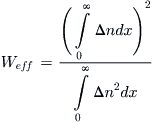 (18)
(18)
This effective width for the carrier density distribution allows one to transform a measurement of bulk thick silicon into a standard wafer measurement, as far as the lifetime analysis is concerned. The total carrier concentration is then the product of navg and Weff:
 (19)
(19)
The above functions can be determined by computer simulation of the carrier density profile, which is dependent on the diffusion length in the material as well as the distribution of light wavelengths incident on the sample. The problem can also be solved analytically for the important case of steady-state illumination with monochromatic light and infinite surface recombination [39]:
![]() (20)
(20)
![]() (21)
(21)
where L is the diffusion length of carriers in the sample and α is the absorption coefficient for the light. Equation (20) permits the calculation of the bulk lifetime of thick samples based on the measurement of effective lifetime at a specific wavelength. It indicates that the measured effective lifetime is a lower bound on the bulk lifetime, which can approach the bulk lifetime only for absorption depths in the silicon that are greater than the carrier diffusion length in the material. Equation (21) offers a figure of merit for the practical sensors, which should ideally have a sensing depth exceeding Weff.
Another special case of interest is the transient decay that follows the termination of an initial steady-state illumination, essentially a PCD measurement using a long excitation pulse. In this case, the effects of surface recombination diminish with time after the excitation pulse is extinguished, as the carriers diffuse deeper into the silicon bulk. The carrier lifetime will asymptotically approach the actual bulk lifetime after the surface becomes depleted of excess carriers. Since the effective width in this case is changing with time, the average carrier density, given by Equation (17), needs to be evaluated numerically [39,40]. The ability of a given instrument to measure the true bulk lifetime depends on its sensing depth, as the carrier density profile moves into the bulk away from the sensor. The advantage of the transient method for measuring bulk lifetimes is that it is far less sensitive to the surface recombination velocity than the steady-state approach.
3.4 Lifetime Instabilities and Measurement Artifacts
3.4.1 Lifetime Changes in Boron-Doped CZ Silicon and Iron-Contaminated Silicon
For p-type silicon wafers, the lifetime can change pronouncedly upon illumination or heating. It is important to be aware of the possibility of lifetime instabilities while performing measurements; on the other hand, such changes constitute useful tools for process diagnosis, particularly to check for contamination. Two especially significant cases of carrier lifetime instability have been documented extensively and are described here as examples: one is due to the presence of iron, the other to the presence of oxygen, both forming complexes with boron. While iron is avoidable, oxygen is innate to CZ grown silicon (except advanced CZ methods using magnetic confinement of the melt), which typically has an oxygen concentration in the vicinity of 7×1017 cm−3. The effect only occurs when both boron and oxygen are present, and is more severe the higher the concentration of both [41]. The conversion efficiency of 1-Ωcm CZ silicon cells has been reported to degrade by 4% relative after about 50 hours of one-sun illumination, while for 0.45 Ωcm the degradation is greater (about 7.5%), and for 10 Ωcm it is lower (1% or less). The lifetime of typical 1-Ωcm boron-doped silicon degrades by more than a factor of ten after 5 hours of exposure to one-sun illumination, approaching a final lifetime of 10–20 μs [42]. Recent work has focused on methods that have been found to put this defect into a seemingly stable, low-recombination state by use of certain temperature-illumination histories [43].
Similar levels of efficiency degradation of 3-4% relative (about 0.5% absolute) after 30 minutes, one-sun illumination can occur due to the presence of iron [44]. The change in lifetime upon exposure is a well established method to determine the concentration of interstitial iron in silicon [45]. There are, however, significant differences between FeB pairs and BO complexes: (1) in the case of Fe, an anneal at 210°C degrades the lifetime in low injection, in much the same way as illumination [46], whereas in the case of BO complexes, the lifetime recovers after annealing at moderate temperatures. (2) The shape of the injection level dependent lifetime curve changes differently: the curves before and after degradation cross over in the case of Fe and FeB (see Figure 1), while they remain approximately parallel in the case of BO. (3) An additional differentiating feature is that the lifetime of Fe contaminated silicon recovers after long-term storage in the dark, whereas that of BO-limited silicon does not.
3.4.2 High Apparent Lifetime at Low Excess Carrier Densities
In some cases an abnormally high apparent lifetime is observed at very low carrier densities. The phenomenon affects transient-decay and steady-state photoconductance measurements, as well as infrared absorption or emission, but not photo or electro-luminescence measurements [47]. The abnormality is evidenced by a strong increase of the apparent lifetime as the carrier injection level decreases. For some materials, particularly multicrystalline silicon, the effect can obscure the true carrier recombination even in the carrier-density range corresponding to the operating point for solar cells, generally between 1×1013 cm−3 and 1×1015 cm−3. This behavior can be due to three different physical mechanisms, the trapping of minority carriers [48], grain boundary potentials that impede lateral conductance in the dark [49,50], or, in samples with junctions, Depletion Region Modulation [51,52]. For many practical situations, simple corrections can be used to retrieve the actual recombination lifetime [53].
4 Relationship between Device Voltage and Carrier Lifetime
The output voltage of a solar cell is principally determined by the excess minority-carrier density at the junction edge of the quasi-neutral base region, defined to be at the plane x = 0 in the following approximate expression:
![]() (22)
(22)
In open-circuit conditions, this minority-carrier density is the result of a balance between photogeneration and recombination. The conditions are identical to those of the steady-state method to measure the lifetime, described in Section 3. It is therefore possible to obtain Δn from a photoconductance measurement and determine an implicit, or expected voltage. Complete characteristic curves can be obtained by plotting the implicit voltage as a function of the illumination, expressed in unit of suns (1 sun = 1 kW/m2).
Direct measurements of the voltage are possible as soon as a junction exists in the wafer. By taking data at a range of illumination intensities, Suns–Voc curves can be constructed and analyzed to obtain diode saturation currents, ideality factors, shunts and ideal efficiencies [54]. Applications of this are shown in Section 5. A generalized expression to obtain the Suns–Voc curves from voltage measurements under quasi–steady-state illumination or during a transient open-circuit decay (OCVD) has also been developed [55].
Conversely, solving for Δn as a function of voltage and substituting this value in Equation (7) converts any voltage measurement into an effective lifetime value. Note that the equation for the lifetime uses an average carrier density, which in some cases can be substantially lower than the value of Δn(0) obtained from the voltage through Equation (22) [37]. Temperature control, knowledge of the intrinsic carrier density ni, and the dopant density are necessary to obtain the lifetime from a voltage measurement, and vice versa. In contrast, photoconductance lifetime measurements require knowledge of carrier mobilities and are relatively insensitive to temperature.
Photoluminescence can provide a contactless probe of the electrochemical potential, or implicit voltage, within a sample, since the PL signal is proportional to the left-hand side of Equation (22). This method, sometimes called Suns–PL [56], is analogous to the Suns–Voc methodology described earlier, without requiring junction formation or probing.
5 Applications to Process Monitoring and Control of Silicon Solar Cells
In-process monitoring of the electronic properties of the silicon wafer using minority-carrier measurements has been extensively used for high-efficiency solar cell optimization at research laboratories, and this can be useful for industrial production environments as well. Several possible industrial process-control applications are detailed below for single- and multicrystalline solar cells. The main electronic properties to be measured include resistivity, carrier lifetime, and device voltage. It is possible to measure the resistance of the substrate, doped layers, and metallization at each stage in the process. The effective lifetime of minority carriers in the silicon can also be monitored at each stage using, for example, photoconductance measurements, or via calibrated PL images. Finally, after junction formation, measurements can be made of the voltage, which is a clear indicator of final device performance.
5.1 Resistivity Measurements
The resistivity of the silicon bulk material can be measured at the ingot or wafer levels using contacting or noncontacting arrangements [14,57]. Knowledge of the resistivity and, subsequently, the net doping density, is very important in the optimization of the fabrication process and the interpretation of solar cell performance, since both the voltage and the current depend on it. The lifetime and diffusion length are also correlated to the resistivity of the substrate, with lower resistivities usually being accompanied by lower lifetimes. A higher resistivity, on the other hand, makes the device more dependent on the quality of the surfaces.
Given that residual iron is almost omnipresent in solar grade silicon, and interstitial iron forms pairs with ionized acceptors at a rate that is proportional to the acceptor concentration, techniques based on lifetime testing have also been developed to accurately determine the acceptor concentration in p-type silicon [58].
The sheet resistance of the emitter (usually phosphorus) diffusion is another essential control parameter. It is correlated to the dopant density profile, which determines the emitter saturation current density, the emitter quantum efficiency, the contact resistance properties, and the tolerance to shunt formation during firing. The sheet resistance can be measured by the four-point-probe method [14] or by contactless inductive coupling [10] if the wafer bulk resistivity is subtracted. Resistance measurements can also be used to monitor the thickness of metal deposited at the rear of the wafers (an alternative is to measure the weight differential) and the resulting alloying of the aluminum to form a highly doped p-type BSF layer.
5.2 Process Monitoring via Lifetime Measurements
In R&D laboratories, most of the fabrication steps can be characterized in detail using lifetime measurements. Frequently, such detailed studies are done under ideal conditions to achieve unambiguous results. For example, investigations of mc-Si wafers versus position in the original cast brick have often been made by etching off the surface and subsequently applying a high-quality surface passivation, in order to determine the effect of each process step on bulk lifetime without confounding effects of the surface [59,60]. Alternatively, the surface can be etched back and then passivated using a liquid, such as HF [61] or iodine in ethanol [60,62]. Satisfactory low-temperature passivation has also been obtained with corona-charged photoresist [63] and polymer films [64]. Many studies have also been performed on wafers with the surfaces as they exist after each step in the process [65,66]. Such measurements do not require special wafer preparation and are ideal for industrial process control in production lines. Especially on multicrystalline material, high-resolution mapping of the wafer has been used to identify the response of different grains and grain boundaries to gettering and hydrogenation [67,68]. These spatially resolved methods include microwave-PCD (μ-PCD), modulated free-carrier absorption, EL and PL, surface photovoltage, IR carrier density imaging, microwave phase-shift techniques and light beam induced current (LBIC) [69].
5.2.1 Measurements of Carrier Lifetime in an Ingot or Brick
Cast mc-Si ingots usually present a low minority-carrier lifetime near the top, bottom and side surfaces, due to contact with the crucible and impurity segregation. Once the ingot is sawn into bricks, the minority-carrier lifetime is usually mapped in order to determine the region of potentially good wafers. Two-dimensional high-resolution μ-PCD measurements have often been used to characterize mc-Si bricks and CZ ingots using commercially available instruments. More recently, QSSPC as well as Photoluminescence techniques have been applied to measure carrier lifetimes in bricks [39,70]. The initial lifetimes for as-grown material are, however, not perfectly correlated with final solar cell efficiency. It has been shown, for example, that some regions of cast bricks that might be discarded based on initial lifetime measurements recover lifetime during the high-temperature steps in cell processing due to gettering effects [66,71]. Many of these low lifetime regions can also result in good solar cells after hydrogen bulk passivation procedures. Despite these complexities, a better understanding of the initial silicon lifetime and the effects of the process on the various regions of ingots and bricks is expected to result in better strategies for optimizing the silicon growth and choosing the regions of silicon to submit to the expensive sawing, wafer cleaning, and cell fabrication processes. Rejecting material at this early stage has great value. Tight tolerances for incoming wafers at the beginning of cell fabrication will also permit better optimization and control of the fabrication process.
5.2.2 Lifetime Measurements on Bare Wafers
In principle, measurements on bare wafers should not be necessary if the ingot or the brick has been measured prior to sawing. In practice, a measurement at the wafer level can indicate if a sufficient thickness of silicon was removed at the saw-damage etch step. In addition, many silicon solar cell manufacturers do not fabricate the wafers, but purchase them, and it is of great interest for both the vendor and the manufacturer to have the capability to measure the minority-carrier lifetime of the individual bare wafers. This is not simple, since the measured effective lifetime of a wafer without surface passivation can be very low.
For typical commercial solar cells, the efficiency is relatively constant for bulk lifetimes greater than 5 μs, corresponding to diffusion lengths greater than 116 μm. Therefore, the main point of a lifetime measurement at the stage of bare wafers is to determine if the wafer has a minimum required lifetime of 2–5 μs. Wafers with greater lifetime than this clearly “pass” and wafers with lower lifetime “fail.” This type of pass/fail test is possible even in the absence of surface passivation by using infrared light, as discussed in section 3.2. This methodology has been discussed in detail in several recent publications [32] in which a one-to-one correlation was shown between the measured bulk lifetimes and the final cell efficiencies. Photoluminescence imaging has also been applied to wafer sorting, using the spatial resolution of lifetime to give information on the defect distribution across the wafer [72].
As seen in Figure 2, measurements on bare wafers will generally result in effective lifetimes in the range of 0.1 to 2 μs. When using methods subject to trapping-like effects, the low levels of photoconductance corresponding to these lifetimes makes it critically important to determine the lifetime with a data analysis that removes the artifacts that come from trapping, as discussed in Section 3.4.2. Due to the dependence of the lifetime on injection level described in Section 2, all measurements of lifetime should be performed at the same minority-carrier injection level. This injection level should preferably be chosen to be relevant to the maximum power operating point of the finished solar cell.
5.2.3 Effective Lifetime After Emitter Formation
An ideal point to measure the effective lifetime is after forming the emitter, since at this stage it can represent a close prediction of the final solar cell efficiency. The emitter region of a solar cell, usually formed by a phosphorus diffusion, acts as a surface passivation. Amorphous silicon heterojunction technology (a-Si:H) offers an even clearer, and frequently more effective, example of surface passivation. In normal operating conditions of low injection, an emitter region is seen from the base of the cell as a surface recombination velocity, whose value is determined by the emitter-saturation current density Joe that characterizes recombination losses within the emitter region (see Section 3.2.2). This correspondence between SRV and Joe is shown in Figure 2 for a 1-Ωcm p-type wafer. It can be noted that Joe values below 10−12 Acm−2 provide a reasonable passivation (SRV<1000 cm/s). Yet such Joe = 10−12 Acm−2 would limit the measurable effective lifetime to approximately 12 μs in 1-Ωcm material, even if the bulk lifetime may be much higher. It should be noted that such limit is less restrictive for higher resistivity wafers. This surface-like role of the emitter regions applies to both aluminum-alloyed BSF regions and to phosphorus- or boron-diffused regions, as well as to a-Si:H heterojunctions. Representative values for industrial phosphorus (n+ region) and aluminium (p+ region) diffusions are 8×10⁻¹³ Acm−2 and 5×10⁻¹³ Acm−2, respectively.
The techniques discussed in Section 3.2.2 can be applied to determine both the bulk lifetime and the emitter saturation current density. It is advisable to use special test wafers with a lower substrate doping to maximize the range of carrier injection data that can be used for the analysis and extend the range of Joe values that can be determined. Once Joe is measured, its contribution to the low injection range of the effective lifetime can then be subtracted. Therefore data taken in two minority-carrier density injection ranges allow both the bulk lifetime in the relevant range of cell operation and the emitter saturation current density to be uniquely determined. The exact analysis will depend on the technology used for the emitter formation, since this step may result on a diffused or heterojunction region at the front only, or at both surfaces. If emitter-surface passivation is done in a subsequent, the same methodology discussed above can be used to determine the improvements to the bulk lifetime and the emitter saturation current density that may result from that process step. This provides an ideal way to characterize the effectiveness of emitter passivation by, for example, oxidation, silicon nitride deposition, or Al2O3 deposition.
5.3 Device-Level Characterization
The most common characterization used in industry consists of the final I-V curve test of the solar cell under simulated one-sun illumination, sometimes supplemented by a measurement of the I-V curve in the dark. A classical interpretation of these measurements with the traditional double-exponential model leads to the determination of saturation current densities, ideality factors, and shunt and series resistances. These methods are, nevertheless, of limited usefulness as a diagnostic and control tool. In the past, research laboratories have used Isc–Voc measurements to gain further insight into the device. Very early in the history of solar cell development, it was realized that the Isc–Voc curve contained information about the fundamental diode characteristic free from series resistance effects [73]. The Suns–Voc method [74] is a convenient implementation of the same idea, where the device is kept in open-circuit at all times, but its short-circuit current is not actually measured. Instead, the incident light intensity, which varies with time in a quasi–steady-state fashion, is measured with a calibrated reference solar cell. New methods for determining the local series and shunt resistances as well as the local saturation current density, to produce an image of these parameters across the surface of the solar cell, have been developed recently. A selection of them is described below.
5.3.1 Standard Diode Analysis of Suns–Voc Curves
Suns–Voc measurements are possible early in the fabrication process, by probing the wafer after junction formation. This allows the qualification of basic materials and device properties in terms of potential device performance, before the “back-end” processing may complicate the interpretation. The illumination intensity can be expressed in units of standard solar irradiance, that is, Suns, or converted to units of current by using as a scaling factor either the short-circuit current of the cell (if it has been measured separately) or an estimate of it based on the modeled photogeneration in the sample.
An example of Suns–Voc data is shown in Figure 4 in the form of the standard semi-logarithmic diode characteristic curve. Process control using the analysis of Figure 4 should optimize the voltage at 0.05 to 0.1 suns, corresponding to the maximum power operating voltage of the solar cell. Similarly to dark I–V curves, Suns–Voc curves can be interpreted by means of a recombination current density and a shunt resistance. The data in Figure 4 can be separated into recombination and shunt current densities, as shown in the plots. The recombination current is usually expressed, following Shockley’s terminology, as a pre-exponential factor called the saturation current density and an exponential term of the junction voltage affected by an ideality factor. It is important to realize that the saturation current density obtained from the analysis of I–V or Suns–Voc curves is a global parameter that reflects all the recombination processes within the device, encompassing recombination within the emitter and base regions, as well as at the surfaces and within any space charge regions. Another important observation is that, whereas a satisfactory fit to the data is usually possible using a double-exponential model, the transition from ideality 1 to 2 (or greater) factors is often due to the variability of the bulk lifetime or the surface recombination velocity [75], and not to recombination in the space charge region. In the case shown in Figure 4, the deviation from unity ideality factor can be attributed to the B:O defect, which produces lower lifetimes at lower carrier density.
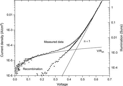
FIGURE 4 Suns–Voc measurement of a p-type CZ monocrystalline silicon solar cell plotted in a semi-logarithmic scale, with a separation into components due to the shunt and the diode recombination current. A line for the ideal diode equation with unity ideality factor is shown for reference. The measured data is illumination (right scale) vs. voltage. The left scale is constructed from (Suns ∗ Jsc).
5.3.2 Monitoring Contact Formation
Measuring the contact resistance between the metal and the semiconductor usually requires separate experiments and special test structures. The Corescan instrument [76] provides detailed information about the contact resistance and the emitter sheet resistance on the finished solar cell. The technique, which is destructive, is based on scanning a probe directly on the silicon and the metal fingers to map the voltage drop versus position across the illuminated solar cell. Such voltage maps can be used to optimize the front-grid metallization and diagnose metal contact problems [77].
The metallization and sintering process steps can also be monitored for voltage loss, shunts, and contact problems using the Suns–Voc technique. Although not immediately obvious, data taken under open-circuit conditions can be valuable for monitoring the properties of the solar cell contacts. Metal contacts can be modeled as a Schottky potential barrier, which is formed by most metals on silicon, in parallel with some form of leakage current. The leakage might be from the metal locally doping or spiking the silicon or from thermally assisted tunneling through the potential barrier. Under one-sun conditions, for a well-formed contact, the Schottky barrier is effectively shorted by the leakage. However, on a poorly formed contact at a sufficiently high light intensity the Schottky diode will build up a voltage opposing the junction voltage by generating a current that the leakage is unable to fully shunt. Another example is when aluminum is used to penetrate through a phosphorus diffusion on the back of the solar cell. Insufficient firing of the Al results in an opposing voltage at high light intensities from the parasitic back p–n junction. Schottky type contacts usually result in low fill factors and efficiencies. This poor contact effect is indicated as an ideality factor less than unity for the global solar cell, or even a voltage that decreases at high-illumination intensity. By monitoring the open-circuit voltage at light intensities significantly higher than the nominal operating conditions, this effect can be used to anticipate and solve problems in the contact formation. This method is both a good diagnostic and a process optimization technique [78].
5.3.3 Fill Factor and Series Resistance Measurements
The global series resistance of the device can be measured by a number of methods. It is important to emphasize that not all them provide the relevant value of series resistance. Methods based on measurements of the device under illumination are more realistic than measurements in the dark [79]. Wolf and Rauschenbach [73] described how a comparison of Isc–Voc data with the final I-V curve of the solar cell can then be used to determine the series resistance very precisely. They also demonstrated a method based on measuring the I-V curve at two or more different illumination intensities. An experimental comparison between these methods, plus the Suns–Voc method described below, can be found in reference [80].
An alternative presentation of Suns–Voc data is shown in Figure 5. By using the superposition principle, a photovoltaic pseudo I–V curve can be constructed from the open-circuit voltage measurements of Figure 4. At each value of the voltage, the pseudo, or implied current is given by
![]() (23)
(23)
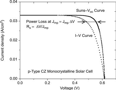
FIGURE 5 The same Suns–Voc data as in Figure 4, plotted as a photovoltaic pseudo I–V curve and compared to the actual I–V curve taken on the finished solar cell.
This yields the familiar photovoltaic I-V curve format, permitting the customary interpretation of fill factor, efficiency and shunt. The parameters that matter most to solar cell performance are now visually obvious. For example, it can immediately be seen if the shunt is having a major effect on the maximum power point or not, and the upper bound on fill factor and efficiency (without series resistance effects) is clearly displayed.
Eventually, by comparing the Suns–Voc curve with the actual output I–V curve of the finished solar cell, the series resistance can be determined with precision. Since the pseudo I–V curve from Suns–Voc has the shunt and ideality factors fully included, the differences between the two curves can be clearly attributed to series resistance. The latter is simply given by the voltage difference between the two curves at the knee, in the vicinity of the maximum power point, divided by the current. As an example, the same data in Figure 4 are shown in Figure 5. The curves follow each other except near the maximum power point, where series resistance effects are greater. The solar cell in Figures 4 and 5 has a large series resistance loss that would generally imply that different parts of the solar cell are operating at different voltages at the maximum power point. This can complicate the separation of the diode recombination current from series resistance and shunting. The use of the Suns–Voc curve to obtain the diode characteristics and the shunting independently from series resistance effects is especially useful under these circumstances. Electroluminescence imaging [19] can provide similar information as the Suns–Voc data, with the added feature of being spatially resolved, since the luminescence signal measured is proportional to the junction voltage. Photoluminesence can provide similar information to the EL signal, but more weighted toward the average bulk lifetime rather than the junction voltage. Due to the fact that the current flow in the device is different during an EL and PL measurement, a comparison between both can be used to give information on the series resistance in the device. In addition, PL measurements at two different operating conditions can be used to produce a high-resolution map of series resistance [72].
6 Conclusions
Characterizing material quality and monitoring the impact of each fabrication step is crucial for the PV industry to develop high efficiency solar cell technologies. A broad range of characterization techniques has been developed in recent years, many of them fast enough for in-line process control. The advent of advanced techniques that give a detailed image of the electronic quality of silicon ingots, wafers, and devices provides a wealth of information. More than ever, it is imperative to interpret such information with sound physics to understand the limitations and applicability of each technique. In this chapter the common principles underlying the most important characterization methods has been outlined and possible applications of these methods to monitoring solar cell fabrication have been described. This review is not exhaustive, but should be sufficient to illustrate the range of options available for silicon material, surface, and device characterization, a range that can be expected to broaden in the future.
Acknowledgements
The authors would like to thank Keith Forsyth for the data presented in Figures 4 and 5.
References
1. Rein S, Rehrl T, Warta W, Glunz SW. Lifetime spectroscopy for defect characterization: systematic analysis of the possibilities and restrictions. J Appl Phys. 2002;91:2059.
2. Macdonald D, Cuevas A, Wong-Leung J. Capture cross sections of the acceptor level of iron-boron pairs in p-type silicon by injection-level dependent lifetime measurements. J Appl Phys. 2001;89:7932.
3. Kerr MJ, Cuevas A. General parameterization of Auger recombination in crystalline silicon. J Appl Phys. 2002;91:2473.
4. Stevenson DT, Keyes RJ. Measurement of carrier lifetimes in germanium and silicon. J Appl Phys. 1955;26:190.
5. Bube RH. Photoconductivity of Solids. New York: Wiley; 1960;.
6. Sinton RA, Cuevas A. Contactless determination of current-voltage characteristics and minority-carrier lifetimes in semiconductors from quasi–steady-state photoconductance data. Appl Phys Lett. 1996;69:2510.
7. Nagel H, Berge C, Aberle A. Generalized analysis of quasi–steady-state and quasi- transient measurements of carrier lifetimes in semiconductors. J Appl Phys. 1999;86:6218.
8. Klaassen DBM. A unified mobility model for device simulation—I Model equations and concentration dependence. Solid-State Electron. 1992;35:953.
9. ASTM, Designation F-28–75. Measuring the Minority Carrier Lifetime in Bulk Germanium and Silicon. American Society for Testing of Materials 1981;.
10. Miller GL, Robinson DAH, Wiley JD. Contactless measurement of semiconductor conductivity by radio frequency free carrier power absorption. Rev Sci Instrum. 1976;47:799.
11. Deb S, Nag BR. Measurement of carriers in semiconductors through microwave reflection. J Appl Phys. 1962;33:1604.
12. Kunst M, Beck G. The study of charge carrier kinetics in semiconductors by microwave conductivity measurements. J Appl Phys. 1986;60:3558.
13. Schofthaler M, Brendel R. Sensitivity and transient response of microwave reflection measurements. J Appl Phys. 1995;77:3162.
14. Schroder DK. Semiconductor Material, Device, Characterization. third ed. John Wiley and Sons 2006.
15. Harrick NJ. LIfetime measurements of excess carrier kinetics in semiconductors. J Appl Phys. 1956;27:1439.
16. Glunz SW, Warta W. High resolution lifetime mapping using modulated free- carrier absorption. J Appl Phys. 1995;77:3243.
17. Brendel R, Bail M, Bodman B. Analysis of photoexcited charge carrier density profiles in Si wafers by using an infrared camera. Appl Phys Lett. 2002;80:437.
18. Isenberg J, Riepe S, Glunz SW, Warta W. Imaging method for laterally resolved measurement of minority carrier densities and lifetimes: measurement principle and first applications. J Appl Phys. 2003;93:4268.
19. Fuyuki T, Kondo H, Yamazaki T, Takahashi Y, Uraoka Y. Photographic surveying of minority carrier diffusion length in polycrystalline silicon solar cells by electroluminescence. Appl Phys Lett. 2005;86:262108.
20. Wurfel P, Trupke T, Puzzer T, Schaffer E, Warta W, Glunz SW. Diffusion lengths of silicon solar cells from luminescence images. J Appl Phys. 2007;101:123110.
21. Trupke T, Bardos RA, Abbott MD. Self-consistent calibration of photoluminescence and photoconductance lifetime measurements. Appl Phys Lett. 2005;87:184102.
22. Trupke T, Bardos RA, Schubert MC, Warta W. Photoluminescence imaging of silicon wafers. Appl Phys Lett. 2006;89:044107.
23. Basore PA. Extended spectral analysis of internal quantum efficiency. Louisville: 23rd IEEE Photovoltaic Specialists Conference; 1993; p. 147.
24. Brendel R, Wolf M. Differential and actual surface recombination velocities. Nice: 13th European Photovoltaic Solar Energy Conference; 1995; p. 428.
25. Schmidt J. Measurement of differential and actual recombination parameters on crystalline silicon wafers. IEEE Trans Electron Dev. 1999;46:2018.
26. SEMI PV9-1110—Test method for excess charge carrier decay in PV silicon materials by non-contact measurements of microwave reflectance after a short illumination pulse. 2010.
27. Lauer K, Laades A, Ubensee H, Metzner H, Lawerenz A. Detailed analysis of the microwave-detected photoconductance decay in crystalline silicon. J Appl Phys. 2008;104:104503.
28. Aberle AG, Robinson SJ, Wang A, Zhao J, Wenham SR, Green MA. High- efficiency silicon solar cells: fill factor limitations and non-ideal diode behaviour due to voltage-dependent rear surface recombination velocity. Prog Photovoltaics. 1993;1:133.
29. Gandhi SK. Semiconductor Power Devices. Wiley Intersicence 1977.
30. Brody J, Rohatgi A, Ristow A. Review and comparison of equations relating bulk lifetime and surface recombination velocity to effective lifetime measured under flash lamp illumination. Sol Energy Mater Sol Cells. 2003;77:293.
31. Basore PA, Clugston DA. PC1D V5.3. Sydney, Australia: University of New South Wales; 1998.
32. Bothe K, Krain R, Falster R, Sinton R. Determination of the bulk lifetime of bare multicrystalline silicon wafers. Prog Photovoltaics. 2010;18:204.
33. Bail M, Brendel R. Separation of bulk and surface recombination by steady state photoconductance measurements. Glasgow: 16th European PVSEC; 2000; p. 98.
34. Cuevas A. The effect of emitter recombination on the effective lifetime of silicon wafers, Sol Energy Mater Sol. Cells. 1999;57:277.
35. Reichel C, Granek F, Benick J, Schultz-Wittmann O, Glunz SW. Comparison of emitter saturation current densities determined by injection-dependent lifetime spectroscopy in high and low injection regimes. Prog Photovoltaics Res Appl. 2010; n/a.
36. Kane DE, Swanson RM. Measurement of the emitter saturation current by a contactless photoconductivity decay method. Las Vegas: 18th IEEE PVSC; 1985; p. 578.
37. Cuevas A, Sinton RA. Prediction of the open-circuit voltage of solar cells from the steady-state photoconductance. Prog Photovoltaics. 1997;5:79.
38. Bowden S, Sinton RA. Determining lifetime in silicon blocks and wafers with accurate expressions for carrier density. J Appl Phys. 2007;102:124501.
39. Swirhun JS, Sinton RA, Forsyth MK, Mankad T. Contactless measurement of minority carrier lifetime in silicon ingots and bricks. Prog Photovoltaics Res Appl. 2010; n/a.
40. Schüler N, Hahn T, Dornich K, Niklas JR, Gründig-Wendrock B. Theoretical and experimental comparison of contactless lifetime measurement methods for thick silicon samples. Sol Energy Mater Sol Cells. 2010;94:1076.
41. Schmidt J, Aberle AG, Hezel R. Investigation of carrier lifetime instabilities in Cz-grown silicon. Washington: 26th IEEE Photovoltaic Specialists Conference; 1997; p. 13.
42. Glunz SW, Rein S, Warta W, Knobloch J, Wettling W. On the degradation of CZ-silicon solar cells. Vienna: 2nd World Conference on Photovoltaic Energy Conversion; 1998; p. 1343.
43. Herguth A, Hahn G. Kinetics of the boron-oxygen related defect in theory and experiment. J Appl Phys. 2010;108:114509.
44. Reis JH, King RR, Mitchell KW. Characterization of diffusion length degradation in Czochralski silicon solar cells. Appl Phys Lett. 1996;68:3302.
45. Macdonald D, Geerligs LJ, Azzizi A. Iron detection in crystalline silicon by carrier lifetime measurements for arbitrary injection and doping. J Appl Phys. 2004;95:1021.
46. Zoth G, Bergholz W. A fast, preparation-free method to detect iron in silicon. J Appl Phys. 1990;67:6764.
47. Bardos RA, Trupke T, Schubert MC, Roth T. Trapping artifacts in quasi– steady-state photoluminescence and photoconductance lifetime measurements on silicon wafers. Appl Phys Lett. 2006;88:053504.
48. Macdonald D, Cuevas A. Trapping of minority carriers in multicrystalline silicon. Appl Phys Lett. 1999;74:1710.
49. Maruska HP, Ghosh AK, Rose A, Feng T. Hall mobility of polycrystalline silicon. Appl Phys Lett. 1980;36:381.
50. Sinton RA, Swirhun J, Forsyth M, Mankad T, Nyhus J, Camel L. The effects of subbandgap light on QSSPC measurements of lifetime and trap density: what is the cause of trapping?. Valencia: Proceedings of the 25th European Photovoltaic Solar Energy Conference; 2010.
51. Bail M, Schulz M, Brendel R. Space-charge region-dominated steady-state photoconductance in low-lifetime Si wafers. Appl Phys Lett. 2003;82:757.
52. Cousins PJ, Neuhaus DH, Cotter JE. Experimental verification of the effect of depletion-region modulation on photoconductance lifetime measurements. J Appl Phys. 2004;95:1854.
53. Macdonald D, Sinton RA, Cuevas A. On the use of a bias-light correction for trapping effects in photoconductance-based lifetime measurements in silicon. J Appl Phys. 2001;89:2772.
54. Sinton RA, Cuevas A. A quasi–steady-state open-circuit voltage method for solar cell characterization. Glasgow, Scotland: 16th European PVSEC; 2000; p. 1152.
55. Kerr MJ, Cuevas A, Sinton RA. Generalized analysis of quasi–steady-state and transient decay open circuit voltage measurements. J Appl Phys. 2001;91:399.
56. Trupke T, Bardos RA, Abbott MD, Cotter JE. Suns-photoluminescence: contactless determination of current-voltage characteristics of silicon wafers. Appl Phys Lett. 2005;87:093503.
57. Sinton RA, Cuevas A, Stuckings M. Quasi–steady-state photoconductance, a new method for solar cell material and device characterization. Washington, D.C., U.S.A.: Proceedings of the 25th Photovoltaic Specialists Conference; 1996; p. 457.
58. Macdonald D, Cuevas A, Geerligs LJ. Measuring dopant concentrations in compensated p-type crystalline silicon via iron-acceptor pairing. Appl Phys Lett. 2008;92:202119.
59. Macdonald D, Cuevas A, Ferrazza F. Response to phosphorus gettering of different regions of cast multicrystalline silicon ingots. Solid-State Electron. 1999;43:575.
60. Rohatgi A, Yelundur V, Jeong J, et al. Aluminium-enhanced PECVD SiNx hydrogenation in silicon ribbons. Glasgow, U.K: Proceedings of the 16th European Photovoltaic Solar Energy Conference; 2000; p. 1120.
61. Yablonovitch E, Allara DL, Chang CC, Gmitter T, Bright TB. Unusually low surface-recombination velocity on silicon and germanium substrates. Phys Rev Lett. 1986;57:249.
62. Horanyi TS, Pavelka T, Tutto P. In situ bulk lifetime measurement on silicon with a chemically passivated surface. App Surf Sci. 1993;63:306.
63. Schmidt J, Aberle AG. Easy-to-use surface passivation technique for bulk carrier lifetime measurements on silicon wafers. Prog Photovoltaics. 1998;6:259.
64. Biro D, Warta W. Low temperature passivation of silicon surfaces by polymer films. Sol Energy Mater Sol Cells. 2002;71:369.
65. Stocks M, Cuevas A, Blakers A. Process monitoring of multicrystalline silicon solar cells with quasi–steady state photoconductance measurements. Anaheim: Proceedings of the 26th IEEE Photovoltaic Specialists Conference; 1997; p. 123.
66. Coletti G, Iuliis SD, Ferrazza F. A new approach to measure multicrystalline silicon solar cells in a production process. 17th European Photovoltaic Solar Energy Conference 2001; p. 1640.
67. Geiger P, Kragler G, Hahn G, Fatch P, Bucher E. Spatially resolved lifetimes in EFG and string ribbon silicon after gettering an hydrogenation steps. New Orleans: 29th IEEE Photovoltaic Specialists Conference; 2002.
68. Tan J, Cuevas A, Macdonald D, Trupke T, Bardos R, Roth K. On the electronic improvement of multi-crystalline silicon via gettering and hydrogenation. Prog Photovolt Res Appl. 2008;16:129.
69. Warta W. Defect and impurity diagnostics and process monitoring. Sol Energy Mater Sol Cells. 2002;72:389.
70. Trupke T, Nyhus J, Sinton R, Weber JW. Photoluminescence imaging on silicon bricks. Hamburg: 24th European Photovoltaic Solar Energy Conference; 2009; p. 1029.
71. Cuevas A, Macdonald D, Kerr MJ, et al. Evidence of impurity gettering by industrial phosphorus diffusion. Anchorage, Alaska: 28th IEEE Photovoltaic Specialists Conference; 2000; p. 108.
72. Kampwerth H, Trupke T, Weber JW, Augarten Y. Advanced luminescence based effective series resistance imaging of silicon solar cells. Appl Phys Lett. 2008;93:202102.
73. Wolf M, Rauschenbach H. Series resistance effects on solar cell measurements. Adv Energy Convers. 1963;3:455.
74. Sinton RA, Cuevas A. A quasi-steady open-circuit voltage method for solar cell characterisation. Glasgow, U.K: Proceedings of the 16th European Photovoltaic Solar Energy Conference; 2000; p. 1152.
75. MacDonald D, Cuevas A. Reduced fill factors in multicrystalline silicon solar cells due to injection-level dependent bulk recombination lifetimes. Prog Photovoltaics. 2000;8:363.
76. van der Heide ASH, Schonecker A, Wyers GP, Sinke WC. Glasgow: 16th European Photovoltaic Solar Energy Conference; 2000; p. 1438.
77. van der Heide ASH, Bultman JH, Hoornstra J, Schonecker A, Wyers GP, Sinke WC. Optimizing the front side metallization process using the Corescan. New Orleans: 29th IEEE Photovoltaic Specialists Conference; 2002.
78. Glunz SW, Nekarda J, Mäckel H, Cuevas A. Analyzing back contacts of silicon solar cells by Suns–Voc measurement at high illumination densities. Milan, Italy: 22nd European Photovoltaics Solar Energy Conference; 2007; p. 849.
79. Araujo GL, Cuevas A, Ruiz JM. Effect of distributed series resistance on the dark and illuminated characteristics of solar cells. IEEE Trans Electron Dev ED-33 1986;391.
80. Pysch D, Mette A, Glunz SW. A review and comparison of different methods to determine the series resistance of solar cells. Sol Energy Mater Sol Cells. 2007;91:1698.