Chapter IC-5
High-Efficiency Back-Contact Silicon Solar Cells for One-Sun and Concentrator Applications
Chapter Outline
2. Concentrator Applications of IBC Solar Cells
3. Back-Contact Silicon Solar Cells
3.2. Front-Surface-Field, Tandem-Junction, and Point-Contact Solar Cells
4. Modelling of Back-Contact Solar Cells
5. Perimeter and Edge Recombination
6. Manufacturing Process for Back-Contact Solar Cells
7. Stability of Back-Contact Cells
8. Toward 30% Efficiency Silicon Cells
9. How to Improve the Efficiency of Back-Contact Solar Cells
9.1. Reduce Emitter Saturation Current Density
9.2. Demonstrate Low-Contact Resistance
1 Introduction
Interdigitated back-contact (IBC) silicon solar cells were originally designed for concentrating photovoltaic (CPV) applications. When the first IBC design concept was introduced by R.J. Schwartz [7], the principal objective was to circumvent the limited usage of conventional silicon solar cells with top and bottom contacts for CPV application. In a conventional solar cell design, very low series resistances are difficult to obtain due to the practical sheet resistance of the front-side emitter that must be maintained to keep good quantum efficiency. Therefore, conventional silicon solar cells are not suitable for high concentration ratio—for example, greater than about ×50. Following the introduction of IBC cells and their modelling [7,8], the technology to fabricate such a cell, which required a particularly clean process to maintain high bulk lifetime and low surface recombination velocity, was subsequently developed by the universities of Stanford, Louvain, and Marseilles [4,10,11,19] and later commercialised by companies such as SunPower Corporation [1,2] and Amonix Inc [37]. Over time, the IBC solar cell design became the best silicon solar cell design for CPV applications and, to this date, is still the most efficient one, with efficiencies up to 28.3% in laboratory [2,3].
Although the first applications for IBC solar cells were dense-array and Fresnel lens CPV [1,15], SunPower Corporation also commercialised a version of the IBC solar cell for high-value one-sun applications [13,29–32]. For example, the silicon solar cells powering the Honda Dream solar race car and the NASA Helios unmanned airplane were basically modified and simplified versions of the concentrator IBC solar cells. These solar cells were, however, still too expensive, by more than two orders of magnitude, to be used in flat-plate PV modules for terrestrial applications. A cost-effective flat-plate PV module using IBC silicon solar cells required the development of a low-cost fabrication process, including a simplified process flow [36], lower-cost silicon Czochralski (CZ) substrates, cost-effective lithography steps, and electroplated metallisation [33]. Over the years, the efficiency of one-sun IBC silicon solar cells increased from about 21% to 24.2% [34,35], making its design the most efficiency solar cell design to date for both CPV and one-sun applications in large-volume manufacturing.
2 Concentrator Applications of IBC Solar Cells
Concentrating sunlight for photovoltaic conversion has always been a very attractive solution. Since one can easily acknowledge that the cost of photovoltaic energy conversion is driven by the fabrication cost of the solar cells, particularly the cost of the semiconductor material, it becomes obvious that much less expensive concentrating lenses or mirrors can replace the expensive solar cells area. The concentration ratio can be increased several hundred fold to the point where the cost of fabricating the solar cells becomes a small part (typically 10% to 15%) in the overall PV system cost. However, this benefit does not come without complexity and cost. Concentrating PV systems need solar trackers with a tracking precision that increases with concentration ratio and a more expensive module design with a well-engineered and low-cost passive or active cooling system for the solar cells.
Concentration not only increases the energy productivity of the solar cell material and device but also increases its efficiency, since both current and voltage increase with the light intensity. However, in order to compare efficiencies of concentrator PV systems with flat-plate PV systems, we have to remember that concentrator systems only use direct sunlight, about 85% of the incident power density on a clear sunny day. Therefore, one could think that a 20% efficient concentrator system would produce about the same amount of energy as a 17% efficient flat-plate system if they are both mounted on the same tracking system. However, CPV systems usually benefit from additional advantages—for example, a lower temperature coefficient due to higher voltage—than one-sun solar cells and, in most cases, a lower cell temperature than in flat-plate modules [6].
The series resistance of the cell limits the concentration ratio to which the solar cells can be used and the efficiency advantage of concentration systems over flat plates. To collect a current that is, for example, at a 500× concentration ratio, almost 20 A/cm2 from a solar cell that has an open-circuit voltage of 0.800 V requires a series resistance that is less than 0.001 Ω cm2. To achieve such low series resistance, the concentrator solar cell requires a well-engineered double-level, solderable metallisation scheme [4,5] (see Figure 1).

FIGURE 1 Structure of IBC silicon solar cell.
The carrier recombination in commercial one-sun solar cells for flat-plate application is usually dominated by bulk Shockley–Read–Hall (SRH) or surface recombination. In high-efficiency (>18%) solar cells or when medium-concentration (<100×) is applied, the carrier recombination is usually dominated by junction recombination. Auger recombination usually dominates in very high-concentration silicon solar cells [11]. Auger recombination occurs when an electron from the conduction band recombines with a hole from the valence band, giving its energy to another electron. This is the opposite mechanism of impact ionisation. The Auger recombination rate increases as the cube of the carrier density and is generally the dominant recombination mechanism when the carrier concentration exceeds 1017 cm−3. In order to reduce the Auger recombination rate, concentrator solar cells must be as thin as possible (typically 120 μm or less) and therefore require a good light trapping.
Because the solar cell cost represents only around 10% of the total concentrator PV system cost, a high-efficiency solar cell provides a great leverage for reducing the levelised cost of solar electricity (LCOE); the higher the concentration ratio, the greater the leverage. The most efficient silicon solar cell, both for laboratory cells and for production scale, is currently the IBC and, in particular, the point-contact (PC) solar cell [5–9,37]. The structure of such a cell is shown in Figure 1. It has attained a conversion efficiency of 28.3% [2,3] in the laboratory and 27.6% at 92× (AM1.5D, 10 W/cm2, 25°C) at the production scale [37]. At present, it is the most efficient silicon solar cell for CPV applications. Figures 2 and 3 show examples of concentrator silicon solar cells manufactured by SunPower Corporation of Richmond, California. Two examples of a reflective concentrator dish built by Solar Systems Pty Ltd of Abbotsford, Australia, and using high-efficiency concentrator silicon solar cells, are shown in Figures 4 and 5. The 20-m2 concentrator system represented in Figure 5 was the first silicon-based concentrator system to reach an overall system efficiency of 20% under normal operating conditions [6]. Figure 6 shows a picture of the cells at the receiving point of such a concentrator system in operation.
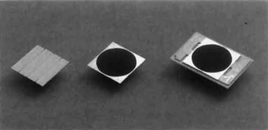
FIGURE 2 A point-contact silicon solar cell for Fresnel concentrator application.
(Courtesy of SunPower Corporation.)

FIGURE 3 A point-contact silicon solar cell for dense-array concentrator application.
(Courtesy of SunPower Corporation.)
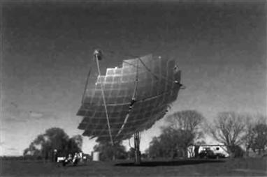
FIGURE 4 Picture of a 25-kW dish concentrating PV system with point-contact silicon solar cells.
(Courtesy of Solar Systems Ply Ltd.)
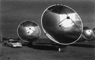
FIGURE 5 A dish concentrating PV system with point-contact silicon solar cells. This PV system, installed in White Cliff, Australia, demonstrated 20% overall efficiency under normal operating conditions [6].
(Courtesy of Solar Systems Ply Ltd.)
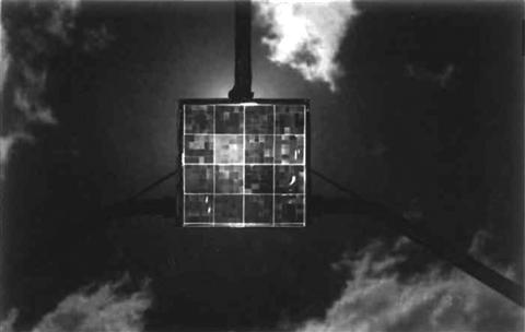
FIGURE 6 A dense-array receiver with point-contact silicon solar cells.
(Courtesy of Solar Systems Ltd Ply.)
3 Back-Contact Silicon Solar Cells
3.1 IBC Solar Cells
Schwartz et al. [7,8] introduced the IBC design in 1975. The main reason that the IBC solar cell design is particularly suitable for high concentration is that both metal contacts are made on the back surface of the cell (Figure 1), so there is no shadowing effect on the front side. The trade-off between the shadowing effect and the series resistance is eliminated, which is particularly interesting for concentration applications. Furthermore, the design of the front side (optical side) and the back (electrical side) can easily be optimised separately. In a conventional solar cell, the doping of the front-side emitter is a trade-off between series resistance and efficiency: a lighter-doped front-side emitter would improve the quantum efficiency and reduce the emitter saturation current density, but it would increase the series resistance of the cell. On the other hand, in IBC solar cells, the front side could be optimised for maximum quantum efficiency, reduced recombination, and reduced sublinearity without compromising the series resistance of the cell.
The main requirements for obtaining a high efficiency with IBC cells are the following:
• Long recombination lifetime in the bulk. After solar cell fabrication, the diffusion length must be at least 5 times longer than the solar cell thickness. For this reason, float-zone (FZ), high-resistivity, n-type substrates with carrier lifetimes greater than 5 ms are generally preferred. However, recent improvements in bulk lifetime control in n-type CZ wafer production have made this type of substrate the wafer of choice for large-volume manufacturing. The typical solar cell thickness is 100–150 μm for CPV, while 150 to 200 μm is usual for one-sun applications.
• Low front-surface recombination velocity. Ideally, the front-surface recombination velocity must be much smaller than the ratio of the minority-carrier diffusion constant, Dn, Dp, or Da, and the thickness of the cell, W, is typically less than 10 cm/sec. The front surface must be passivated with a thin, thermally grown, silicon-dioxide layer, grown in a very clean environment before depositing an antireflective coating (ARC) of silicon nitride.
3.2 Front-Surface-Field, Tandem-Junction, and Point-Contact Solar Cells
Over the years, several variants in the IBC design have been introduced. The front-surface-field (FSF) solar cell has a high–low (n+/n or p+/p) junction on the front side of the IBC solar cell (Figure 7(a)). The function of the front-surface field is to reduce the effective front-surface recombination velocity for the carriers generated in the bulk of the device. It behaves the same way as a back-surface field (BSF) in a conventional n+/p/p+ solar cell. The front-surface recombination current density can be expressed either as a function of the FSF saturation current density, J0+, or as a function of the effective surface recombination velocity, Seff,
![]() (1)
(1)
where p is the minority-carrier concentration at the front surface.

FIGURE 7 (a) Structure of a front-surface-field silicon solar cell. (b) Structure of a tandem-junction silicon solar cell. (c) Structure of a point-contact silicon solar cell.
It is, however, important to note that if the solar cell operates in high-level injection (HLI), the effective recombination velocity Seff increases as the injection level increases and the effect of the FSF decreases. Indeed, in high-level injection, the front-surface recombination current density, Jfs,rec, can be expressed by
![]() (2)
(2)
where n is the carrier concentration (note that in HLI the electron and hole concentrations are equal, n = p) at the front surface of the cell and ni is the intrinsic carrier concentration. As we can see from Equation (2), the front-surface recombination current increases as n2 and the effective surface recombination velocity increases as the injection level increases:
![]() (3)
(3)
These characteristics result in a more or less important sublinearity of the responsivity of the cell, depending on the value of J0+. The responsivity of a solar cell is, for a given spectrum, the total photogenerated current per unit of incident power. The responsivity has the dimension of amp/watt. The typical value of responsivity for high-efficiency concentrator solar cells is 0.395 A/W. If it varies with the concentration ratio, the solar cell is called sublinear or superlinear. Therefore, an IBC cell with a doped front-side surface (tandem-junction or FSF) is usually sublinear at HLI and is therefore reserved to one-sun or low-concentration applications (<10×).
Tandem-junction (TJ) solar cells are identical to FSF solar cell, except that a floating p–n junction replaces the high-low junction at the front side of the cell (Figure 7b). The front-surface recombination current density, Jfs,rec, is determined by Equations (1) or (2) in the same way as in the FSF solar cell, and there is practically no difference between a TJ and a FSF solar cell. The only differences reside in
• the risk of shunting of the tandem junction at the edge of the cell, which would decrease the voltage across the floating junction and decrease the performance of the device, and
• the additional space charge recombination current at a very low intensity.
The designer choice between a TJ and a FSF solar cell is fully determined by the ability to make a front-side emitter with the lowest emitter saturation current density, J0+, as possible. For these reasons, a FSF design with an n-type (phosphorous-doped) high–low emitter on n-type substrates is usually preferred.
PC solar cells are IBC cells designed for high concentration ratios with a reduced emitter area and a reduced metal contact area on the back of the cell (Figure 7(c)) to decrease the emitter recombination as much as possible. For one-sun or low-concentration applications (<5×), since the dominant recombination mechanisms are SRH and surface recombinations, a simple IBC or FSF design is preferred, the back-surface emitter coverage fraction being kept at around 80% to 90%, and the back base diffusion being kept at around 10% or 20%, with a pitch (width of unit cell) of 200 μm to 2000 μm. However, the metal-to-semiconductor contact area always has a very low coverage fraction, typically less than 1%, depending on the metal–Si contact resistance. For medium concentration ratios between ×5 and ×200, the back-surface emitter coverage fraction could be reduced to typically around 10%, whereas the metal-to-semiconductor contact area is typically 5% of the back surface of the cell. For medium to high concentration ratios, the unit cell width is reduced to about the value of the thickness of the cell.
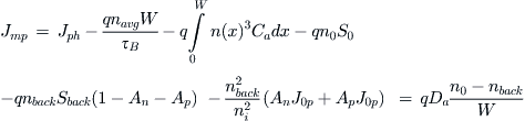
4 Modelling of Back-Contact Solar Cells
The simplest way to model IBC solar cells is to consider it as a back-surface–illuminated p–n junction solar cell. As an example, we can use the integral approach as proposed by R.M. Swanson [9,10,12]. For a precise simulation of an IBC or PC solar cell, we refer the reader to the model developed in these papers that includes quasi-3D effects close to the back contacts. In the following, we give a simple formulation.
The current, I, at the terminals of a solar cell can be written in the form
![]() (4)
(4)
where Iph, is the photogenerated current (the maximum photogenerated current within the silicon material with a defined thickness, including reflection losses and light trapping), Ib,rec is the sum of all the bulk recombination currents (including SRH and Auger recombination), Is,rec is the sum of all the surface recombination currents (including front side, back, and edge surface recombination), and Iem,rec is the sum of all the emitter recombination currents (including back emitters, the front TJ or FSF emitter if it exists, and also recombination at the contacts). The recombination currents increase as the carrier concentration increases and therefore increase as the terminal voltage increases. Eventually, at the open-circuit condition, the sum of all the recombination currents will be equal to the photocurrent, Iph, and the terminal current will be equal to zero. Therefore, at Voc:
![]() (4)
(4)
Calculating the different components of the recombination current is the most interesting and most powerful approach to simulate, optimise, or analyse the performance of solar cells. In particular, it provides a good method for a power-loss analysis. Table 1 gives a summary of the different relevant recombination mechanisms in silicon, their controlling parameters, typical values in high-efficiency one-sun or concentrator silicon solar cells, and the corresponding recombination currents.
TABLE 1 Recombination Mechanisms and the Corresponding Recombination Currents in n-Type Silicon Solar Cells Under High-Level Injection (HLI) and Low-Level Injection (LLI)

The ambipolar Auger coefficient value is from Sinton [11,12]. In this chapter, τB represents the bulk lifetime, either τn or τp in LLI. When we are considering HLI, we have assumed that τB = τp+τn, where τn and τp are the electron and the hole lifetimes.
If an IBC solar cell is to be modelled in a simple manner as a back-surface–illuminated conventional solar cell, one has to realise the following:
• In most of the device, the electron and holes are flowing in the same direction, from the front side of the cell toward the back, where the collecting n-type and p-type junctions are.
• When the cell is under HLI and the electrical neutrality in the bulk is to be maintained, the electron and hole concentrations are equal throughout the device and are flowing with the same ambipolar diffusion constant, Da = 2DnDp/(Dn+Dp), where Dn and Dp are the electron and hole diffusion constants.
• In most of the device, from the front side to very close to the emitter area where 3D current flow starts to appear, the current flow is almost unidirectional, perpendicular to the surface:
• in low-level injection (LLI) and for an n-type substrate,
![]() (6)
(6)
![]() (7)
(7)
where Jn and Jp are the electron and hole current densities, and therefore the total current along the wafer JT is negligible far away from the collecting junctions:
![]() (8)
(8)
Since carrier concentration at the cell back is determined by the terminal voltage of the solar cell:
![]() (9)
(9)
![]() (10)
(10)
we can use Equation (4) and the expression of recombination currents in Table 1 to calculate the cell current at any bias voltage. As a simple example, we can take a high-efficiency IBC or PC solar cell under HLI with long carrier lifetime (τB = τn+τp ![]() W2/Da, where W is the thickness of the cell) and low surface recombination velocity (S0
W2/Da, where W is the thickness of the cell) and low surface recombination velocity (S0 ![]() Da/W, where So is the real or effective surface recombination velocity at the front surface).
Da/W, where So is the real or effective surface recombination velocity at the front surface).
In short-circuit condition, we can consider that, in the first approximation,
• the emitter and surface recombination currents at the back of the cell can be neglected, as well as Auger recombination; and
• the electron and hole concentrations linearly decrease from front to back.
Equation (4) then becomes
![]() (11)
(11)
where Jsc is the short-circuit current density, n0 is the front-surface electron concentration, and currents were replaced by current densities in view of the effectively planar geometry of the cell as a result of the perpendicular direction of the current. A few iterations are necessary to determine the short-circuit current and the front-surface carrier concentration.
It becomes immediately apparent that if the thickness of the cell, W, increases, the front-surface carrier concentration, n0, increases, which, in turn, results in increased bulk and front-surface recombination currents.
In open-circuit condition, we can consider that the electron and hole concentrations are constant throughout the device. The open-circuit voltage is given by
![]() (12)
(12)
after solving the following equation:
![]() (13)
(13)
where J0n and J0p are the saturation current densities at the n and p junctions; An and Ap are the n-type and p-type emitter coverage fractions, respectively; and Sback is the surface recombination velocity at the back of the cell.
The maximum power point and efficiency of the solar cell can be determined the same way, considering that the back-carrier concentration is given by Equation (10) and that the carrier concentration is still linearly distributed from front to back. Equation (4) becomes
 (14)
(14)
where navg = (n0 + nback)/2 is the average carrier concentration and
![]() (15)
(15)
Several iterations are necessary to reach the solution.
This is a very simple way to analyse the IBC or PC solar cells. It allows for a quick determination of the carrier concentration in the device and an analysis of the different recombination mechanisms. Note that Equation (1) or (2) must be used for the front-side recombination current expression in FSF or TJ solar cells. For a more precise modelling, including quasi-3D effects at the back surface of the solar cell, the reader is referred to the Swanson model [9,10].
IBC solar cells for one-sun applications can be easily modelled using the LLI Equations (1), (6), (9) and the LLI recombination currents in Table 1. However, one needs to remember that, in most high-efficiency solar cells, the device is in LLI at short-circuit condition but actually in HLI at open-circuit condition. At the maximum power point, the device is often at the limit of HLI.
5 Perimeter and Edge Recombination
So far, we have not considered the edge recombination. It has been recently demonstrated that, in most high-efficiency silicon solar cells, one of the most important recombination mechanisms is a recombination current at the unpassivated surface at the edge of the silicon die [13]. Two cases need to be considered here:
• aperture-illuminated solar cells (e.g., cells for Fresnel lens modules, Figure 2), and
• totally illuminated solar cells (e.g., cells for one-sun application or CPV cells for dense-array receivers, dish, and thermophotovoltaic [TPV] applications, Figure 3).
In order to reduce the edge recombination, the aperture-illuminated IBC solar cells must have its active area as far as possible from the edge of the silicon die—in theory, at a distance of least three times the ambipolar diffusion length at the considered carrier concentration. In practice, economical considerations prevent manufacturers from increasing this distance too much, so a typical distance between the edge of the silicon die and the nearest emitter at the back of the cell is about 500 μm. For totally illuminated solar cells, there is an optimal distance that can be calculated as explained in [13]. The width of the border region is optimal when the illuminated border region generates just enough current to supply the recombination current at the edge of the silicon die. A wider or narrower border region than the optimal width would result in a lower efficiency. If d is the width of the border region, P the cell perimeter, and p the average carrier density at the middle of the cell, at the maximum power point (Vm, Im) and at the considered concentration ratio, the current generated by the border region is
![]() (16)
(16)
and the edge recombination current is
![]() (17)
(17)
The border width is optimal when
![]() (18)
(18)
and
![]() (19)
(19)
In LLI, use Dp instead of Da in Equations (17) and (19).
For a fixed geometry and cell thickness, the carrier concentration and short-circuit current are more or less proportional to the concentration ratio. Therefore, the optimal border width is generally independent of the concentration ratio. However, since the average carrier concentration increases with the thickness of the cell, the optimal border width is roughly proportional to the thickness of the cell. For a typical IBC solar cell for dense-array application at ×400 and with a thickness of 100 μm (n ≈ 1017 cm−3), the optimal border width is about 135 μm.
Equation (19) is valid if the edge is unpassivated (assuming infinite recombination velocity) such as in silicon solar cells diced with a dicing saw. New techniques to passivate the edges of solar cells are needed, but so far there has been no satisfactory development in low-temperature passivation of silicon surfaces after dicing.
6 Manufacturing Process for Back-Contact Solar Cells
The typical six-mask process flow to manufacture IBC solar cells for CPV application and with a double-level metallisation scheme is presented in Figure 8, although actual processes may significantly differ in practice. A typical low-cost process for one-sun IBC solar cells requires only three lithography steps: junction, contact, and metal [33,36]. Developing a low-cost lithography technology has been the key driver for making commercial flat-plate PV modules with IBC cells a reality. On the other hand, when very high efficiencies are desired, additional photolithography steps may be required for

FIGURE 8 Process flow of manufacturing IBC solar cells.
7 Stability of Back-Contact Cells
In the same way as many other high-efficiency silicon solar cells, the IBC cells are subject to efficiency degradation. If FZ wafers are used, the degradation is limited to the silicon–silicon dioxide interface [1,14–16]. The degradation of the interface could be due to the loss of hydrogen atoms passivating the dangling bonds at the silicon–silicon dioxide interface or the creation of new interface states. The degradation of the interface is manifested by:
• an increase of the surface recombination velocity, which, in turn, results in a reduction of the short-circuit current over the entire range of concentration ratio, or
• an increase of the front emitter current J0 that results in an increase of the sublinearity (the cell responsivity decreases as the concentration ratio increases) if the front surface is lightly doped or inverted due to charges in the dielectric layer.
Both mechanisms will result in a significant decrease in efficiency. The degradation has been observed so far due to the following individual or combined conditions:
• UV light, which creates hot electrons that can overcome the potential barrier at the silicon–silicon dioxide interface and create new interface states;
• elevated temperature (>100°C), which allows hydrogen atoms to escape from the interface; and
It is also assumed that the following conditions enhance the degradation:
• highly concentrated sunlight, which creates a large concentration of carriers at the surface of the solar cell;
• the presence of moisture; and
• the presence of atomic hydrogen, which could break an existing Si–H bond to form a hydrogen molecule H2.
There is still much research to be done to understand the degradation mechanisms and to find a solution to this issue.
The easiest way to prevent the strong influence of the degradation of the surface recombination velocity to solar cell efficiency is to isolate the surface from the rest of the cell with FSF or a floating tandem junction. Unfortunately, although it makes the cell more stable, the front-side emitter has a significant impact on the sublinearity of the solar cell [1,15], which makes this solution undesired for concentration applications. In any case, the front emitter must be lightly doped in such way that the front-emitter saturation current, J0+, is kept as low as possible. Indeed, we can see from Equation (2) that the greater the front emitter J0+, the more significant the sublinearity of the solar cell will be.
There are other ways to ensure stability of the IBC solar cells:
• During the solar cell fabrication, it is very important that the front passivating oxide layer is grown with the smallest interface state density. 1,1,1-trichloroethane (TCA), dichloroethane (DCA), trichloroethylene (TCE), or HCl oxide growth, as well as an aluminium anneal, should be avoided for the final oxidation as they have been recognised as giving very unstable Si–SiO2 interfaces [16,17].
• UV light with wavelengths below 400 nm should be filtered from the solar spectrum, either at the solar cell level or at the concentrator module level. For example, the ARC can include a UV filter such as TiO2 or a very thin polysilicon layer [14,16].
• The front surface of the solar cell should be coated with a thin layer of silicon nitride (as part of the ARC) or another material, hopefully compatible with the ARC, to form a great hydrogen and moisture diffusion barrier (for example, a very thin amorphous silicon or polysilicon layer) [16].
Another mechanism of degradation has been observed in IBC solar cells [38]. Since the front surface of the cells is undoped (in the case of PC cells, for example) or very lightly doped (in the case of FSF or TJ cells), it can easily be brought into depletion by electric charges. When the front surface is depleted, the front-surface recombination current significantly increases and the efficiency decreases. The electric charges can be easily reversed in the factory and the original module performance can be reestablished. As an example of solution to this problem, the positive DC leg of an array of flat-plate PV modules containing n-type IBC or FSF solar cells should be earthed in order to prevent the front surface from being negatively charged and to prevent the front surface of the cells from being depleted. With the positive DC leg being earthed, the front surface of the cells stay positively charged and stay in accumulation. For the same reason, floating PV array schemes and transformerless inverters are not to be used with PV systems using IBC cells.
The two mechanisms of degradation described above are not exclusive to IBC cells. They are observed in any solar cell presenting a lightly doped front surface; the methods of prevention are identical for all cells.
8 Toward 30% Efficiency Silicon Cells
In 1985, Gray and Schwartz presented a paper titled ‘Why Don’t We Have a 30% Efficient Silicon Solar Cell?’ [18]. At that time, the highest reported efficiency for silicon solar cell was 22% under concentrated sunlight. In that paper, the authors concluded that 30% efficiency would be attainable with a silicon solar cell if
• good light trapping was developed that did not degrade the open-circuit voltage of the solar cell,
• the contact and grid series resistance could be reduced enough to allow for a high concentration ratio,
• the current crowding effects are reduced by a judicious design, and
• a novel heterojunction or hetero-interface contact with small contact resistance and low emitter saturation current was developed.
A few years later, the first three steps to attain the 30% efficiency target had been addressed and resolved: the PC solar cell with a thin substrate and long carrier lifetime, with a textured and passivated front surface, proved to be the best design for high-efficiency concentrator solar cell [19,20]. In 1989, the highest reported efficiency for silicon PC solar cell was 28.3% [21]. The same year, Swanson responded to Gray’s paper in a publication titled “Why We Will Have a 30% Efficient Silicon Solar Cell” [22] in which he demonstrated that all the pieces were in place to fabricate a 30% efficient silicon solar cell. The last milestone to reach the 30% breakthrough—namely, the development of polysilicon emitters with a low contact resistance and low emitter saturation currents—had just been demonstrated at Stanford [23,24]. Swanson announced, “Within one year, cells will be reported with efficiency in excess of 30%” [22].
It is believed that 30% efficient silicon CPV solar cells are possible in a manufacturing environment. In order to achieve this goal, polysilicon or heterojunction emitter technology needs to be implemented, along with several other improvements to the existing technology (thinner cells, improved light trapping, and reduced dimension geometries).
9 How to Improve the Efficiency of Back-Contact Solar Cells
Campbell and Green [25] discussed the efficiency limit of silicon solar cells under concentrated sunlight. They showed that the limit of efficiency for a silicon cell is between 30% and 35%. These very high efficiencies have never been demonstrated so far with a single-junction silicon solar cell. Commercially available PC concentrator cells have efficiencies around 26.5%. In order to reach such high efficiencies, the recombination mechanisms such as trap-assisted SRH recombination, in the bulk or at the surface, and emitter recombination must be negligible compared to Auger recombination. The Auger recombination is intrinsic to the material and, for example, cannot be improved by using a purer starting material or a cleaner fabrication process. Therefore, the only way to reduce the Auger recombination rate inside the cell is to reduce its thickness. However, using a very thin silicon solar cell requires the use of a very effective scheme for light trapping. For example, Campbell and Green [25] suggest that the optimum cell would be less than 1 μm thick and could reach 36–37% under concentration.
By comparison, the recombination in the PC solar cell at ×250 (25 W/cm2) is almost equally dominated by emitter (40%) and Auger (40%) recombination. The surface and bulk SRH recombination represents less than 20% of the overall recombination rate. In the PC design, the emitter coverage fraction has already been reduced to the minimum technologically acceptable, and the only way to further reduce the emitter recombination rate is to reduce the emitter saturation current density J0. Therefore, in order to reach 30% or greater efficiency, the following strategy needs to be used:
1. Reduce the emitter recombination by reducing the emitter saturation current density from 2×10⁻¹³ to 5×10⁻¹⁴ A/cm2. Polysilicon heterojunction emitters with less than 5×10⁻¹⁴ A/cm2 as saturation current density have already been demonstrated [23,24].
2. Demonstrate low contact resistance between the bulk and the emitters. A desired value for the contact resistance between bulk and emitter is less than 10−5 Ω cm2.
3. Reduce the cell thickness in order to reduce the Auger recombination rate. For a practical concentrator for which the angle of incidence of the light to the cell is between 0 and 30 degrees, the optimal thickness is about 30 μm [25]. This is very difficult to achieve in a manufacturing environment. Manufacturing techniques, such as local thinning, need to be implemented.
4. Improve light trapping by designing new textured surfaces on both sides of the cell.
5. Reduce the unit cell geometry down to a dimension equal to or smaller than the thickness of the cell.
6. Reduce the external series resistance (metal and interconnect).
9.1 Reduce Emitter Saturation Current Density
The saturation current density of an emitter J0 represents the sum of all the recombination mechanisms inside the emitter. It includes the SRH, surface, contact, and Auger recombination mechanisms, as well as heavy doping effects such as band-gap narrowing. The best diffused emitter J0 that can be achieved is around 2×10⁻¹⁴ A/cm2. However, such an emitter is very transparent, which means that if a metal contacts it, its saturation current density dramatically increases about 100-fold. For contacting PC solar cell, the emitter must be opaque and the best saturation current density of such emitter is around 2×10⁻¹³ A/cm2.
An ideal emitter for silicon should be transparent to majority carriers and a mirror for minority carriers. Therefore, it should have a wide band gap such that an additional potential barrier will appear in the minority band when it is doped (see Figure 9). Although there are many semiconductors with a larger band gap than silicon, so far none of the large band-gap materials have proved to be ideal for contacting silicon. Indeed, the potential barrier at the emitter heterojunction blocks the minority carriers; they still can recombine at the heterojunction interface due to the presence of interface traps.
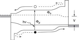
FIGURE 9 Band diagram of a p–i–n solar cell with heterojunction emitters.
There are only two materials that were reported to emitters with low J0: polysilicon emitters and semi-insulating polysilicon (SIPOS) emitters, both used with an interfacial thin oxide layer [23,24,26,27]. However, some very promising results have recently been reported on nonconcentrator solar cells with amorphous silicon emitters [28] that do not require an interfacial thin oxide to block the minority carriers.
9.2 Demonstrate Low-Contact Resistance
The growth of a thin (10 Å to 20 Å) interfacial layer of silicon dioxide is critical to obtain low emitter saturation current density with polysilicon. However, in order to achieve a low contact resistance, it is necessary to anneal the polysilicon emitter to break up the oxide layer on about 1% of the contact area [23]. The trade-off between J0 and a high contact resistance is highly dependent on the oxide thickness and the anneal (or breakup) step.
9.3 Reduce the Cell Thickness
Once the emitter recombination mechanism has been reduced, it is possible to reduce the Auger recombination rate by using a thinner substrate for the solar cell. Solar cells made on 100-μm-thick wafers can be manufactured in large volumes, but thinner cells present a real challenge for manufacturing. Since both sides of the cells must be processed for texturing, passivation, and antireflection coating, the thinning of the wafers cannot just be done by lapping the wafers at the end of the process. Solar cells of 30–80-μm thickness must be fabricated on locally thinned substrates.
9.4 Improve Light Trapping
When very thin silicon solar cells are designed, the light-trapping property of the cells becomes a significant factor for the efficiency. Currently available cells have only one-side texturisation. Unfortunately, this is not enough for cells thinner than 100 μm. In this case, a double side texturisation or perpendicular grooving must be designed in order to ensure good light trapping. In current PC solar cells, the analysis of the internal quantum efficiency near the edge of the band gap shows that the effective number of passes for long-wavelength light is greater than 30 [1]. The light trapping can be improved with double side texture, perpendicular slats, or parquet grooves in order to attain as many as 50 passes of the light.
9.5 Shrink Geometries
Currently available PC solar cells have a significant current crowding loss and large internal series resistance accounting for about 0.002 Ω cm2, which represents about 3% power loss at 25 W/cm2 or 250×. The unit cell dimension should be reduced from the current 140 μm to 40 μm and to 25 μm if possible. The metallisation and intermetal dielectric technology usually prevents the shrinking of the unit cell. In order to be able to shrink the unit-cell dimension to 40 μm or even 25 μm, a state-of-the-art plasma etching process for the metal, as well as a plasma-enhanced chemical vapour deposition (PECVD), SiO2-based dielectric as intermetal dielectric layer must be adopted.
9.6 Reduce Series Resistance
Shrinking the geometries of the unit cell in order to reduce the internal series resistance may have a negative effect on the external series resistance. This problem is due to the fact that, if the gap between metal lines is kept constant, the metal coverage fraction decreases with decreasing the dimensions of the unit cell. A new metallisation design, similar to what has been proposed in previous papers [4,5], must be implemented in order to reduce the series resistance. As in step 9.5, the new metal design requires a plasma etching process for metal and a SiO2-based dielectric layer. The target is to reduce the total series resistance to less than 0.001 Ω cm2, or about a 2.5% power loss at ×500 concentration.
TABLE 2 Strategy for 30% Efficient PC Silicon Solar Cells for CPV Applications
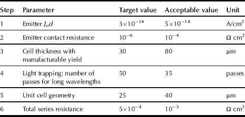
9.7 Target Performance
Table 3 shows the target performance of a 30% efficient silicon solar cell compared to the commercially available point-contact solar cells. Figure 10 shows the improvement in efficiency based on the above strategy. Of course, the full benefit of the polysilicon emitter with low J0 is observed when all the other improvements (thinner cells, improved light trapping, and shrunk geometries) are in place.
TABLE 3 Comparison of Performance of a Commercial PC Solar Cell (HECO335 from SunPower Corporation) Cell with the Projected New High-Performance Cell at ×100 and ×275 (AM1.5D, 10 and 27.5 W/cm2, τc = 25°C). The values at ×275 Concentration are in Parentheses


FIGURE 10 Efficiency (AMI. 51, 25°C) of the point-contact silicon solar cell versus incident power density after each step of this strategy.
10 Conclusions
Interdigitated-back-contact and point-contact silicon solar cells have been demonstrated to be the most efficient and most suitable silicon solar cells for one-sun and high-concentration applications. Commercially available PC solar cells have demonstrated efficiencies up to 27.6% (at 9.2 W/cm2, AM1.5D, 25°C) in large-volume production. The best large-area IBC silicon solar cell for one-sun applications has an efficiency of 24.2%. Commercially available large flat-plate PV modules with IBC silicon solar cells have demonstrated efficiencies greater than 21%. This chapter has described the structure of IBC, FSF, TJ, and PC cells, as well as the process to fabricate them. A simple model for the simulation, optimisation, and analysis of the different recombination mechanisms in one-sun and concentrator IBC cells has been presented. Finally, we have presented a plan for the development of 30% efficiency concentrator PC solar cells.
Acknowledgements
The author would like to thank A. Terao and S. Daroczi of SunPower Corporation and J. Lasich of Solar Systems Pty Ltd for supplying pictures of the point-contact solar cells and the concentrator PV systems.
References
1. Verlinden PJ, Swanson RM, Crane RA, Wickham K, Perkins J. A 26.8% Efficient concentrator, point-contact solar cell. Nice: Proceedings of the 13th European Photovoltaic Solar Energy Conference; 1995; pp. 1582–1585.
2. Sinton RA, Swanson RM. Development efforts on silicon solar cells. Final Report Palo Alto, CA: Electric Power Research Institute; February 1992; pp. 2–44.
3. Swanson RM, Sinton RA, Midkiff N, Kane DE. Simplified designs for high- efficiency concentrator solar cells. Albuquerque, NM: Sandia Report, SAND88–0522, Sandia National Laboratories; July 1988;.
4. Verlinden PJ, Swanson RM, Sinton RA, Kane DE. Multilevel metallization for large area point-contact solar cells. Las Vegas: Proceedings of the 20th IEEE Photovoltaic Specialists Conference; 1988; pp. 532–537.
5. Verlinden PJ, Sinton RA, Swanson RM. High-efficiency large-area back contact concentrator solar cells with a multilevel interconnection. Int Journal of Solar Energy. 1988;6:347–365.
6. Verlinden PJ, Terao A, Smith DD, et al. will we have a 20%-efficient (ptc) photovoltaic system?. Munich: Proceedings of the 17th European Photovoltaic Solar Energy Conference; 2001; pp. 385–390.
7. Schwartz RJ, Lammert MD. IEEE International Electron Devices Meeting. Washington DC 1975;:350–351.
8. Lammert MD, Schwartz RJ. IEEE Trans Electron Devices ED-24(4) 1977;:337–342.
9. Swanson RM. Point contact silicon solar cells, theory and modeling, Proceedings of the 18th IEEE Photovoltaic Specialist Conference. Las Vegas 1985; pp. 604–610.
10. Swanson RM. Point contact solar cells, modeling and experiment. Solar Cells. 1988;Vol. 7(1):85–118.
11. Sinton RA. Device Physics and Characterization of Silicon Point-Contact Solar Cells. Stanford, CA: Stanford University; 1987; Ph.D. Thesis.
12. Sinton RA, Swanson RM. Recombination in highly injected silicon. IEEE Trans Electron Devices ED-34(6) 1987;1380.
13. Sinton RA, Verlinden PJ, Swanson RM, Crane RA, Wickham K, Perkins J. Improvements in silicon backside-contact solar cells for high-value one-sun applications. Nice: Proceedings of the 13th European Photovoltaic Solar Energy Conference; 1995; pp. 1586–1589.
14. Gruenbaum PE, Gan JY, King RR, Swanson RM. Stable passivations for high- efficiency silicon solar cells. Kissimmee: Proceedings of the 21st IEEE Photovoltaic Specialists Conference; 1990; pp. 317–322.
15. Verlinden PJ, Swanson RM, Sinton RA, et al. High-efficiency point-contact silicon solar cells for fresnel lens concentrator modules. Louisville: Proceedings of the 23rd IEEE Photovoltaic Specialists Conference; 1993; pp. 58–64.
16. Gruenbaum PE. Photoinjected Hot-Electron Damage at the Silicon/Silicon Dioxide Interface in Point-Contact Solar Cells. Stanford: Stanford University; 1990.
17. Cudzinovic M, Pass T, Terao A, Verlinden PJ, Swanson RM. Degradation of surface quality due to anti-reflection coating deposition on silicon solar cells, Proceedings of the 28th IEEE Photovoltaic Specialists Conference. Anchorage 2000; pp. 295–298.
18. Gray JL, Schwartz RJ. Why don’t we have a 30% efficient silicon solar cell?. Las Vegas: Proceedings of the 18th IEEE Photovoltaic Specialists Conference; 1985; pp. 568–572.
19. Verlinden P, Van de Wiele F, Stehelin G, David JP. An interdigitated back contact solar cell with high efficiency under concentrated sunlight. Seville: Proceedings of the 7th European Photovoltaic Solar Energy Conference; 1986; pp. 885–889.
20. Sinton RA, et al. 27.5 Percent silicon concentrator solar cells. IEEE Electron Device Letters EDL-7(10) 1986;567–569.
21. Sinton RA, Swanson RM. An optimization study of si point-contact concentrator solar cells. New Orleans: Proceedings of the 19th IEEE Photovoltaic Specialists Conference; 1987; pp. 1201–1208.
22. Swanson RM. Why we will have a 30% efficient silicon solar cell. Sydney: Proceedings of the 4th International Photovoltaic Science and Engineering Conference; 1989; pp. 573–580.
23. Gan JY. Polysilicon Emitters for Silicon Concentrator Solar Cells. Stanford: Stanford University; 1990; Ph.D. Thesis.
24. Gan JY, Swanson RM. Polysilicon emitters for silicon concentrator solar cells. Kissimmee: Proceedings of the 21st IEEE Photovoltaic Specialists Conference; 1990; pp. 245–250.
25. Campbell P, Green M. The limiting efficiency of silicon solar cells under concentrated sunlight. IEEE Trans Electron Devices ED-33(2) 1986;234–239.
26. Christel LA. Polysilicon-contacted P+ emitter for silicon solar cell applications. Sandia National Laboratories Report SAND87–7021 1987.
27. Kwark YH, Swanson RM. SIPOS heterojunction contacts to silicon. Sandia National Laboratories Report SAND85–7022 1985.
28. Sakata H, Kawamoto K, Taguchi M, et al. 20.1% Highest efficiency large area (101cm2) HIT cell. Anchorage: Proceedings of the 28th IEEE Photovoltaic Specialists Conference; 2000; pp. 7–12.
29. Verlinden PJ, Swanson RM, Crane RA. 7000 High-efficiency cells for a dream. Prog Photovolt – Res Appl. 1994;2:143–152.
30. Verlinden PJ, Swanson RM, Crane RA. High efficiency silicon point-contact solar cells for concentrator and high-value one-sun applications. Amsterdam: Proceedings of the 12th EC Photovoltaic Solar Energy Conference; 1994; pp. 1477–1480.
31. Verlinden PJ, Crane RA, Swanson RM, et al. A 21.6% Efficient photovoltaic module with backside contact silicon solar cells. Amsterdam: Proceedings of the 12th EC Photovoltaic Solar Energy Conference; 1994; pp. 1304–1307.
32. Zhou CZ, Verlinden PJ, Crane RA, Swanson RM. 21.9% Efficient silicon bifacial solar cells. Anaheim: Proceedings of the 26th IEEE Photovoltaic Specialists Conference; 1997; pp. 287–290.
33. Mulligan WP, et al. Manufacture of solar cells with 21% efficiency. Proceedings of the 19th European Photovoltaic Solar Energy Conference 2004; p. 387.
34. De Ceuster D, Cousins PJ, Rose D, Vicente D, Tipones P, Mulligan W. Low cost high volume production of .22% efficiency solar cells. Proceedings of the 22nd European Photovoltaic Solar Energy Conference 2007; pp. 816–819.
35. Cousins PJ, Smith DD, Luan H-C, et al. Generation 3: Improved performance at lower cost. Honolulu: Proceedings of the 35th IEEE Photovoltaic Specialists Conference; 2010; pp. 275–278.
36. Sinton RA, Swanson RM. Simplified backside-contact solar cells. IEEE Trans Electron Dev. 1990;37(2):348–352.
37. Slade A, Garboushian V. 27.6% efficient silicon concentrator cell for mass production. Shanghai: Technical Digest of 15th International Photovoltaic Science and Engineering Conference; October 2005; p. 701.
38. SunPower Corporation Press Release. August 22, 2005; In: http://investors.sunpowercorp.com/releasedetail.cfm?ReleaseID5179402/; August 22, 2005.