5.10. Direct Port-Connected Topologies
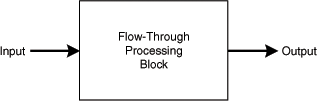
Buses cannot cleanly support the type of flow-through processing systems commonly implemented using custom-designed logic, shown in Figure 5.11, because buses only permit one I/O transaction at a time. Flow-through processing blocks implemented in custom hardware usually perform input and output operations simultaneously in a pipelined fashion to improve throughput.
Figure 5.11. A flow-through processing block takes in data, processes it, and outputs the result. All three operations can occur simultaneously. Custom-designed hardware blocks often work in this manner but most processors with their bus-based I/O must emulate flow-through operations because their buses only permit one I/O transaction at a time.
The ability to perform simultaneous input and output operations along with internal data computations is one of the key performance advantages of flow-through processing. Many system designs that construct dataflow architectures from multiple processors—architectures often employed in signal- and image-processing applications for example—can benefit from the additional I/O performance provided by true flow-through processing.
Processor cores that perform all I/O transactions over buses can only emulate the operation of flow-through functional units because they can only operate one of their buses at a time and a bus can only conduct one transaction (input or output) at a time. However, using bus-based processors to emulate flow-through functional units has become so ingrained into the modern system-design lexicon that the overhead of using inherently half-duplex buses to mimic flow-through operation has become all but invisible.
Ports and queue interfaces on Xtensa and Diamond processor cores directly support flow-through processing. Figure 5.12 shows how ports can tie an Xtensa or Diamond processor core directly to a custom-designed or pre-existing logic block and Figure 5.13 shows how the RTL block fits into the processor’s pipeline stages.
Figure 5.12. Ports allow an Xtensa or Diamond processor core to directly interact with a custom-designed or preexisting logic block.

Figure 5.13. One instruction drives the processor’s output-port pins that control the external RTL block and another instruction reads the result returned from the RTL block on the processor’s input-port pins.

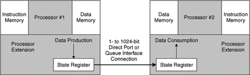
Ports and queue interfaces can also directly tie two processors together, as shown in Figure 5.14. Because these connections exploit the descriptive abilities of TIE, the inter-processor connections are not limited to the widths of their buses. Each port or queue connection can be as wide as 1024 bits and each processor can have hundreds of such connections.
Figure 5.14. Ports and queue interfaces can directly connect two Xtensa or Diamond processor cores.
If Xtensa processors were individual chips used on circuit boards, the high I/O pin counts resulting from heavy use of TIE ports and queue interfaces would be unthinkable or merely economically unfeasible. However, Xtensa processors are IP cores implemented in nanometer-fabrication technology so the notion of hundreds of wires connecting two adjacent processors is no longer unthinkable or even unreasonable if you clear your mind of the old-fashioned design constraints previously placed on system architectures that are no longer applicable in the 21st century.
In fact, such high pin counts may actually be very desirable because they potentially reduce processor clock rate. If hundreds of bits are transferred between processors or between a processor and a hardware block during each clock period, there’s much less incentive to quest for high I/O bandwidth by running the processor at higher clock rates. System architectures that employ wide I/O buses between adjacent processors and other logic blocks may become highly desirable for these reasons.
However, connecting widely separated processors and logic blocks with wide buses on an SOC is highly undesirable because stringing wide buses across long distances on a chip can create severe routing congestion and high capacitive loading, which will both degrade signal integrity. Consequently, the use of wide I/O buses for on-chip inter-processor communications must be supported with good chip floorplanning and block placement to minimize the length of the bus runs.