
2
FO‐WLP Market and Technology Trends
E. Jan Vardaman
TechSearch International, Inc., Austin, TX, USA
2.1 Introduction
The quest for thin, low profile packaging solutions for mobile devices and cost reduction with improved performance continues to drive the development of new packages. The development of the fan‐out wafer‐level package (FO‐WLP) is the latest industry trend. There are an increasing number of suppliers for FO‐WLP and a growing number of applications. This chapter examines the market trends and drivers for package adoption and the technology trends for FO‐WLP.
2.2 FO‐WLP: A Disruptive Technology
An FO‐WLP is a substrate‐less package that typically uses a carrier and mold compound to create a format on which single or multiple dies are placed and a redistribution layer (RDL) is used to “fan out” the inputs and outputs (I/Os) to create a package. When Infineon developed its FO‐WLP, the embedded wafer‐level ball grid array (eWLB), one of the drivers was to reduce package cost by removing costly parts of the package including the substrate and the flip‐chip bump. The absence of a substrate makes FO‐WLP a disruptive technology. Thin film metallization is used for interconnect instead of bumps or wires. Infineon’s FO‐WLP has the active side of the die placed facedown in the process and so is often referred to as a face‐down FO‐WLP. In the case of a face‐up process, the die has a thick Cu post. Figure 2.1 shows a face‐up and a face‐down option.

Figure 2.1 (a) Active die face‐down FO‐WLP die placement. (b) Active die face‐up FO‐WLP die placement.
Source: Courtesy of ASE.
The use of a thin film process instead of a laminate substrate makes it possible to achieve much finer feature sizes. Laminate substrates are in high volume production with 15 μm lines and spaces, with some leading‐edge production of 10 μm lines and 9 μm spaces. Achieving higher routing densities such as less than 5 μm lines and spaces may be costly.
2.3 Embedded Die Packaging
FO‐WLP is a form of embedded die. An embedded component is defined as an active or passive device that is placed or formed on an inner layer of an organic circuit board, module, or chip package, such that it is buried inside the completed structure, rather than on the top or bottom surface. Adoption of embedded active components is being driven by demands for smaller form factors and improved performance. Some companies embed active components on an inner layer of the IC package or module substrate with a lamination process. Other companies embed RF components such as Bluetooth devices in the product board with a lamination process. The embedded component can take the form of bare die or a wafer‐level package.
One of the early examples of embedded components is General Electric (GE) with its chips first buildup technology. The GE technology was originally targeted at applications such as high‐end military and space applications including complex multiprocessor modules, memory modules, 3D structures, and CSPs. The key feature of this technology is the direct metallization connection between the chip and the package, accomplished through laser drilling of vias directly through the polyimide film to the chip I/O pads followed by sputtering of a seed layer metal and semi‐additive buildup plating of copper conductors [1]. GE subsequently acquired the assets and technology from Imbera Electronics Oy and has developed a process to embed die in flex circuit for power device applications. The technology has been licensed to Shinko Electric and Flexceed in Japan.
Austria Technologie & Systemtechnik (AT&S) is located in Austria and started building and testing embedded component packaging (ECP®) technology in 2009. This technology is used for power modules and other applications. Applications at AT&S include automotive and mobile products. AT&S provides the embedding for Texas Instrument’s (TI) MicroSiP TPS8267, a 650 mA DC/DC converter. Products use the ECP chip‐first process flow.
TDK Corporation developed the embedded die solution called semiconductor embedded in substrate (SESUB®). The technology is in production for power management integrated circuits (PMICs). Battery charger products have also been demonstrated with the technology. TDK also introduced an ultracompact Bluetooth low‐energy module designed for Bluetooth 4.0 low energy specifications targeted for wearable electronics products. The package is 4.6 mm × 5.6 mm × 1.0 mm. The Bluetooth IC die is embedded into the thin substrate; the peripheral circuitry including a quartz resonator, bandpass filter, and capacitors is integrated on the top. The module is 65% smaller than the alternative with individual discrete components.
Casio Micronics and CMK Corporation have developed an embedded wafer‐level packaging (EWLP) technology. Target applications include stacked memory modules, memory cards, Bluetooth™ modules, and camera modules. Casio shipped several products using the technology. The main product was a mobile TV tuner.
DNP is located in Japan and began volume production of embedded passive devices (EPD) in 2006 and embedded active devices (EAD) in 2007. The devices are used in a range of configurations from packages to PCBs, including package‐on‐package (PoP) substrates, camera modules, and motherboards for mobile phone applications.
Fujikura developed a multilayer flex circuit fabrication process that allowed WLPs to be embedded in the flexible substrate layers. This freed the surface space for other components to be mounted, and the module can be reduced in size. Fujikura shipped samples designed for camera and Bluetooth modules used in mobile phones.
Driven by the need for miniaturization in mobile applications, DNP developed a B2 it PCB with EPD and EAD. The use of embedded components offers a smaller area and improved electrical performance, and the technology was used to embed passive devices.
Samsung Electro‐Mechanics (SEMCO) developed the Smart Functional Circuits® for the integration of embedded actives and passives in PCBs and modules.
Taiyo Yuden has been manufacturing EAD substrates with its embedded organic module involved nanotechnology (EOMIN®) process since 2006. Most of the EAD are power management die, signal control die, and sensors. Applications include power management, signal processing, and sensing. Both active and passives can be embedded.
TI has been shipping its TPS8267x family of step‐down converters since 2010. These products are offered in an 8‐pin MicroSiP™ package. The active component is a switching regulator in TI’s PicoStar™ format that is embedded in an FR‐4 laminate‐type substrate. I/O capacitors and an inductor are mounted on the top surface of the substrate. This format enables a very low profile package.
3D Plus developed a stacked module technology that is also considered an embedded component package [2]. This module, called Walpack, was developed with partners STMicroelectronics, CEA‐Leti, Thales, Schlumberger, Cards/Axalto, Cybernetics, and IBS in a four‐year European program that operated from 2001 to 2004.
2.4 FO‐WLP Advantages
Advantages of FO‐WLP include:
- Form factor, low profile package, with small gap between the die and the package edge (≤50 μm).
- Support of increased I/O density while at the same time allowing the use of a WLP with die shrinks as companies move to advanced semiconductor technology nodes.
- Ability to support fine features roadmaps (≤10 μm lines and spaces).
- Split die or multi‐die packaging/system in package (SiP).
- Excellent electrical performance (low parasitic inductance, low insertion loss, and good signal integrity) because of the short signal path from the chip to package and to the board.
- Excellent thermal performance, especially when thermal balls are placed directly below the silicon die and the direct thermal path to the PCB due to the absence of a substrate.
- Sidewall protection on all slides resulting from the use of molding resin is advantageous when compared with fan‐in wafer‐level packaging (WLP), which has unprotected silicon sidewalls.
2.5 FO‐WLP Versions
Infineon developed the eWLB process in which dies are placed facedown on a metal carrier and molded into a reconstituted wafer. After removal from the carrier, a single or double RDL is used to fan out the I/Os. Solder balls are attached to the active side of the die, and then the reconstituted wafer is laser‐marked and singulated. The face‐down fan‐out process is illustrated in Figure 2.1.
ASE, NANIUM, and STATS ChipPAC licensed Infineon’s eWLB technology and have production lines. JCET, based in China, purchased STATS ChipPAC in 2015. Amkor purchased NANIUM in May 2017. SPIL is also establishing a production line with a chip‐first face‐down FO‐WLP process. SPIL’s encapsulated mold process uses a laser via formation and Cu post plating through package interconnection to fabricate a PoP. The die also has a copper pillar (this differs from the original eWLB process).
Freescale developed the redistributed chip package (RCP) process, which is a chip‐first face‐down process similar to eWLB in structure. Freescale Semiconductor (now NXP and soon to be part of Qualcomm) sold its 300 mm production equipment to nepes Corporation in 2009, but maintained a 200 mm pilot development line in Tempe, Arizona, until February of 2017. The nepes Corporation 300 mm production line is located in Korea. The process uses glass and ceramic carriers, and the devices are mounted facedown before molding (see Figure 2.2).
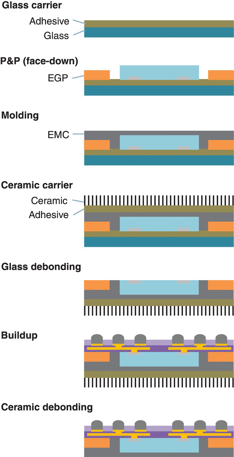
Figure 2.2 NXP’s RCP FO‐WLP process flow.
Source: Courtesy of NXP.
TSMC’s FO‐WLP version is called integrated fan‐out WLP (InFO‐WLP). In TSMC’s InFO process, a small Cu pillar interconnect is electroplated on the application processor. The die is placed faceup on the tape, followed by molding to create the reconstituted wafer. After grinding to reveal the top of the Cu pillar, the RDL is formed on the polished surface [3, 4]. A face‐up process is show in Figure 2.3.

Figure 2.3 Face‐up FO‐WLP process flow.
Deca Technologies, based in the Philippines, has also developed a face‐up structure. M‐Series is a fully molded FO‐WLP structure wherein mold compound protects the frontside of the die, in addition to providing fan‐out area at the periphery (see Figure 2.4). Covering the frontside of the die also prevents mold flash at the die edge boundary and die‐to‐mold compound coplanarity issues found in face‐down FO‐WLP solutions. These issues can cause issues for photolithography and solder bump reliability [5]. In the manufacturing process, copper pillar interconnects are fabricated on the native wafer, and the devices are singulated. The devices are attached faceup to a carrier with a temporary adhesive and overmolded. The temporary adhesive is removed, and the front of the panel is ground to reveal the copper studs.

Figure 2.4 Deca’s M‐Series® face‐up FO‐WLP process flow.
Source: Courtesy of Deca Technologies.
The next step uses Deca’s unique adaptive patterning process (see Figure 2.5). A high‐speed optical scanner measures the true position of the copper studs on each die on the reconstituted panel. A portion of the RDL design in close proximity to the die bond pads is recalculated using proprietary design software, generating a unique layout that accommodates die shift. Adaptive alignment shifts and rotates the first via and RDL to match the die location. A unique via and RDL pattern is dynamically applied to each panel using a mask‐less lithography system. The under‐bump metallization (UBM) pattern is kept fixed with respect to the package edge to maintain compliance with the package outline specifications [6].

Figure 2.5 Deca’s adaptive patterning process.
Source: Courtesy of Deca Technologies.
Amkor has introduced a chip‐last technology as an alternative to an FO‐WLP called silicon wafer integrated fan‐out technology (SWIFT®). It provides increased I/O and circuit density with a reduced footprint that can be used for single‐ or multi‐die applications. In the process, RDLs are formed on a carrier (see Figure 2.6). Flip‐chip bumped dies are attached to the high density structure with a minimum of 2 μm lines and spaces. Cu pillar pitch down to 30 μm is supported. A mold compound is used to encapsulate the structure and wafer backgrinding is used to thin the package [7]. Structures as thin as 500 μm with up to three RDLs can be created using the backgrinding process. The carrier can be inspected using automated optical inspection (AOI) to ensure it is a known good substrate and the die can be probed so that known good die (KGD) can be placed on good sites. With the Amkor process it is possible to create the tall Cu pillars for connection, or a through‐mold via (TMV) process with solder balls can be used.

Figure 2.6 Amkor’s SWIFT package structure proposals.
Source: Courtesy of Amkor Technology.
JCAP, a subsidiary of JCET based in China, has developed the encapsulated chip package (ECP). It can be used as an FO‐WLP for single‐die or multi‐die packaging to provide a thin package. It can be used to provide six‐sided encapsulation and protection (four sidewalls, top, and bottom) for fan‐in WLP. A silicon carrier or backing is used in the ECP process (see Figure 2.7). This helps control warpage to <0.5 mm. A process without silicon backing is under development, and a version with EMI shielding is also being developed. The electrical performance is similar to WLP. ECP is a chip‐first face‐up process. A dry film laminate process is used to encapsulate the chip. The dry film uses a < 2 μm filler size. A Cu/Ni/Au bump is plated or a preformed solder ball is attached to form the package. Laser scribe plus dicing is used, but plasma dicing is under investigation [8].

Figure 2.7 JCAP’s ECP package and structure proposal.
Source: Courtesy of JCAP.
Huatian Technology (Kunshan) Electronics has developed a wafer‐level embedded silicon fan‐out (eSiFO) in which KGDs are embedded in cavities formed on a silicon wafer (see Figure 2.8). The microscale gap between the die and the cavity is filled with epoxy resin, and RDL is fabricated on the top [9]. There is no molding, temporary bonding, or debonding. There is no warpage because the CTE for the die and silicon wafer are the same. A 3.3 mm × 3.3 mm eSiFO package has been fabricated with one‐layer RDL. Table 2.1 summarizes the companies offering fan‐out WLPs.

Figure 2.8 Huatian’s eSiFO package and structure proposal.
Source: Courtesy of Huatian Technology.
Table 2.1 Companies offering FO‐WLP.
Source: TechSearch International, Inc.
| Company | Package | Structure | Status/devices |
| ASE | eWLB | Face‐down FO‐WLP | In 300 mm production with RF, transceivers, audio codecs, and PMICs |
| Amkor Technology (including NANIUM) | eWLB | Face‐down FO‐WLP | eWLB in 300 mm production with baseband, RF, and automotive radar modules |
| SWIFT | Face‐down FO‐WLP | ||
| ASIC microcontrollers, medical, sensors, including passives demonstrated | |||
| Deca Technologies | M‐Series™ | Face‐up FO‐WLP (panel compatible) | 300 mm and panel in qualification |
| Huatian Technology | eSiFO | Face‐up FO‐WLP | Qualified |
| Infineon | eWLB | Face‐down FO‐WLP | 200 mm production with automotive radar modules |
| JCAP | ECP | Face‐up FO‐WLP | Production for analog devices |
| NXP (formerly Freescale Semiconductor) | RCP | Face‐down FO‐WLP | |
| nepes Corporation | RCP | Face‐down FO‐WLP | In 300 mm production with automotive radar, connectivity modules |
| SPIL | TPI‐FO | Face‐down FO‐WLP | 300 mm qualificationbaseband, PMIC, RF |
| STATS ChipPAC | eWLB | Face‐down FO‐WLP | 300 mm production with baseband and RF, transceivers, audio codecs, and PMICs |
| TSMC | InFO‐WLP | Face‐up FO‐WLP | 300 mm production with application processor, RF |
2.6 Challenges for FO‐WLP
FO‐WLP is based on the use of a reconstituted wafer where singulated dies are placed on a carrier and spaced precisely from one another to facilitate the subsequent RDL fan‐out process. Warpage is an issue with FO‐WLP, and several organizations have documented methods to reduce warpage. Research from IME shows solutions to reduce wafer warpage include the ratio of die to molding thickness, overmold effect, molding compound material properties, carrier wafer material, dielectric material, and the copper RDL area percentage. The thickness ratio of the die to mold, molding compound and carrier wafer materials, dielectric material, and copper RDL design are some of the most important factors [10].
Die shift in the molding process is also an issue with FO‐WLP, which adversely impacts yield. Deca Technologies has developed an FO‐WLP process that deals with the issue of die shift. In the manufacturing process, copper pillars are electroplated on the native wafer, and the devices are singulated. The devices are attached faceup to a carrier with a temporary adhesive and overmolded. The temporary adhesive is removed, and the front of the panel is ground to reveal the copper studs. The next step uses Deca’s unique adaptive patterning process. A high‐speed optical scanner measures the true position of the copper studs on each die on the reconstituted panel. A portion of the RDL design in close proximity to the die bond pads is recalculated using proprietary design software, generating a unique layout that accommodates die shift. Adaptive alignment shifts and rotates the first via and RDL to match the die location. A unique via and RDL pattern is dynamically applied to each panel using a mask‐less lithography system. The UBM pattern is kept fixed with respect to the package edge to maintain compliance with the package outline specifications [11].
2.7 Drivers for FO‐WLP
Many companies prefer the small form factor, low profile features of WLPs, but as companies move to the next semiconductor nodes, the face of the die is too small to route all the I/O without using fine‐pitch small solder balls (<200 μm) that require high density boards to route high pin count parts with fine pitch. In addition, board reliability issues have been noted with fine‐pitch solder balls on WLPs. This is especially true for audio codec, PMIC, and RF IC parts. Figure 2.9 shows audio codec and RF parts from Qualcomm packaged in FO‐WLP.

Figure 2.9 Qualcomm’s FO‐WLP in production. (a) Audio codec 4.25 mm × 3.90 mm package size. (b) RF transceiver 3.3 mm × 3.3 mm package.
In the application processor space, demands for thinner packages have focused on options such as the continued use of flip chip with a laminate substrate or embedded die. 3D IC with through‐silicon vias (TSVs) to connect memory and logic has been ruled out because of business issues such as the supply chain, cost, and the absence of a commercially available thermal solution to manage the heat dissipated by the processor. Thermal problems include heat from the processor, resulting in failures in the memory as hot spots from the logic die cause the temperature to exceed the operating temperature of the memory specification.
TSMC’s FO‐WLP version called InFO‐WLP has been adopted for Apple’s A10 processor in the iPhone 7 as the bottom package for the PoP (see Figure 2.10). In TSMC’s InFO process, a small Cu pillar is formed on the application processor. The die is placed faceup on the tape, followed by molding to create the reconstituted wafer. After polishing to reveal the top of the Cu pillar, the RDL is formed on the polished surface. Adoption of InFO for the application processor is driven by form factor, as well as electrical and thermal performance (at the board level). InFO‐PoP is reported to have seven times lower power distribution network (PDN) impedance (up to 5 GHz) than FC‐PoP because three metal layers are used in the RDL routing rather than four metal layers in the laminate substrate. TSMC also reports that when InFO‐PoP also provides improvement in power noise reduction and signal integrity improvement [12].

Figure 2.10 TSMC’s InFO‐PoP technology used in Apple’s A10 process for the iPhone7.
Source: Courtesy of TSMC and TechInsights.
Qualcomm and Spreadtrum selected eWLB because it provides a low profile package with good electrical performance. Qualcomm has used eWLB for PMICs, RF transceivers, and audio codecs.
FO‐WLP has been selected for automotive radar modules from Infineon, NXP, and others. Some of these modules contain multiple dies. Both the eWLB and the RCP process are used for these products. The 300 mm RCP production line is located at nepes Corporation in South Korea. Infineon has its own 200 mm line in Regensburg. Infineon has also introduced an eWLB package for 60, 70, and 80 GHz LTE backhaul transceiver applications. NANIUM has also packaged radar modules in eWLB for customers. FO‐WLP was selected for automotive radar modules for the following reasons:
- Improved system performance due to lower electrical parasitics (R, L, and C), attenuation, and insertion losses.
- Controlled impedance achievable with embedded ground plane or multilayer RDL.
- Excellent RF isolation.
- Ability to achieve AEC‐Q100 Grade 1 reliability performance (operation from −40 to 125 °C) at moisture sensitivity of MSL 1.
- Enablement of heterogeneous integration.
- Volume shrink of up to 90%.
- Potentially lower cost due to the absence of a substrate.
Both single‐die and multi‐die packages have been adopted. The eWLB process and the RCP process were developed by Freescale Semiconductor and licensed to nepes Corporation.
2.7.1 Markets and Applications for FO‐WLP
The highest volume application for FO‐WLPs is smartphones – smartphone models from Apple, Huawei, Xiaomi, and Vivo. FO‐WLP volumes for automotive radar modules are increasing, and connectivity modules have emerged.
FO‐WLP growth is driven by its adoption for a variety of applications and device types. These include application processors, RF transceivers and switches, PMICs, and audio codec, connectivity modules, and radar modules for automotive safety systems.
Both single‐die and multi‐die versions of FO‐WLP are in production. NANIUM has also introduced 3D stacked multi‐die solutions with the integration of surface‐mount devices (SMDs). These applications are targeted at Internet of things (IoT) and Internet of everything (IoE), and wearables [13]. Examples of fan‐out WLPs in production are provided in Table 2.2.
Table 2.2 Fan‐out WLP examples.
Source: TechSearch International, Inc.
| Company, device type (semiconductor node) | Package size (mm) | Number of balls | WLP process | Lines and spaces (μm) | Ball pitch (mm) |
| Apple, A10 processor | 14.3 × 15.6 × 0.37 | 1407 | InFO | 10/10 | 0.4/0.35 |
| Infineon, 77 GHz mid‐range radar | 6 × 6 | 112 | eWLB | 20/20 | 0.5 |
| NXP (former Freescale), short‐range radar | 6 × 6 × 1 | 90 | RCP | — | 0.5 |
| NXP, 77 GHz radar front‐end IC | 13.5 × 11.5 | 272 | eWLB (dual chip) | 15/15 | 0.5 |
| Spreadtrum, TD‐SCDMA modem plus RF transceiver | 9 × 9 | 230 | eWLB (2 die side‐by‐side) | 10/10 | 0.4 |
| Qorvo, Switch | 1 × 1 | 2 | eWLB | 15/15 | — |
| Qualcomm audio codec WCD9335 | 4.25 × 3.95 × 0.6 | 113 | eWLB | 15/15 | 0.5 |
| Qualcomm PMIC PM8956 | 5.4 × 5.4 × 0.49 | 164 | eWLB | 15/15 | 0.4 |
| Qualcomm RF transceiver WTR2965 | 3.3 × 3.3 × 0.56 | 61 | eWLB | 15/15 | 0.4 |
Several companies have introduced versions of FO‐WLP targeted at high performance computing, including networking, data center, server, and artificial intelligence applications. FO‐WLP on substrate versions would replace high density silicon interposers or high density organic interposers. Large 24 mm × 26 mm fan‐out parts are mounted on laminate BGA substrates ranging from 42.5 mm × 42.5 mm to 45 mm × 45 mm. NANIUM has demonstrated reliability for parts as large as 25 mm × 23 mm [14]. TSMC and ASE have introduced chip‐first versions, and Amkor has introduced a chip‐last version of SWIFT on a substrate. ASE’s fan‐out chip‐on‐substrate (FOCoS) process has been in production for HiSilicon since 2016 (see Figure 2.11). TSMC is expected to move into production in 2018 with its InFO_oS [15].

Figure 2.11 ASE FOCoS process.
Source: Courtesy of ASE.
FO‐WLP on substrate meets the needs of heterogeneous integration. Advantages include:
- High density interconnect for multiple dies.
- Thin package for high I/O counts.
- A narrow gap between dies (<150 μm) provides good electrical performance.
- Package substrate helps to control warpage.
2.8 Strong Demand for FO‐WLP
Strong demand for FO‐WLP is projected for both high density and low density packages. More than 1.2 billion FO‐WLPs were shipped in 2016. A greater than 33% CAGR is projected for FO‐WLP from 2016 to 2021. Figure 2.12 shows the growth for FO‐WLP.

Figure 2.12 Forecasted growth of FO‐WLP.
References
- 1 Fillion, R.A. (2006). Embedded chip build‐up for high‐end processors. ICEP 2006 Proceedings (April 2006), pp. 65–70.
- 2 Val, C. (2005). Ultra low profile 3‐D cube with wafer level packaging technique. International Wafer‐Level Packaging Conference (3–4 November 2005), pp. 134–137.
- 3 Tseng, C.‐F., Liu, C.‐S., Wu, C.‐H., and Yu, D. (2016). InFO (wafer level integrated fan‐out) technology. IEEE 66th Electronic Components and Technology Conference (May 2016), pp. 1–6.
- 4 Wang, C.‐T. and Douglas Y. (2016). Signal and power integrity analysis on integrated fan‐out PoP (InFO_PoP) technology for next generation mobile applications. IEEE 66th Electronic Components and Technology Conference (May 2016), pp. 380–385.
- 5 Rogers, B., Melgo, M., Almonte, M., et al. (2014). Enhancing WLCSP reliability through build‐up structure improvements and new solder alloys. IWLPC (11–13 November 2014).
- 6 Bishop, C. (2016). Adaptive patterning design methodologies. IEEE 66th Electronic Components and Technology Conference (May 2016), pp. 7–12.
- 7 Huemoeller, R. and Zwenger, C. (2015). Silicon wafer integrated fan‐out technology. Chip Scale Review March/April: 34–37.
- 8 TechSearch International, Inc. (September 2016). Advanced Packaging Update. TechSearch International, Inc.
- 9 Yu, D., Huang, Z., Xiao, Z. et al. (2017). Embedded Si fan out: a low cost wafer level packaging technology without molding and de‐bonding processes. 67th Electronic Components and Technology Conference (May 2017).
- 10 Che, F.X. Ho, D., Ding, M.Z., and Minwoo, D.R. (2016). Study on process induced wafer level warpage of fan‐out wafer level packaging. 66th Electronic Components and Technology Conference (May 2016), pp. 1439–1885.
- 11 Bishop, C., Rogers, B., Scanlan, C., and Olson, T. (2016). Adaptive patterning design methodologies. 66th Electronic Components and Technology Conference (May 2016), pp. 7–12.
- 12 Tseng, C. (2016). InFO (wafer level integrated fan‐out) technology. 66th Electronic Components and Technology Conference (May 2016), pp. 1–6.
- 13 Cardoso, A., Dias, L., Fernandes, E. et al. (2017). “Development of novel high density system integration solutions in FOWLP‐complex and thin wafer‐level SiP and wafer‐level 3D packages. 67th Electronic Components and Technology Conference (May 2017), pp. 14–21.
- 14 Chatinho, V., Cardoso, A., Campos, J., and Geraldes, J. (2015). Development of very large fan‐in WLP/WLCSP for volume production. Electronic Components and Technology Conference (May 2015), pp. 1096–1099.
- 15 TechSearch International (June 2017). Advanced Packaging Update. TechSearch International.