
23
Embedded Multi‐die Interconnect Bridge (EMIB): A Localized, High Density, High Bandwidth Packaging Interconnect
Ravi Mahajan, Robert Sankman, Kemal Aygun, Zhiguo Qian, Ashish Dhall, Jonathan Rosch, Debendra Mallik, and Islam Salama
Intel Corporation, Chandler, AZ, USA
23.1 Introduction
The need for high memory bandwidth between the central processing unit (CPU) and dynamic random‐access memory (DRAM) has led to increased focus on high bandwidth on‐package links in recent years [1–3]. The performance of the input/output (I/O) subsystem (or link) that delivers this bandwidth is measured by its power consumption and bandwidth, both of which depend on the transceiver circuits and the I/O channel. It should be noted that link performance is also affected by latency; however this aspect is not covered here since it requires a deeper discussion of link architectures that is beyond the scope of the present chapter. The peak bandwidth of an I/O link is the product of the number of data lanes and the data rate, two factors that can be scaled to enable bandwidth scaling:
- Increasing the number of data lanes creates the so‐called wide and slow I/O links where the density of all the components in the physical channel, i.e. the I/O circuits, bumps, and wires, is scaled. This allows use of a lower signaling frequency in the I/O link and hence improved power efficiency due to reduction in circuit complexity and/or voltage scaling [4]. The main challenge for enabling wide and slow links is to achieve them without unduly increasing the interconnect real estate (i.e. die area, interconnect area on the package, and the number of package layers).
- A higher data rate to create fast and narrow I/O links on the other hand results in a higher loss I/O channel. The higher loss here refers to higher insertion loss in the channel due to an increase in Nyquist frequency. It mandates more complex circuits with advanced equalization and sophisticated clocking. In general, improved I/O power efficiency is inversely proportional to channel loss and data rate [5, 6].
Currently the highest CPU–DRAM bandwidths are achieved in a wide and slow link using high bandwidth memory generation 2 (HBM2) DRAM [7]. This link has a wide (1024‐bit) bus running at a relatively slow data rate of 2 Gb s−1 pin−1 compared with graphics double data rate type 5 (GDDR5) memory that has a 32‐bit bus running at 8 Gb s−1 pin−1. The HBM2 interface achieves an 8× improvement in peak bandwidth compared with GDDR5 [8].
The class of packaging technologies that have increased density of components in the physical channel is called dense multi‐chip packages (MCPs). A key area of focus for dense MCPs is ensuring signal integrity in a cross talk‐dominated environment. It should be noted that the application space for dense MCPs extends beyond CPU–DRAM links. They can be used more broadly for heterogeneous integration where die from different silicon technologies and with different functionality can be integrated on package using high bandwidth, low power links [9, 10].
Linear interconnect escape density or I/O density (I/O/mm/layer) is a key metric used to compare capability envelopes of different packaging technologies used to create the physical on‐package link (Figure 23.1). Note that I/O in this usage refers to physical interconnects, e.g. wires connecting die bumps to package pins or to neighboring die bumps. I/O/mm/layer is the number of wires escaping per millimeter of die edge for each routing layer of the package. Figure 23.2 shows a comparison of different MCP technologies in terms of their scaling metrics. Note that for a given half line pitch and via pad size, the I/O density capability can vary based on the bump pitch, bump pattern, and the number of bump rows to be routed per layer. I/O/mm/layer used for capability comparisons in Figure 23.2 is calculated using a four‐row deep pattern [11]. As shown in Figure 23.2, technologies that utilize silicon back‐end wiring technologies offer the highest I/O densities, typically an order of magnitude greater than traditional laminate packaging technologies and significantly higher than current fan‐out reconstituted wafer technologies or high density organic interposers [12, 13]. Thus technologies with silicon back‐end wiring processes can be used to create highly compact physical die‐to‐die links compared with all other fan‐out technologies. This is an advantage when a reduction in die perimeter available for I/O connections occurs or in a situation where minimizing package layer count is important. The focus of this chapter is restricted to comparisons between planar architectures that use silicon back‐end wiring technologies that essentially represent the upper end of the I/O/mm/layer spectrum and offer silicon‐level connectivity on package.

Figure 23.1 Key metrics used to establish MCP interconnect capabilities. Figure shows a representative layout of a package layer where a CPU is connected to multiple memories. I/O/mm/layer describes the linear escape density. I/O/mm2 is a metric of the areal interconnect escape density, i.e. bump density on the silicon chip. It is an inverse function of I/O bump pitch.

Figure 23.2 Technology envelopes for 2D and 2.5D MCP technologies (note that half line pitch is [(L + S])/2 where L is the wire width and S is the space between two wires). Typical bump pitches are included for reference.
EMIB, which is one such planar dense MCP technology, was first proposed in the mid‐2000s by Mahajan and Sane [14]. It evolved further through the work of Braunisch et al. and Starkston et al. [15, 16]. The basic concept of EMIB is that it uses thin pieces of silicon with multilayer back‐end‐of‐line (BEOL) interconnects, embedded in organic substrates, to enable dense die‐to‐die interconnects.
In this chapter we first describe the EMIB technology architecture. We then describe the high level EMIB process flow followed by a discussion of the high bandwidth envelope.
23.2 EMIB Architecture
The EMIB architecture can be described with reference to Figures 23.3 and 23.4. A thin silicon bridge is embedded within the top two layers of an organic package. The bridge is connected to flip‐chip pads on the package substrate through package vias. As shown in Figure 23.4, multiple such bridges can be embedded in the package and used as interconnects between multiple die. Aside from the high density bridge region, the rest of the C4 bumps have similar pitches and features like any other flip‐chip organic substrate. Figure 23.4 illustrates three different types of satellite die (and, thus, three different bridge types) connected to a larger test chip at the center on this test vehicle.

Figure 23.3 Schematic showing the EMIB concept.

Figure 23.4 Top view of a test package highlighting three different designs of localized high density embedded bridges between die. Note that a partially assembled test package is shown to highlight the features of the package.
Some of the key advantages of EMIB are as follows:
- It is the only packaging technology that offers localized high density wiring (Figure 23.3). The bulk of the package interconnects are still the same traditional organic package interconnects. In contrast the nearest equivalent dense MCP architectures such as the silicon interposer‐based architecture and Silicon‐Less Integrated Module (SLIM™) require interposers that are larger than the total area of the die in the MCP and do not localize the dense interconnect [17, 18].
- A related benefit of EMIB is that while the interposer size is limited by reticle field (which restricts the total die area on the interposer to less than reticle size. It is possible to increase the interposer size beyond reticle; however such an increase will come with a corresponding reduction in number of realized interposers per wafer and will require investment in equipment to pattern interconnects over areas larger than reticle size), EMIB does not have such a limitation. There are no practical limits to the die size, and EMIB can more easily enable greater than reticle‐sized die area in the MCP.
- Bridge manufacturing is substantially simpler than interposer manufacturing since a through‐silicon via (TSV) process is not needed. Additionally, the EMIB assembly process is simpler than an Si interposer since the interposer attach adds an extra chip‐attach module to the assembly process.
- Bridge silicon costs are intrinsically lower than silicon interposer due to lack of TSVs and significantly less silicon area required.
Some key disadvantages of the EMIB technology are as follows:
- That it increases organic substrate manufacturing complexity.
- Similar to typical organic flip‐chip technology, coefficient of thermal expansion (CTE) mismatch between organic substrate and surface die leads to higher die back end, first‐level interconnect (FLI), and thermal interface material (TIM) stresses.
Physical attributes of the bridge are described in Table 23.1 and shown in Figure 23.5. Note that although bridge sizes up to 8 mm × 8 mm are currently targeted, there is no intrinsic reason why the size range cannot be increased or decreased. The bridge has to be thin (<75 μm) in order for it to fit in the package routing layers. Currently, bridge designs with routing in four metal layers, 2 μm line width and line spacing, and 2 μm tall vias are used, although increased layers and lower line, space, and via dimensions are possible. Since interconnects in the bridge are created using silicon back‐end processes and are currently considerably coarser than the fine feature interconnects available in leading‐edge silicon nodes, there is significant room for further improvements in the interconnect stack. For instance, the vias between metal layers and lines in the routing layers (see Figure 23.5) can be reduced to sub‐1 μm dimensions relatively easily, resulting in increased I/O/mm/layer. It should be noted that a reduction in line dimensions will result in increased wire resistance and changes in wire‐to‐wire capacitance. The impact of these changes on signal integrity must be comprehended in the design of the I/O link. It should also be noted that this impact is not unique to the bridge technology and is common to all MCP technologies. Additionally the signal integrity can be improved by lowering the effective dielectric constant of the inner layer dielectric (ILD) layers. The utility of EMIB can also be increased by embedding an active bridge die or one with integrated passives.
Table 23.1 Key attributes of the silicon bridge.
| Attributes | EMIB values |
| Bridge size range | 2 mm × 2 mm to 8 mm × 8 mm (current range) – higher sizes possible |
| Bridge thickness | <75 μm |
| Number of bridges per package | >8 possible |
| Metal layers | Up to 4 routing metal layers + pad layer Each metal layer has 2 μm lines and 2 μm spaces (lower dimensions possible) Vias between metals: 2 μm (lower dimensions possible) 50–70% metal density on ground layers |

Figure 23.5 Cross‐sectional image showing the bridge metal layers and interlayer vias.
23.3 High Level EMIB Process Flow
Bridge wafers are manufactured using a fab back‐end process. Each bridge wafer is thinned to below 75 μm and then singulated into individual bridge die. The singulated bridges are embedded in the organic package substrate. Tight bridge thickness variation control, precise die singulation, and advanced handling and transport systems are needed to ensure successful embedding of bridges into the organic package. The organic package follows the standard manufacturing process until the layer before the final buildup layer (referred to as Layer N in Figure 23.6). At this point in the process, an additional step is introduced to create cavities for the bridge (Figure 23.6). The bridge is placed in the cavity, held in place with an adhesive, and the final layers of buildup dielectrics are applied, followed by fine via formation in the bridge region and coarse via formation elsewhere. The bridge via formation process has to be tightly controlled to ensure that there is no misalignment between the vias and the substrate pads.

Figure 23.6 Schematic showing key steps in constructing the EMIB package and assembly flow.
The substrate with embedded bridges is then used in the assembly process, just like any other MCP. Key challenges during assembly are developing high yielding chip attach (done using thermo‐compression bonding [TCB]) and underfill processes. These challenges arise because of the difference in pitch, i.e. fine bump pitch above the embedded bridges, and coarse‐pitch attach in the rest of the area, which require tight control on the chip‐attach and underfill processes. A high yielding TCB process depends on tight control of bump heights (both on substrate and on die side), solder volume, and advanced process controls during bonding to ensure successful joint formation [19]. A robust, void‐free capillary underfill process requires co‐optimization of underfill material properties, the dispense process, and cure conditions. As discussed later in this chapter, signal integrity requires minimum possible interconnect distance through the bridge, which in turn requires surface die connected by bridges to be placed as close to each other as possible. Such close proximity (<200 μm) between adjacent die requires tight process control in the chip‐attach and underfill processes and careful thermomechanical design to ensure reliability. Intel has successfully developed this technology to meet reliability targets through a comprehensive optimization of material properties, package geometry, and process parameters. Figure 23.7 shows cross sections of an assembled test package using EMIB and a C‐mode (confocal) scanning acoustic microscopy (CSAM) image showing successful underfilling.

Figure 23.7 Cross section of a test vehicle showing fine‐pitch and coarse‐pitch die‐to‐package flip‐chip attach. (a) Cross‐section of fine pitch region connection from die to bridge. (b) Cross section highlighting the bridge die, the two surface die connected by the bridge, and the organic substrate in which bridge is embedded. (c) CSAM image showing complete void‐free underfilling of a five‐die EMIB MCP.
To summarize, a number of enabling technologies including bridge manufacturing, bridge wafer thinning and singulation, substrate manufacturing, and assembly have been developed to realize EMIB. The integrated technology envelope has been successfully certified for yield, reliability, and high volume manufacturability on bridge, substrates, and assembly test vehicles.
23.4 EMIB Signaling
This section focuses on the electrical signaling performance of EMIB. To achieve high bandwidth and low I/O power, the EMIB interconnects have been carefully designed and controlled. Figure 23.8 shows the measured insertion loss of hundreds of samples of a single bridge design. These results were obtained by direct probing on the fine‐pitch bridge pads. As a result, they do not require any de‐embedding and provide accurate characterization of the actual EMIB channel. The data demonstrates that the manufacturing variation is well controlled. Due to the fine line widths of BEOL interconnects, the line resistance and the DC loss are both considerable. However, the insertion loss is still very small over a broad frequency band, i.e. <−2 dB up to ~18 GHz.
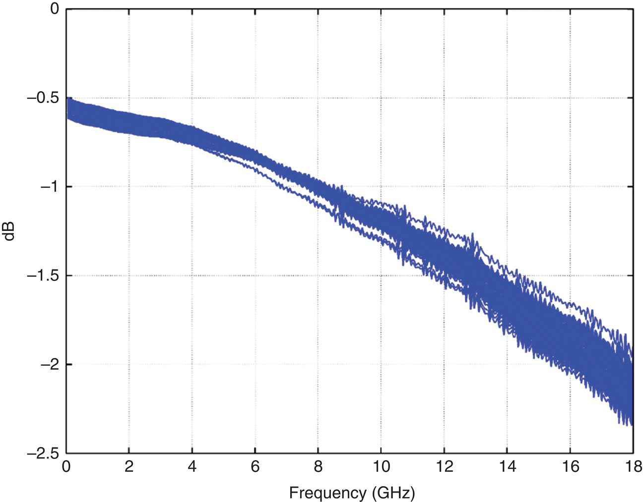
Figure 23.8 Insertion loss of hundreds of samples of a representative EMIB interconnect design.
Typically EMIB is used to connect two adjacent die. This results in a relatively short I/O channel that does not demand complex transceiver circuits to meet signal integrity requirements. Figure 23.9 shows an equivalent circuit example of an EMIB I/O channel. The driver is a simple CMOS inverter and the receiver does not have termination. When data switches from 0 to 1, the driver pumps current into the channel to charge all the capacitance loading from the channel and transceiver circuits. The consumed power is CV2 where C represents the total capacitance loading and V is the driver supply voltage. When data switches from 1 to 0, all the capacitive loading discharges, a process that does not consume power. Hence the overall clock data pattern has an energy efficiency of 0.5CV2, and a random data pattern has a power efficiency of 0.25CV2. If the total loading is less than 2 pF, the driver energy efficiency is less than 0.5 pJ b−1 at 1 V. Any reduction of the voltage can quadratically reduce the power consumption.

Figure 23.9 Simple I/O driver and unterminated receiver for EMIB interconnect channel. (a) Channel load charges when data switch from 0 to 1. (b) Channel load discharges when data switch from 1 to 0.
To demonstrate that the above described I/O channel and circuits can meet signal integrity requirements, results from eye diagram simulations at 2 Gbps performed for varying channel lengths are shown in Figure 23.10. A 12 mA CMOS inverter driver and 0.4 pF pad capacitance are assumed for both the driver and the receiver. The eye diagram is the predicted worst‐case eye based on the peak distortion analysis (PDA) [20, 21]. The results in Figure 23.10 show that a good eye opening can be achieved even with a 9.7 mm long channel that demonstrates the signaling performance capability of EMIB. Combined with the high I/O/mm capability of the technology, it is possible to achieve high bandwidth die‐to‐die channels using EMIB.

Figure 23.10 Eye diagrams of 2 Gbps signaling at channel lengths from 3.2 to 9.7 mm. Driver is a simple 12 mA inverter, receiver is unterminated, and both driver and receiver have 0.4 pF pad capacitance.
23.5 Conclusions
In this chapter, we present a description of the EMIB dense MCP technology that provides localized high density interconnects at a lower cost than competing technologies providing low power, high bandwidth interconnects. A high level process flow is shown along with the enabling technologies needed to realize the technology. EMIB is a proven technology utilizing a number of novel technological innovations. Measured signal integrity on test structures demonstrates that the EMIB technology is capable of supporting high bandwidth interconnects.
Acknowledgments
The authors would like to acknowledge Bob Starkston, John Guzek, Deepak Kulkarni, Chris Baldwin, Sanka Ganesan, Babak Sabi, Ken Brown, Chris Nelson, Chia‐Pin Chiu, Henning Braunisch, Aleks Aleksov, Ram Viswanath, Sriram Srinivasan, Hamid Azimi, Mostafa Aghazadeh, Koushik Banerjee, Omkar Karhade, Johanna Swan, Stefanie Lotz, and Nitin Deshpande from Intel for their contributions in evolving the EMIB concept from paper to reality. Discussions with Rajat Agarwal, Suresh Chittor, and Randy Osborne from Intel on memory directions are gratefully acknowledged.
References
- 1 Goto, H. (2015). http://pc.watch.impress.co.jp/img/pcw/docs/740/790/html/1.jpg.html (accessed 6 August 2018).
- 2 Bender, M.A., Berry, J.W., Hammond, S.D. et al. (2017). Two‐level main memory co‐design: multi‐threaded algorithmic primitives, analysis and simulation. Journal of Parallel Distributed Computing 102: 213–228.
- 3 International Solid‐State Circuits Conference (ISSCC) (2017). Trends. http://isscc.org/wp‐content/uploads/2018/06/2017_Trends.pdf (accessed 6 August 2018).
- 4 Mansuri, M., Jaussi, J. E., Kennedy, J. T. et al. (2013). A scalable 0.128‐to‐1Tb/s 0.8‐to‐2.6pJ/b 64‐lane parallel I/O in 32nm CMOS. Proceedings of the IEEE International Solid‐State Circuits Conference, San Francisco, CA, USA (2013), pp. 402–403.
- 5 Casper, B. (2011). Energy efficient multi‐Gb/s I/O: circuit and system design techniques. Workshop on Microelectronics and Electron Devices (WMED), Boise, ID, USA (22 April 2011).
- 6 O'Mahony, F., Balamurugan, G., Jaussi, J., et al. (2009). The future of electrical I/O for microprocessors. Proceedings of the IEEE Symposium on. VLSI Design Automation and Test (VLSI‐DAT) (April 2009), pp. 31–34.
- 7 https://www.jedec.org/standards‐documents/docs/jesd235a (accessed 6 August 2018).
- 8 http://www.skhynix.com/eng/product/dramHBM.jsp (accessed 6 August 2018).
- 9 https://www.altera.com/products/fpga/stratix‐series/stratix‐10/overview.html (accessed 6 August 2018).
- 10 Greenhill, D., Ho, R., Lewis, D. et al. (2017). A 14nm 1GHz FPGA with 2.5D transceiver integration. 2017 IEEE International Solid‐State Circuits Conference (ISSCC) Solid‐State Circuits Conference (ISSCC), 2017 IEEE International (February 2017), pp. 54–55.
- 11 Mahajan, R., Sankman, R., Patel, N. et al. (2016). Embedded multi‐die interconnect bridge (EMIB) – a high density, high band‐width packaging interconnect. Proceedings of the 66th Electronic Components and Technology Conference, Las Vegas, Nevada (June 2016), pp. 557–565.
- 12 Huemoeller, R. and Zwenger, C. (April 2015). Silicon wafer integrated fan‐out technology. Chip Scale Review 19 (2).
- 13 Oi, K., Otake, S., Shimizu, N. et al., “Development of new 2.5D package with novel integrated organic interposer substrate with ultra‐fine wiring and high density bumps.” Proceedings of the 2014 IEEE 64th Electronic Components and Technology Conference, Orlando, pp. 348–353.
- 14 Mahajan, R. and Sane, S. Microelectronic package containing silicon patches for high density interconnects, and method of manufacturing same. US patent no. 8,064,224.
- 15 Braunisch, H., Aleksov, A., Lotz, S., and Swan, J. (2011). High‐speed performance of silicon bridge die‐to‐die interconnects. Proceedings of the IEEE Conference on Electrical Performance of Electronic Packaging and Systems (EPEPS), San Jose, CA, 23–26 October 2011, pp. 95–98.
- 16 Robert, S., Mallik, D., Guzek, J. et al. Localized high density substrate routing. US patent no. 9,136,236.
- 17 Sunohara, M., Tokunaga, T., Kurihara, T., and Higashi, M. (2008). Silicon interposer with TSVs (through silicon vias) and fine multilayer wiring. Proceedings of the IEEE Electronic Components and Technology Conference (ECTC), Lake Buena Vista, FL (27–30 May 2008), pp. 847–852.
- 18 https://www.amkor.com/go/technology/slim (accessed 6 August 2018).
- 19 Eitan, A. and Hung, K‐Y (2015). Thermo‐compression bonding for fine‐pitch copper‐pillar flip‐chip interconnect – tool features as enablers of unique technology. Proceedings of the IEEE 65th Electronic Components and Technology Conference (ECTC) (May 2015), pp. 460–464.
- 20 Proakis, J.G. (1995). Digital Communications, 3e, 602–603. Singapore: McGraw‐Hill.
- 21 Casper, B.K., Haycock, M., and Mooney, R. (2002). An accurate and efficient analysis method for multi‐Gb/s chip‐to‐chip signaling schemes. IEEE Symposium on VLSI Circuits Digest of Technical Papers (June 2002), pp. 54–57.