
6
M‐Series™ Fan‐Out with Adaptive Patterning™
Tim Olson and Chris Scanlan
Deca Technologies
6.1 Technology Description
M‐Series is a chip‐first, face‐up fan‐out wafer‐level packaging (FO‐WLP) technology with a unique structure wherein the semiconductor device active surface and vertical sidewalls are fully encapsulated within the epoxy molding compound (EMC) with device interconnect enabled by Cu studs through the EMC layer as shown schematically in Figure 6.1a and in actual cross section [1] in Figure 6.1b

Figure 6.1 (a) Schematic of M‐Series FO‐WLP. (b) Actual cross section of M‐Series FO‐WLP.
The EMC layer between the active region of the chip and the end electronic appliance printed circuit board (PCB) provides an intermediate stress buffer that has proven to significantly extend board‐level reliability (BLR) as compared with conventional wafer‐level chip‐scale packaging (WLCSP) with only polyimide or polybenzoxazole (PBO).
Figure 6.2 shows a JEDEC condition G BLR temperature cycle comparison of a 6 mm × 6 mm semiconductor device in a conventional WLCSP versus the same chip in a 6.25 mm × 6.25 mm M‐Series fan‐out package with SAC405 solder balls. All samples utilized 0.35 mm pitch with approximately 8% depopulation on the WLCSP devices and approximately 15% on M‐Series. The additional LF35 (Sn/Ag1.2/Cu0.5/Ni0.05) solder ball data was included since it is an alternative solder used on WLCSP in drop or shock‐sensitive applications. LF35 has not been tested on the M‐Series structure.

Figure 6.2 BLR comparison of M‐Series versus WLCSP.
Adaptive patterning was developed in conjunction with M‐Series to overcome the inherent inaccuracies associated with creating a composite wafer or panel consisting of individual devices embedded within EMC or alternate materials. Adaptive patterning includes measurement of each die location within the panel, creation of a complete panel design that perfectly fits the as‐built fan‐out panel, and application of the unique design to each panel. Through adaptive patterning, simple devices can be constructed cost‐effectively, while complex and multicomponent devices can be assured of high yields in manufacturing. Figure 6.3 provides a high level overview of the adaptive patterning methodology [2]; a detailed description follows in Section 6.5.
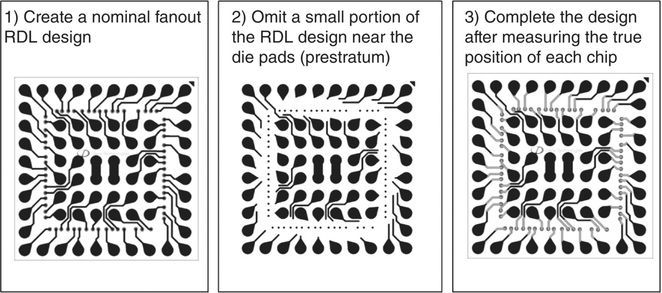
Figure 6.3 Adaptive patterning methodology using adaptive routing.
M‐Series has been qualified by multiple semiconductor companies with silicon devices fabricated in 150–350 nm geometries on 200 mm wafers as well as 14–65 nm technologies on 300 mm for leading cellular phone handset producers.
6.2 Basic Package Construction
M‐Series is fundamentally an embedded chip fully molded fan‐out technology that blends the benefits of classic lead frame or laminate packaging in terms of providing complete molded protection to the active semiconductor device while utilizing the massively parallel processing capability of wafer‐ or panel‐level processing to create the interconnect layers. The basic structure with a single layer of RDL (Cu redistribution layer) is shown in Figure 6.4.

Figure 6.4 Basic package construction of M‐Series.
As compared with traditional fan‐in (WLCSP) and conventional fan‐out [3, 4], M‐Series provides several important reliability and manufacturability benefits. A primary reliability benefit includes lowering of e‐chip‐board interaction (CBI) stresses applied to the device [5] as a result of the molded stress buffer layer between the active region of the semiconductor device and the PCB acting in a similar manner to a laminate substrate in a classic flip‐chip ball grid array (BGA) package. The M‐Series molded stress buffer layer has already proven to provide superior BLR performance exceeding a 200% improvement as compared with traditional fan‐in WLCSP technologies as shown in Figure 6.2. Since conventional fan‐out technologies utilize organic spin‐on polymers as the only stress buffer between the active device and the PCB, similar to fan‐in WLCSP, e‐CBI stresses are expected to be significantly higher as compared to M‐Series.
A second key benefit of M‐Series versus conventional fan‐out structures is elimination of EMC from the physical vapor deposition (PVD) process while completing first‐level interconnect to the aluminum bond pads wherein the process window is typically limited to ensure low contact resistance (Rc). With M‐Series, the Cu stud‐to‐Al bond pad connection is performed on the native silicon wafer, allowing a much wider process window to ensure low Rc prior to dicing and chip attach of the devices into a reconstituted panel. Panel‐level interconnects, typically a TiCu PVD seed followed by electroplated Cu, are formed to the Cu surface of the stud, which is opened up during the topside planarization. The Cu‐to‐Cu interconnect scheme in panel form enables a more robust PVD process with a much wider operating window.
A third benefit of M‐Series versus conventional fan‐out structures is the embedding of sawn device edges within the EM preventing residual metallic buildup from laser grooving or dicing potentially protruding through the organic spin‐on polymer dielectric over the surface of the silicon to EMC interface. An example of metallic buildup protruding through the dielectric on a conventional fan‐out structure causing electrical shorting failures at the device edge is shown in Figure 6.5 (courtesy of Advanced Semiconductor Engineering [ASE]).

Figure 6.5 Conventional fan‐out structure with electrical shorting failure.
Source: courtesy of ASE.
A fourth benefit of M‐Series versus conventional fan‐out is the planarized structure that eliminates the discontinuity from the active device surface to the EMC surface, resulting in nonplanarity of the first dielectric layer. In a structure where two semiconductor devices are placed in close proximity to each other, the resulting topography from silicon surface to EMC surface in conventional fan‐out can be significant as shown in Figure 6.6.

Figure 6.6 Nonplanarity of silicon to EMC surface in conventional fan‐out.
Source: courtesy of ASE.
The resulting 5.5 μm of dielectric nonplanarity as shown in Figure 6.6 severely limits the ability of scaling conventional fan‐out to fine lines and spaces (2 μm and below) given the need for tightly controlled depth of focus (DOF) in the lithography process.
In contrast, the planarized nature of M‐Series as shown in Figure 6.7 allows for straightforward scaling to 2 μm and below since planarization is built into the process flow. For extremely fine future submicron lines, a potential planarization enhancement with more advanced polishing technology may be implemented to reduce the current surface Ra (average surface roughness) if required.

Figure 6.7 Planar surface over silicon device to EMC interface on M‐Series.
M‐Series is ideally suited for fan‐in WLCSP applications requiring enhanced BLR capabilities as well as for fan‐out applications where the package size is within approximately two times the area of the chip, essentially a fan‐out ratio (package area to die area) of 2.0 or less. While technically capable for much larger fan‐out ratios, classic packaging technologies based on laminate or lead frame substrates will likely provide a more cost‐effective solution within the coming few years. Over time, it is forecasted that large panel M‐Series fan‐out will be able to compete on cost with much larger fan‐out ratios.
The limits of package size for M‐Series have not yet been fully explored as of this writing. However, the fundamental structure and materials set should be extendable for multi‐die and component modules approaching 2500 mm2 such as integration of advanced graphics processors with supporting high‐speed, high bandwidth memory chips surrounding their periphery.
M‐Series applications as intermediate pitch expanders for large die sizes in advanced silicon nodes are also foreseen wherein device bond pad pitch is so dense that direct flip‐chip attach may not be feasible or cost‐effective due to limitations in escape routing within organic substrates. In this application, the M‐Series package becomes a pitch‐expanding pseudo‐die that would include micro bumps, enabling flip‐chip mounting to a laminate substrate to complete the package‐level assembly.
6.3 Manufacturing Process Flow and BOM
M‐Series utilizes a semiconductor wafer manufacturing environment including advanced lithography, PVD, electroplating, etching, cleaning, and visual inspection methodologies consistent with fabricating wafer‐level packaging as well as the final back‐end‐of‐line (BEOL) interconnect layers within semiconductor device fabs.
The basic process flow for M‐Series shown in Figure 6.8 begins with the “wafer prep” segment, which includes the fabrication of Cu studs on the native semiconductor wafer by sputter deposition of seed layers, patterning of a thick photoresist, electroplating Cu studs, performing strip, and etch of the photoresist and seed layers followed by backgrind and singulation to provide a thinned and diced wafer ready for pick and place of each device.

Figure 6.8 M‐Series process flow for a fully molded FO‐WLP.
In the second segment, called panelization, the singulated devices are attached faceup to a reusable temporary carrier at the desired fanned‐out pitch. The carrier and chips are then overmolded to create a plastic panel, currently in the form of a SEMI standard 300 mm wafer with development underway on a large panel format to be discussed later. The plastic panel is then debonded from the carrier and post‐mold cured. Top grind is performed on the panel to reveal the Cu studs and create a highly planar surface. Finally, an optical scanner is used to measure the precise x,y location and theta rotation of each device on the panel to enable the adaptive patterning technique described in Section 6.5.
Following panelization, wafer‐level fan‐out processing is performed on the molded panel. This includes patterning and curing one or more polymer layers as well as patterning and electroplating one or more Cu RDL or under‐bump metallization (UBM) layers. Ball drop and reflow are then performed.
For package finishing, panel backgrind is performed for final thinning and a backside laminate is applied, followed by laser mark, package saw, and tape and reel.
6.4 Design Features and System Integration Capability
The standard M‐Series cross‐sectional stack‐ups are shown in Figure 6.9. The M4 stack‐up contains a total of four patterned layers (polymer 1, Cu RDL, polymer 2, and UBM). The M6 structure contains an additional RDL and polymer layer for a total of six patterned layers.

Figure 6.9 Standard M‐Series cross‐sectional stack‐ups.
Several different via stack‐up options are possible within the M‐Series fan‐out buildup structure. In many designs a staggered via structure is employed as showed in Figure 6.10. In this case, the vias connecting Cu RDL and UBM layers are offset with respect to each other.

Figure 6.10 M‐Series buildup with staggered vias.
It is possible to position the UBM and BGA ball directly over a Cu stud. Figure 6.11 shows this embodiment.

Figure 6.11 M‐Series buildup with UBM and BGA ball directly over a Cu stud.
Via‐in‐pad structures with the via connecting the UBM capture pad to the first RDL layer (in the case of the M6 stack‐up) or the Cu stud (in the case of the M4 stack‐up) are also possible as shown in Figure 6.12.

Figure 6.12 M‐Series buildup with UBM via in RDL2 via.
Finally, fully stacked vias with the UBM and solder ball positioned directly over and directly connected to one or more Cu studs through both RDL layers are possible as shown in Figure 6.13.

Figure 6.13 M‐Series buildup with fully stacked vias.
M‐Series provides mechanical isolation between the solder ball and Si die by providing a rigid molded epoxy layer between the die and fan‐out buildup structure. As a result, there is no design rule restriction with respect to placement of BGA balls in the “die shadow” region of the package. BGA pads can be placed directly over the die edge as shown in Figure 6.14.

Figure 6.14 M‐Series BGA view showing BGA balls over die shadow shown as black line.
Since the M‐Series structure uses a plated Cu interconnect without solder to connect the die bond pads to the fan‐out routing layer, there is a lot of flexibility on designing the Cu stud layer. Different interconnect sizes and shapes can be used within the same design as shown in the die layout drawing in Figure 6.15.

Figure 6.15 M‐Series BGA view showing BGA balls over die shadow in light.
3D package designs are also possible using the M‐Series structure. Common 3D structures include peripheral package on package (PoP) as shown in Figure 6.16 and fan‐in PoP as shown in Figure 6.17.

Figure 6.16 M‐Series peripheral PoP schematic.

Figure 6.17 M‐Series fan‐in PoP schematic.
A summary of M‐Series critical design rules, roadmap design rules, and design features is given in Table 6.1.
Table 6.1 M‐Series design rules.
| M‐Series design feature roadmap | ||
| Design feature | 2018 | In development |
| Cu stud layer | ||
| Maximum stud thickness (μm) | 35 | 50 |
| Minimum stud thickness (μm) | 25 | 10 |
| Minimum stud diameter (μm) | 30 | 10 |
| Minimum stud spacing (μm) | 12 | 5 |
| Minimum stud pitch (μm) | 42 | 15 |
| First fan‐out polymer via layer | ||
| Minimum via diameter (μm) | 15 | 5 |
| Minimum Cu stud enclosure (μm) | 7.5 | 3 |
| Minimum PI thickness – first layer (μm) | 6 | 3 |
| Maximum PI thickness (μm) | 12 | 12 |
| Fan‐out RDL layers | ||
| Minimum trace width (μm) | 8 | 2 |
| Minimum trace space (μm) | 8 | 2 |
| Maximum RDL thickness (μm) | 11 | 11 |
| Minimum via 1 enclosure (μm) | 7.5 | 3 |
| RDL layers | 2 | 4 |
| Final fan‐out polymer via layer (under UBM) | ||
| Maximum PI thickness (μm) | 12 | 12 |
| Adaptive via truncation (%) | 25 | 50 |
| Via 2 – RDL enclosure (μm) | 15 | 5 |
| UBM layer | ||
| Maximum UBM thickness (μm) | 9 | 20 |
| Minimum BGA pitch (μm) | 350 | 250 |
| Package outline | ||
| Minimum die thickness (200 mm) (μm) | 170 | 100 |
| Max fan‐out ratio | 2.5 | 3.5 |
| Minimum die to package edge (μm) | 60 | 30 |
| Max die edge length (mm) | 8 | 12 |
| Max package edge length (mm) | 10 | 18 |
| Minimum BSL thickness (μm) | 25 | 15 |
| Total package thickness (mm) | 0.45 | 0.25 |
| Land side caps | — | ✓ |
| 3D features | ||
| Minimum TMIa pitch (μm) | — | 100 |
| Minimum TMI diameter (μm) | — | 50 |
| Minimum TMI spacing (μm) | — | 50 |
| TMIa termination (peripheral PoP) | — | SnAg |
| TMI recess (peripheral PoP) (μm) | — | 40 |
| Topside routing layer count | — | 2 |
| Topside routing minimum feature size (μm) | — | 5 |
| Topside land termination (fan‐in PoP and SiP) | — | NiAu |
| Embedded passives | — | ✓ |
| EMI shielding | — | ✓ |
| Die count | 3 | 6+ |
| 1.5 D routing (routing in Cu stud layer) | ||
| Minimum trace width (μm) | 25 | 15 |
| Minimum trace space (μm) | 25 | 15 |
| Maximum routing density (% of package area) | 40 | 60 |
| Minimum PM0 enclosure (μm) | 8.5 | 5 |
a TMI, through‐mold interconnect.
6.5 Adaptive Patterning
One of the main challenges that has prevented the widespread adoption of wafer‐level fan‐out technology is yield loss due to imperfect alignment of fixed lithography masks to shifting devices during manufacturing. Die shift is an accumulation of die position error from chip‐attach equipment tolerances, as discussed in the previous section, and movement during molding as shown schematically in Figure 6.18. A portion of the movement due to molding can be predicted and compensated for during die placement. However, equipment and process tolerances give each die a random and unpredictable offset and rotation. Although higher throughput chip‐attach equipment can reduce manufacturing costs, the increased throughput typically results in decreased placement accuracy. Increased die shift is a major contributor to yield loss, and the wider variance limits design rules. Previously, this presented an engineering trade‐off. For M‐Series, Deca Technologies invented a technology called adaptive patterning [6] to overcome the die‐shift problem without compromising chip‐attach throughput or design rules and to further enable high yield multi‐die system‐in‐package (SiP) devices.

Figure 6.18 Illustration of die shift from pick and place tolerances and molding.
Rather than attempting to minimize die placement tolerance and compromising design rule density, adaptive patterning takes a novel approach: adjust the lithography pattern in response to the die placement [1]. First, the actual position of each die after pick and place and molding is measured using a high throughput optical inspection system. This produces a dataset of the final XY translation and rotation for each die. This dataset is processed by a custom software system to produce a unique lithography pattern for each package that accounts for the as‐chip‐attached and as‐molded die shift. Finally, for each buildup layer, a custom pattern generated for each FO‐WLP device is automatically applied within the photolithography system. By uniquely generating a lithography pattern for each package, the adverse effects of unavoidable random die shift can be avoided. There are several techniques that can be used to generate the per‐package lithography patterns.
The first technique, called adaptive alignment, dynamically translates and rotates elements of each package layer to match the measured die shift. In this technique and others, the design must be prepared by splitting it into portions, called prestratums, as shown in Figure 6.19. Each prestratum contains elements of the design, such as vias and RDL traces, that can be separately translated and rotated per package. In adaptive alignment, one prestratum, consisting of the first via layer openings and the copper RDL pattern, is rotated and translated to exactly match the measured die position. In this way, the first via layer openings are precisely aligned to the die contacts. Another prestratum is untranslated and unrotated and thus remains aligned to the package. The package‐aligned prestratum contains the under‐bump via (UBV) openings, the UBM pads, and the saw street openings for all polymer layers. In this way, the BGA grid pitch and alignment are unaffected.
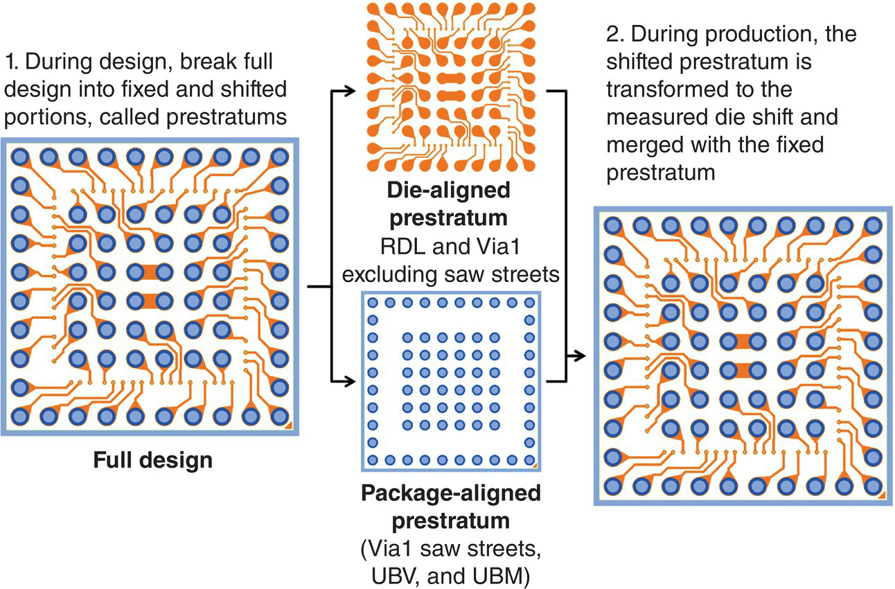
Figure 6.19 The generation of unique per‐package lithography patterns by adaptive alignment.
Die shift is accounted for in the interface between the RDL and the UBV layer. Effectively, the RDL capture pad is allowed to move underneath the UBV opening within an allowable range determined by the design rules. In this case, the critical rule is the enclosure of the UBV by the RDL, or the distance between the edge of the UBV and the surrounding RDL capture pad. As shown in Figure 6.20, the RDL to UBV pad stack must be designed with sufficient enclosure to ensure that the UBV overlaps the RDL capture pad over the entire expected range of die shifts. Typically, the UBV diameter is reduced by the expected die shift on each side.

Figure 6.20 For adaptive alignment, the PRDL‐UBV interface must be designed with sufficient enclosure for the expected range of die shifts.
In some cases, such as high current devices, decreasing the UBV area can be undesirable, and increasing the RDL capture pad diameter is not always an option. For these cases, Deca has developed another technique, called adaptive via truncation (AVT), wherein the UBV is minimally changed to account for die shift. Rather than designing the pad stack with extra enclosure, AVT dynamically truncates the UBV area to meet the enclosure design rule. With this technique, rather than reducing the UBV opening diameter during design, the UBV area is reduced dynamically and only by the necessary amount for each specific die shift. After truncation, shown in Figure 6.21, the majority of via area is preserved, as only a small crescent‐shaped portion is removed for even the worst‐case die shift.

Figure 6.21 Adaptive via truncation maximizes UBV area with minimal changes to the design. The left figure shows the nominal design with zero die shift. The middle figure highlights the truncated UBV area with a left and upward die shift; the right figure illustrates truncation for a right and downward die shift.
Another technique, called adaptive routing, compensates for die shift by dynamically rerouting portions of RDL traces on each package. To prepare a design for adaptive routing, small portions are removed from the RDL traces that connect to the capture pads for the first via layer as shown in Figure 6.22. Their removal leaves sufficient space for the adaptive patterning software system to dynamically reroute the traces after the vias and capture pads are translated and rotated to align with the die.

Figure 6.22 Adaptive routing combines the die‐aligned and package‐aligned prestratums with dynamically generated routing from the partial RDL pattern to the via opening capture pads; a small section of each trace is removed to leave room for the first via layer openings and capture pads to shift with the die.
As in adaptive alignment, the design is divided into multiple portions, called prestratums, as shown on the left side of Figure 6.22. In this case, the die‐aligned prestratum does not contain the entire RDL pattern, but rather just the via openings and RDL capture pads. The package‐aligned prestratum contains the rest of the RDL patterning, including the partially complete traces, the UBV openings, the UBM pads, and the polymer layer saw street.
During manufacturing, the die‐aligned and package‐aligned prestratums are merged using the measured die positions. As in adaptive alignment, the BGA grid and pitch remain unaffected. Adaptive routing compensates for die shift by dynamically generating new RDL trace patterns that connect the partial RDL pattern to the translated and rotated capture pads for the first via layer. As shown on the right in Figure 6.22, the software system generates short RDL trace portions that meet design rules and can account for large die shifts. The capability of adaptive routing to compensate for die shift is limited only by the amount of clearance available for the first via capture pads to shift and for the subsequent rerouting.
Adaptive patterning technology has also been extended to multi‐die SiP designs, providing an improved capability for high yield integration. For traditional embedded fan‐out technologies, integrating multiple die poses a yield risk because each die has a random independent shift, but all die must be within the tolerance of one fixed lithographic pattern. This requires design rules with wider tolerances to account for multiple die shifts or results in yield loss. With adaptive patterning, the design can be adjusted to independently accommodate the expected range of shifts for each die.
As shown in Figure 6.23, the design methodology for multi‐die integration combines the adaptive alignment and adaptive routing techniques. A separate die‐aligned prestratum for each die contains the first via layer openings and a portion of the copper RDL layout. The die‐to‐die connections are completed using adaptive routing between the die‐aligned prestratums, accommodating the shift of both die simultaneously. In this particular example, it was also advantageous to keep a portion of the RDL layout in the fixed, or package‐aligned, prestratum (the blue traces shown in Figure 6.21) and connect to it with adaptive routing. As in single‐die adaptive alignment, the BGA grid and pitch remain fixed.

Figure 6.23 Adaptive alignment can be combined with adaptive routing for multi‐die designs. Shown in step A, the UBM and UBV pad stacks are fixed with respect to the package edge. Then, in step B, a prestratum including a portion of the RDL and via 1 openings is aligned to each die using adaptive alignment. In many designs, it is beneficial to keep a portion of the RDL fixed with respect to the package edge, such as the partial traces between the die in step C. Finally, in step D, adaptive routing is used to complete die‐to‐die connections.
Through the use of one or more of these techniques, adaptive patterning offers a uniquely robust solution to the die‐shift problem, overcoming a major yield challenge in traditional embedded fan‐out packaging technologies. In addition, the technology enables cost‐effective production using high throughput chip‐attach machines that can make FO‐WLP economical even for smaller die sizes.
6.6 Manufacturing Format and Scalability
A large panel format M‐Series has been the goal since its inception. With Deca’s foundation of largely non‐semiconductor equipment, creating equipment and processes for a large panel format was foreseen as relatively straightforward. M‐Series utilizes several processes derived from solar wafer fabrication including PVD seed, Cu electroplating, photoresist strip, seed layer etch, and high pressure cleans. Figure 6.24 provides a high level mapping of solar cell wafer processing versus Deca WLCSP processes, which are utilized in both conventional fan‐in WLCSP and M‐Series production.

Figure 6.24 Similarities of solar cell wafer process versus Deca’s WLCSP process.
In 2012, Deca established a 600 mm × 600 mm square format for M‐Series and began development of the materials, equipment, and processes to support future high volume production. A 600 mm square was chosen for the capability to cut the panels into 300 mm × 300 mm square segments following wafer processing for the initial production implementation. The resulting 300 mm square subpanels were planned to allow utilization of existing 300 mm round wafer probe electrical test assets with minor equipment upgrades. A photo of an actual 600 mm panel post chip attach that enables 300 mm quartering post fan‐out processing is shown in Figure 6.25.

Figure 6.25 The 600 mm × 600 mm panel configured for quartering to 300 mm squares.
600 mm allows the further flexibility of segmenting the panel into 200 mm squares following wafer processing for utilization of existing 300 mm round BEOL equipment in the early development phase. The 200 mm subpanels are within the maximum square dimension that can be mounted on standard 300 mm wafer saw rings and fall below the 212 mm maximum dimension that can spin within a 300 mm diameter. Figure 6.26 provides images of an actual 300 mm round initial production panel as well as an early large panel prototype through top grind.

Figure 6.26 M‐Series manufacturing formats.
ASE and Deca are cooperating to establish 600 mm production capability with plans to implement capacity in both companies. Current engineering work has demonstrated that the 300 mm processes, structure, and direct material set scale successfully to 600 mm, allowing flexibility to produce identical finished products for end customers from either 300 mm round or 600 mm square format.
It is contemplated that the 600 mm format will be carried through the entire manufacturing process to package singulation once final test and back‐end process and equipment capabilities have been developed.
6.7 Robustness and Reliability Data
M‐Series has been fully qualified according to JEDEC and OEM reliability standards for mobile phone applications. As of March 2018, M‐Series packages up to 8 mm × 8 mm body size and fan‐out ratio as low as 1.05 have been qualified through MSL 1 component level and BLR requirements. Table 6.2 shows results for package sizes ranging from 5 to 8 mm per side across four different wafer foundries and three device technology nodes. Since M‐Series was designed to meet MSL 1 preconditioning requirements, more extensive package‐level testing was completed through larger sample sizes as compared with MSL 3.
Table 6.2 M‐Series reliability results.
| M‐Series package‐level reliability results | |||||||
| MSL 1 | MSL 3 | ||||||
| Device | Si node | Fab | Test type | TCG | uHAST | TCG | uHAST |
| A | 150 nm | 1 | Electrical | 0/216 | 0/220 | 0/68 | 0/66 |
| CSAM | 0/216 | 0/220 | 0/68 | 0/66 | |||
| 2 | Electrical | 0/240 | 0/240 | 0/80 | 0/80 | ||
| CSAM | 0/240 | 0/240 | 0/80 | 0/80 | |||
| B | 40 nm | 3 | Electrical | 0/400 | 0/400 | 0/240 | 0/240 |
| CSAM | 0/400 | 0/400 | 0/240 | 0/240 | |||
| C | 14 nm | 4 | Electrical | 0/240 | 0/240 | 0/80 | 0/80 |
| CSAM | 0/240 | 0/240 | 0/80 | 0/80 | |||
| Test conditions | MSL 1 and MSL 3 – JEDEC/IPC joint industry standard J‐STD‐020A | ||||||
| TCG = 1000 cycles air to air temperature cycling from −40 to +125 °C | |||||||
| uHAST = 96 h at 130 °CC in 85% RH, 33.3 psia | |||||||
| Electrical = open, short, or leakage failures | |||||||
| CSAM = visible delamination as detected with 20 μm resolution | |||||||
The significant improvement in BLR temperature cycle capability of M‐Series versus conventional WLCSP and by similarity conventional fan‐out constructed only with spin‐on dielectric stress buffer layers was shown in Figure 6.2.
6.8 Electrical Test Considerations
As mentioned in Section 6.6, M‐Series is planned to be produced in both 300 mm round and 600 mm square formats in high volume production. With the M‐Series structure, 300 mm round warpage is maintained within the specification limits of ±3 mm. Multiple existing commercially available 300 mm test probe handler suppliers can accommodate this level of warpage, allowing M‐Series to be tested or probed as a 300 mm wafer.
Quartering of 600 mm square panels post fan‐out processing into 300 mm squares allows the potential for upgrading 300 mm round probe handlers to process the panels as shown schematically in Figure 6.27.

Figure 6.27 300 mm round to 600 mm by 600 mm square panel.
Given the fully molded structure of M‐Series, singulated component final test is straightforward. The molded stress buffer layer over the active device region, molded sidewall protection, and epoxy‐covered backside of the device allow it to also be handled with existing commercially available test handlers designed for singulated laminate BGAs.
6.9 Applications and Markets
The first applications to adopt M‐Series are chipsets for mobiles phones and other miniaturized electronic systems such as wearable electronics. Within the mobile phone chipset, M‐Series has been qualified on devices such as power management ICs (PMICs), codec ICs, and RF transceivers. M‐Series in a PoP structure is planned to be employed as the bottom package for application processors. Multi‐chip M‐Series will be used for a variety of SiP applications including IoT modules containing RF functionality, sensors, and processing. A roadmap capability of M‐Series is fine‐pitch (< 2 μm line and space) high density multilayer interconnect enabling a cost‐effective alternative to silicon interposers. Applications for high density M‐Series include heterogeneous systems on a chip, split‐die architectures, and graphics or microprocessor integration with high bandwidth memory.
Acknowledgment
The authors would like to express their sincere appreciation to Craig Bishop as well as Boyd Rogers and Cliff Sandstrom who were instrumental in creating adaptive patterning and the overall M‐Series technology, respectively. We also appreciate Craig’s contribution of the adaptive patterning section of this chapter.
References
- 1 Rogers, B., Olson, T., and Scanlan, C. (2013). Implementation of a fully molded fan‐out packaging technology. IWLPC Proceedings (November 2013).
- 2 Bishop, C., Olson, T., and Scanlan, C. (2016). Adaptive patterning design methodologies. 2016 IEEE 66th Electronic Components and Technology Conference (ECTC), Las Vegas, NV (2016), pp. 7–12.
- 3 Brunnbauer, M., Fürgut E., Beer, G., and Meyer, T. (2006). Embedded wafer level ball grid array (eWLB). Electronics Packaging Technology Conference 8th Proceedings (December 2006).
- 4 Keser, B., Amrine, C., and Leal G. (2007). The redistributed chip package: a breakthrough for advanced packaging. 2007 Electronic Components and Technology Conference, pp. 286–291.
- 5 Zhao, W., Nakamoto, M., Dhandapani, K. et al. (2017). Electrical chip‐board interaction (e‐CBI) of wafer level packaging technology. IMAPS Advancing Microelectronics (November/December 2017).
- 6 Scanlan C., Rogers, B., and Olson, T. (2012). Adaptive patterning for panelized packaging. IWLPC Proceedings (November 2012).