
8
Embedded Silicon Fan‐Out (eSiFO®) Technology for Wafer‐Level System Integration
Daquan Yu
Huatian Technology (Kunshan) Electronics Co.,Ltd., Economic & Technical Development Zone, Kunshan, Jiangsu, China
8.1 Technology Description
The demand for miniaturized package size, higher performance and integration density, lower power consumption, and lower manufacturing cost drives the development of various new packaging technologies. Among those new packaging technologies, the fan‐out wafer‐level package (FO‐WLP) has emerged as a successful technology in providing the solution to fulfill the abovementioned requirements. FO‐WLP has also become a key‐enabling technology for multi‐chip and 3D system integration [1]. As one type of FO‐WLP, embedded silicon fan‐out (eSiFO) technology, in which silicon instead of molding compound was used as the fan‐out area, was proposed in 2015 [2]. It is a chip‐first and face‐up process, eliminating molding, temporary bonding, and debonding process and has been in volume production not only for single‐die package but also for multi‐die system‐in‐package (SiP) applications.
8.2 Basic Package Construction
Figure 8.1 shows the structure of an eSiFO package. In the package, known good die (KGD) were embedded in a silicon carrier, and the microgaps between the die and silicon carrier were filled by polymer. The die and silicon carrier reconstruct a surface for the routing of redistribution layers (RDL) and fabrication of solder balls. The main difference between eSiFO® and the typical FO‐WLP is that there is no epoxy molding compound (EMC) in eSiFO package.

Figure 8.1 Schematic view of the embedded silicon fan‐out (eSiFO) structure.
There are a number of advantages of the eSiFO package. The wafer warpage is very small during the manufacturing process since a silicon wafer is used as the reconstruct substrate. Therefore, wafer handling challenges and misalignment in lithography during the manufacturing process can be avoided [3]. The process is simple since there is no molding, temporary bonding, and debonding requirement. As a mature wafer‐level process, fine‐pitch high density RDL manufacturing is more easily built on a silicon wafer compared with an EMC wafer [1]. In addition, a small form factor can be achieved especially for SiP since multiple dies can be put close together and connected via fine‐pitch RDL. Furthermore, an ultrathin package of 150 μm can be achieved by thinning the wafer at the end of the packaging process. The ultrathin package is very important to achieving thinner smartphones and wearable electronics.
8.3 Manufacturing Process Flow
Typically, there are five major steps for FO‐WLP including KGD reconstruction, molding, debonding, wafer‐level RDL, and back‐end processing such as grinding, laser marking, and package singulation [1, 4]. From the process point of view, it is very troublesome to handle the EMC wafer, which usually has a large warpage since the coefficient of thermal expansion (CTE) of the EMC is largely different from the silicon chip. In addition, the manufacturing of fine‐pitch RDL on the EMC surface is also difficult as the poor coplanarity of die to mold will distort fine width and affect the RDL line continuity [5].
The process flow for eSiFO® package manufacturing is illustrated in Figure 8.2 [6]. Firstly, a silicon wafer was used to form cavities with a certain depth. A dry etch process by Bosch was used for cavity formation [7]. Secondly, thin dies with designed thickness were picked and placed into the cavities. After attachment of KGD, what is termed a “reconstructed wafer” was the result. Thirdly, the microgaps between the die and silicon carrier were filled with polymer, and the surface of the reconstructed wafer was passivated at the same time. Fourthly, the pads on die were opened by a lithography and development process. Fifthly, RDL was fabricated by standard process including seed layer deposition, photoresist (PR) formation, plating, PR strip, and seed layer etching. Then final passivation was performed. After ball grid array (BGA) formation, wafer thinning, and dicing, finally, an eSiFO package was fabricated.

Figure 8.2 Process flow of eSiFO package manufacturing.
Both 8 and 12 in. wafer processes for eSiFO were developed. At first, the cavities with vertical sidewall for die embedding were formed by the Bosch process. An inductively coupled plasma (ICP) source reactor is used, and the gases used in the Bosch process are SF6 and C4F8. For through‐silicon via (TSV) formation, silicon etch is quite mature since the etching area is small. However, the etching of large silicon cavities with good total thickness variation (TTV) is challenging. In addition, a smooth bottom surface without any grass, the term for blades of Si at the bottom of the cavity, or bumps was required to prevent die tilt and cracks during die attach process, which were formed due to the residual passivation during Bosch process [7] and particle contamination. For device die thickness, thinning to 60, 80, and 100 μm is possible. For 100 μm die thickness, the depth of the cavities on the wafer was set as 107 μm. Figure 8.3 shows a cross‐sectional view of a cavity for die embedding. The sidewall and bottom of the cavity are quite smooth. There are no “grass” or “bumps” on the bottom. The footing, the term for the angle where the sidewall meets the bottom of the cavity, variation in a single cavity is less than 5 μm without counting the region 15 μm away from the sidewall, to ensure the coplanarity of the embedded die and carrier. A flat bottom with ~1 μm roughness is achieved, which is suitable for die attachment.

Figure 8.3 Cross‐sectional view of the cavity after process optimization: (a) profile and (b) bottom.
A pick and place tool was used for chip to wafer attachment with an accuracy of ±4 μm. A die attach film (DAF) was applied to the backside of the die at wafer level, which is used to ensure fully bonding between the die and the silicon carrier without void. After die attachment, the wafer was hard‐baked for the curing of adhesive film. As shown in Figure 8.4, two reconstructed silicon wafers were formed before polymer filling. The gaps between die and silicon carrier are not visible.

Figure 8.4 Eight inch reconstructed wafers with different die sizes: (a) 2 mm × 2 mm and (b) 7 mm × 7 mm.
The filling of the trenches between the die and silicon carrier was a key process for eSiFO. A vacuum film lamination process was developed. The trench was filled without voids or cracks. Trenches in ~110 μm depth with 15, 20, 30, and 50 μm width after die attach were tested for polymer filling process. As shown in Figure 8.5, void‐free filling of the trenches was achieved.

Figure 8.5 The polymer filling of the trench with different widths: (a) 15 μm and (b) 50 μm.
Based on the current development of process, for eSiFO® package, a minimum opening size of 30 μm on first passivation, formed by the polymer filling process, can be achieved. A minimum line width of 15 μm for two RDL was developed for multi‐die integration, as shown in Figure 8.6. A Ni/Au layer was plated as under‐bump metallurgy (UBM) for BGA after the RDL process.

Figure 8.6 Two‐layer RDL for multi‐die integration.
To prove the concept of eSiFO, a 3.3 mm × 3.3 mm package with 0.4 mm pitch BGA was fabricated [6]. In the package, there is one layer of Cu RDL with a thickness of 3 μm and a minimum line width of 14 μm. The die size is 1.96 mm × 2.36 mm with a pad pitch of 90 μm. Figure 8.7 shows the completed eSiFO after BGA solder balls formation. The eSiFO package is shown in Figure 8.8a. The die is embedded in the center of the package, and the 30 μm trench is filled with polymer. The cross‐sectional microstructure of the BGA, die, and trench is shown in Figure 8.8b. The filling of the trench is perfect without any voids or cracks. The BGA solder balls on the trench are not distorted due to the existence of the filling polymer. The difference in height of the die and silicon wafer surface is within 5 μm. The thickness of first passivation layer on the reconstructed wafer is about 10 μm, and the thickness of final passivation is around 20 μm.

Figure 8.7 eSiFO after BGA formation.

Figure 8.8 An eSiFO package: (a) the outlook and (b) the cross‐sectional microstructure.
To determine the thin package capability of eSiFO, final package thicknesses of 300, 250, 200, and 150 μm were studied and demonstrated. For wafers with 300 μm thickness, the warpage is less than 2 mm. The small warpage is due to the similar CTE between silicon wafer and embedded die.
8.4 Design Features
Design rules for the eSiFO package are listed in Table 8.1. The wafer can be thinned to 50 μm based on tool capability. But the handling of such thin die with DAF and the die attachment to silicon carrier is challenging. For silicon cavity etch, when the depth is larger than 150 μm, the depth variation will be larger than 10 μm. The opening of first passivation layer will be difficult. Therefore, a die thickness between 80 and 140 μm and a cavity depth between 90 and 150 μm were preferred. The package thickness can be thinner than extended wafer‐level BGA (eWLB), a common type of FO‐WLP in high volume manufacturing, since thinning is done at the final stage. The thickness of the package depends on the die thickness and warpage after thinning. For reliability, tens of microns of silicon thickness below the embedded die needs to remain. In addition, the smaller the package, the thinner die and package that can be achieved.
Table 8.1 Design rules for the eSiFO package.
| Parameter | Design spec (μm) | Recommended (μm) | Development (μm) | Comments | |
| Min. | Max. | ||||
| Package height (without bump) | 250 | — | 350 | 150 | |
| Silicon cavity depth | 90 | 150 | 108 | 70 | |
| Die thickness | 80 | 140 | 100 | 60 | |
| Gap between die and carrier | 20 | 50 | 30 | 15 | |
| First passivation layer opening | 30 | — | — | 20 | |
| RDL line width | 10 | — | 15 | 7 | |
| BGA height | 100 | 300 | 200 | — | Ball drop |
| 100 | 250 | 130 | — | Ball printer | |
| — | 100 | 60 | — | Electroplating | |
An RDL width of 10 μm is achieved and 7 μm RDL is under development. The processes on silicon wafer with small warpage reduced the difficulties.
The technology development roadmap for the eSiFO package is shown in Table 8.2. According to advanced technology nodes, the chip size continues to become smaller. The pick and place of smaller die with high speed and high accuracy is quite challenging. A new advanced tool needs to be developed to assemble die with size smaller than 0.3 mm × 0.3 mm for FO‐WLP. For multilayer RDL with a finer pitch than 7 μm, there are a number of difficulties. For improved adhesion between RDL and passivation, a better manufacturing environment with strict particle control is required to ensure good yield. Advanced tools for lithography, development, plating, and wet etch are required. PR materials with better resolution and chemicals for seed layer etching with less over etch are needed. The big challenge for eSiFO technology is the large die package. The board‐level reliability (BLR) is a big concern since the difference of CTE between the package and printed circuit board (PCB) is large. The package thickness, size, solder ball size, underfill materials, and pad structures on PCB will affect the BLR.
Table 8.2 Technology development roadmap for the eSiFO package.
| Items | 2017 | 2018 | 2019 | 2020 |
| Die size (mm) | 0.6 × 0.6 to 5 × 5 | 0.5 × 0.5 to 8 × 8 | 0.3 × 0.3 to 10 × 10 | 0.2 × 0.2 to 10 × 10 |
| Pad pitch (μm) | ≥60 | ≥55 | ≥50 | ≥45 |
| Min. RDL (L/S) (μm) | 10 | 7 | 5 | 2 |
| RDL layers | 2 | 3 | 4 | 4 |
| Package size (mm) | 1 × 1 to 6 × 6 | 0.8 × 0.8 to 10 × 10 | 0.8 × 0.8 to 15 × 15 | 0.8 × 0.8 to 15 × 15 |
| Package thickness (μm) | 250 | 150 | 150 | 150 |
| I/Os | >100 | >500 | >1000 | >1000 |
| Min. BGA height (μm) | 100 | 90 | 80 | 80 |
8.5 System Integration Capability
FO‐WLP has also become a key‐enabling technology for multi‐chip and 3D system integration [4]. One such example is TSMC integrated fan‐out (InFO) technology, which not only provides a system scaling solution but also complements the chip scaling and helps to sustain Moore’s law [8].
For eSiFO technology, multi‐die integration can be realized easily in both 2D and 3D format. For 2D SiP, multiple die can be placed into one cavity or different cavities. The distance between the die can be made as small as 210 μm. So far, a SiP package with five‐die integration and two‐layer RDL was developed. Two kinds of chips were used, where one chip size is 1.2 mm × 1.2 mm and another chip size is 1.4 mm × 1.7 mm. A package in the size of 5.5 mm × 4.0 mm was achieved [9].
The eSiFO technology can also realize the same package structure by using TSV formed on the silicon carrier. A test package with a size of 4.14 mm × 4.14 mm was developed [9]. As shown in Figure 8.9a, on the frontside of the package, a 3 mm × 3 mm die was embedded into a silicon carrier with a 0.2 mm thickness. One‐layer RDL with 25 μm line width and 81 BGA balls with 210 μm diameter and 140 μm height were formed on the top. As shown in Figure 8.9b, two die were bonded on the backside. The die size for flip chip was 1.47 mm × 1.47 mm with a thickness of 125 μm. The solder bump height was 90 μm and the UBM was 160 μm in diameter. Figure 8.10 shows a cross‐sectional view of the 3D eSiFO package. The embedded die and two FC dies were connected by RDL and TSV 100 μm in diameter. There are a total of 42 TSV for the present test vehicle.

Figure 8.9 3D eSiFO package: (a) frontside and (b) backside.
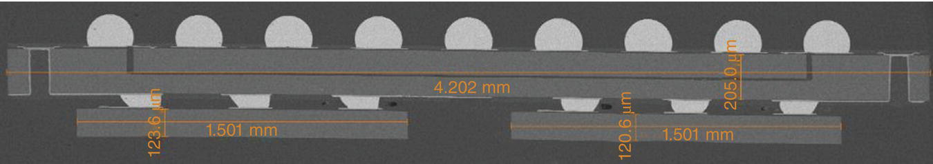
Figure 8.10 Cross‐sectional view of a 3D eSiFO package.
As listed in Table 8.3, electrical tests for daisy chains of 21 3D packages proved that 3D eSiFO package has good electrical connection. Future work for large package, fine‐pitch RDL, and high density TSV will be studied, and reliability evaluation will also be carried out.
Table 8.3 Electrical test results.
| Number of units | Chains per unit | Resistance(Ω) of each chain | Results |
| 21 | 18 | <2.5 | Passed |
8.6 Manufacturing Format and Scalability
Both 8 and 12 in. processes have been developed for eSiFO technology. It will remain at 12 in. wafer manufacturing format since 12 in. silicon wafers are readily available and provide more scale than 8 in. wafers.
The limitation for eSiFO may be the package size. Package sizes larger than 15 mm × 15 mm would have a large CTE mismatch between package and PCB, which may cause failure during TC reliability testing.
8.7 Package Performance
Thermal simulation was used to compare the thermal performance of eSiFO and a type of FO‐WLP called eWLB. In the simulation, the heat dissipation of the chip was assumed to be 3 W, and the package size was fixed as 6 mm × 6 mm × 0.45 mm with an embedded die 100 μm thick. Simulation results under natural convection are shown in Figure 8.11. It can be found that the thermal resistance of both eSiFO and eWLB packages would decrease as the die size increases. Furthermore, thermal resistance of eSiFO is lower than that of eWLB package by 5–40% in all die sizes. This means that the eSiFO package offers significant advantages in thermal performance.

Figure 8.11 Thermal comparison between eSiFO and eWLB package: (a) thermal resistance and (b) temperature distributions for the 4 mm × 4 mm die.
As a wafer‐level package, eSiFO enables short electrical paths from die out to package, and using high‐resistance silicon as the silicon carrier can further improve electrical performance for low loss waveguide transmission. To prove this, a 3D full wave electromagnetic (EM) simulation of package to board transition was conducted from DC to 80 GHz. A coplanar waveguide (CPW) structure of the package side and a substrate integrated waveguide (SIW) structure of the PCB side were chosen to provide low loss and negligible radiation advantages for millimeter‐wave applications [10]. Similarly, high‐resistance silicon was chosen in this simulation. An EM numerical model and simulated S parameter results with/without compensation are shown in Figure 8.12. It is found that after impedance matching, eSiFO can provide ultrawide band at 20 dB return loss and 0.5 dB insertion loss from DC up to 60 GHz. In addition, through transmission line compensation at 77 GHz for automotive radar applications, an absolute bandwidth up to 6 GHz can be realized by eSiFO. The results indicate that eSiFO is qualified for packaging highly integrated millimeter‐wave devices.

Figure 8.12 Electromagnetic simulation of eSiFO package to board transition: (a) EM numerical model and (b) S parameter results.
8.8 Robustness and Reliability Data
Both package‐level and BLR tests have been performed for eSiFO. The results showed that the eSiFO package has a strong robustness.
For package‐level reliability, a 3.9 mm × 3.9 mm package with a body thickness of 350 μm was used. The JEDEC reliability test specifications and conditions are shown in Table 8.4. Prior to the reliability tests, preconditioning was performed to simulate the effects of board assembly on moisturized packaging. The samples were first baked at 125 °C for 24 hours to remove the moisture inside the package and then soaked at 30 °C under 60% relative humidity (RH) for 192 hours. Last, the samples were reflowed at 260 °C for three times. Temperature cycling condition B (TC‐B) test (−55 to 125 °C) up to 1000 cycles, temperature humidity storage (THS) test at 85 °C under 85% RH for 1008 hours, and highly accelerated stress test (HAST) at 110 °C under 85% RH for 264 hours were conducted for reliability evaluation. For each condition of preliminary research, 21 samples were used. According to electrical test results, all the samples passed the reliability tests, as shown in Table 8.4.
Table 8.4 Package‐level reliability test results.
| Reliability test | JEDEC specification | Test condition | Results |
| Preconditioning | JEDECJ‐STD‐020D | 125 °C, 30 °C/60% RH, 3 × reflow | Passed |
| Temperature humidity storage (THS) | JESD22‐A101 | 85 °C/85% RH | Passed |
| Temperature cycling (TC) | JESD22‐A104 | −55/125 °C | Passed |
| Unbiased highly accelerated stress test (HAST) | JESD22‐A118 | 110 °C/85% RH | Passed |
For BLR, a test vehicle of a 3 mm × 3 mm package with a single 1.4 mm × 1.4 mm embedded die was designed, manufactured, and mounted on a board [11]. Several electrical measurement structures, such as daisy chains and single bump resistance measurement, were built in the test vehicle. Four daisy chains with 24 pads were designed in one package, and there were 17 samples in one test board. A typical commercial PCB with 1 mm thickness was chosen for the test board, and two‐layer copper traces with test ports were designed to connect the daisy chains to the board. The designed eSiFO test vehicle and the corresponding mounted board are shown in Figure 8.13. A cumulative distribution function is used to characterize the varied electric resistance of the eSiFO package‐PCB daisy chain loop, and the criterion of failure is that the resistance value exceeds 10% of the average value of the samples. Samples with different package thickness (150, 250, 470 μm) and die thickness (70, 100 μm) were subjected to a board‐level thermal cycling test (−40 to 125 °C). All 68 test samples with underfill passed 1000 cycles. The cumulative percentage of daisy chain electric resistances under TC test is shown in Figure 8.14. It is found that even after TC treatment of 1000 cycles, the average resistance change rate is less than 1%, which indicates that the reliability of the eSiFO package can meet the majority of application requirements.

Figure 8.13 .Test vehicles for board‐level reliability: (a) the designed eSiFO test vehicle and (b) the corresponding mounted board.

Figure 8.14 .Cumulative percentage of daisy chain electric resistances under board‐level temperature cycling test.
8.9 Applications and Markets
The application of eSiFO is similar to eWLB, which can be used to package high performance ASIC (application‐specific integrated circuit), mobile BB/APE (baseband modem/application processor engine), PMU (power management unit), RF transceiver, audio/video codec, sensors, and other multi‐chip and SiP modules. Since ultrathin and ultrasmall packages and SiP integration can be achieved with high yield [9], eSiFO is particularly suitable for the markets of consumer electronics and wearable electronics. For areas with high reliability requirements, such as automotive, medical electronics, and aerospace, some proposed solutions are still in progress. Recently, RF transceiver and driver modules using eSiFO have been in volume production. ASIC, PMU, and sensors using eSiFO are also under development. In the near future, large die packages like APE and ASIC using 3D eSiFO will be also developed.
Acknowledgment
The author would like to thank Dr. Shuying Ma, Dr. Chengqian Wan, Mr. Cheng Chen, Mr. Min Xiang, Ms. Jiao Wang, Mr. Weidong Liu, and other colleagues for the paper preparation and technology development. The support by ASM Pacific Technology, AMEC, and NMC Ltd. for process development was appreciated.
References
- 1 Lau, J.H., Fan, N., and Ming, L. (2016). Design, material, process, and equipment of embedded fan‐out wafer/panel‐level packaging. Chip Scale Review May/June: 38–44.
- 2 Yu D. (2015). Embedded silicon fan‐out package and the method of forming the same. Chinese Patent 201510486674.1, filed 11 August 2015.
- 3 Chong, S.C., Chong, S.C., Wee, D.H.S. et al. (2013). Development of package‐on‐package using embedded wafer‐level package approach. IEEE Transactions on Components, Packaging and Manufacturing Technology 3 (10): 1654–1662.
- 4 Lin, Y., Kang, C., Chua, L. et al. (June 2016). Advanced 3D eWLB‐PoP (embedded wafer level ball grid array‐package on package) technology. In: Proceedings of the 66th Electronic Components and Technology Conference (ECTC), 1772–1777. IEEE Press.
- 5 Huemoeller, R. and Zwenger, C. (2015). Silicon wafer integrated fan‐out technology. Chip Scale Review 19 (2): 10–13.
- 6 Yu, D., Huang, Z., Xiao, Z. et al. (June 2017). Embedded Si fan out: a low cost wafer level packaging technology without molding and de‐bonding processes. In: Proceedings of the 67thElectronic Components and Technology Conference (ECTC), 28–36. IEEE Press.
- 7 Dixit, P. and Miao, J. (2006). Effect of SF6 flow rate on the etched surface profile and bottom grass formation in deep reactive ion etching process. Journal of Physics: Conference Series 34 (1): 577–582.
- 8 Tseng, C.‐F., Liu, C.‐S., Wu, C.‐H., and Yu, D. (June 2016). InFO (wafer level integrated fan‐out) technology. In: Proceedings of the 66th Electronic Components and Technology Conference (ECTC), 1–6. IEEE Press.
- 9 Ma, S., Wang, J., Zhen, F. et al. (2018). Embedded silicon fan‐out (eSiFO): a promising wafer level packaging technology for multi‐chip and 3D system integration. Proceedings of the 68th ElectronicComponents and Technology Conference (ECTC).
- 10 Lee, S., Jung, S., and Lee, H.‐Y. (2008). Ultra‐wideband CPW‐to‐substrate integrated waveguide transition using an elevated‐CPW section. IEEE Microwave and Wireless Components Letters 18 (11): 746–748.
- 11 Cheng, C., Wang, T., Yu, D., et al. (2018). Reliability of ultra‐thin embedded silicon fan‐out (eSiFO) package directly assembled on PCB for mobile applications. Proceedings of the 68th Electronic Components and Technology Conference (ECTC).