
14
Advanced Dielectric Materials (Polyimides and Polybenzoxazoles) for Fan‐Out Wafer‐Level Packaging (FO‐WLP)
T. Enomoto, J.I. Matthews, and T. Motobe
HDMicroSystems
14.1 Introduction
This chapter provides an overview of advanced dielectric materials developed by HD MicroSystems (HDM) that are based on polyimide (PI) and polybenzoxazole (PBO) technologies and that are targeted for use as redistribution layers (RDL) in fan‐out wafer‐level package (FO‐WLP) applications where lithographic and reliability performances are important requirements. The PI/PBO dielectric materials are supplied in liquid form and, as such, are typically applied onto reconstituted wafers using standard spin‐coating processes that include spin coating, soft baking, exposure, development, and final cure.
14.2 Brief History of PI/PBO‐Based Materials in Semiconductor Applications
The first PI products for semiconductor applications were introduced in the early 1970s for use as stress buffers or passivation layers on integrated circuits as well as interlayer dielectrics in high density interconnects on multi‐chip modules. These products, later termed non‐photo‐definable PI (non‐PDPI), were based on polyamic acids (PI precursors) synthesized by reacting dianhydrides with diamines dissolved in a suitable solvent such as N‐methyl pyrrolidone (NMP) and where the dianhydride and diamine were chosen for end‐use performance [1]. These materials were typically processed on a silicon wafer by spin coating, soft baking, and patterning using a conventional photoresist or equivalent process and then cured at temperatures >350 °C to produce the PI polymer (see Figure 14.1).

Figure 14.1 Conversion of polyamic acid to polyimide.
It should be noted that some commercial non‐PDPI materials are not self‐priming (no adhesion promoter present in the formulation), which would mean that an additional step is first required to prime the silicon wafer with an adhesion promoter (typically aminosilane‐based materials diluted in a suitable solvent) to achieve optimum adhesion of the PI to the silicon wafer.
In order to simplify the process and subsequently reduce costs, photo‐definable polyimides (PDPI) were developed in the late 1980s to reduce the number of process steps by eliminating the need to use photoresist. It should also be noted that PDPIs were generally self‐priming, which further reduced the number of process steps. The first PDPIs to be commercialized were negative‐acting, solvent‐developable PI (PI‐Gen1) that, during the exposure step (i‐line or broadband), utilized chain polymerization using radical‐generating photoinitiators to cross‐link acrylate groups present on the polymer backbone (in the form of an ester or an ionic salt) as well as monomers in the formulation [2]. This resulted in the exposed area being relatively insoluble to the developer solution so that only the unexposed areas were removed during development (termed negative acting). The remaining pattern was then cured at temperatures >350 °C to produce the PI film.
In the late 1990s, positive‐acting, aqueous‐developable materials were introduced for additional cost and environmental benefits as well as improved resolution [3–5]. These materials were based on either PI or PBO precursor polymers containing phenolic or acid moieties that provided solubility to alkaline developers such as 2.38% tetramethylammonium hydroxide (TMAH). Patterning was obtained by using diazonaphthoquinone (DNQ) photoacid generators to provide contrast during the exposure and development steps. In the unexposed form, the DNQ interacts with phenolic moieties on the backbone precursor to reduce the dissolution rate [6]. However, on exposure to UV light energy (i‐line or broadband), the DNQ undergoes a Wolff rearrangement to form indene carboxylic acid (ICA) that increases both the dissolution rate and contrast during development (termed positive acting) [7]. The remaining unexposed pattern is then cured at temperatures >300 °C to produce either the PBO or PI film (see Figure 14.2).

Figure 14.2 Positive‐acting PI and PBO.
It should be noted that positive‐acting, aqueous‐developable products based on PBO precursors (PBO‐Gen1) tend to be more widely used as compared with those based on PI precursors. There are no overriding performance differences between the two polymer types although it should be noted that hydroxyl groups on the PBO precursor that allow solubility during development are removed after cure, which can result in a lower moisture uptake (see Figure 14.2). With PI precursors, the hydroxyl or acid moieties that provide solubility during development and that remain on the polymer backbone after development can be reduced by reaction with a suitable thermal cross‐linker during the curing process to improve end‐use properties. Formulation optimization is required to avoid reduction in mechanical properties such as % elongation due to excessive cross‐linking.
As a general comparison, positive‐acting systems have the advantage of resolving smaller via diameters, while negative‐acting systems have more flexibility with respect to processing higher film thicknesses. This is due to the fact that positive‐acting systems using DNQ photoacid generators typically have very high UV light absorption (optical densities >4) at i‐line or broadband wavelengths and are bleached when the DNQ is converted to the ICA, allowing the light to penetrate down into the film during the exposure process. While this can provide more control on resolution, it can be a challenge for thicker films that would require higher exposure energies, resulting in more sloping sidewalls. With negative‐acting systems, the optical density is lower (typically 0.4–0.5) and can be readjusted for thicker films by optimizing the concentration of the photoinitiators to maximize resolution while maintaining an acceptable balance between delamination (in exposed areas) and residue formation (in unexposed areas) [8].
14.3 Dielectric Challenges in FO‐WLP Applications
It is well known that dielectrics based on PI and PBO technologies, due to their proven end‐use performance when cured at temperatures >300 °C, are widely used as RDL in fan‐in wafer‐level packaging (WLP), flip‐chip chip‐scale packaging (FCCSP), and other applications to relocate I/O connections and reduce stress as well as allowing die stacking. However, for FO‐WLP applications, as the reconstitution process requires the use of a molding compound that has a Tg around 150–170 °C, new PI and PBO materials are needed that can be cured at lower temperatures while still meeting process, end‐use, and reliability requirements in FO‐WLP applications [9, 10]. The challenges for dielectric materials in FO‐WLP applications based on PI and PBO polymer technologies are listed as follows:
- Low temperature cure. As indicated above, for FO‐WLP applications, the molding compound used in the reconstitution process typically has a Tg around 150–170 °C, which subsequently limits the cure temperature used for processing dielectrics. While the current cure temperature range for PI or PBO materials in FO‐WLP applications is 200–230 °C, <200 °C will be required for lower warpage and higher yield in next‐generation FO‐WLP devices designed to include memory chips, and, in this respect, PI and PBO materials need to be further redesigned for lower cure temperatures (<200 °C) for next‐generation FO‐WLP applications [11–16].
- Cured film thickness. Cured film thicknesses varying from 4 to 20 μm are required depending on the copper (Cu) track thickness, which can influence both electrical performance as well as reliability at the solder joint.
- High resolution. As devices get smaller and the number of I/O connections continues to increase, lithographic performance is becoming more stringent regarding resolution, with the current target being 10 μm via openings. For future FO‐WLP devices, this could be reduced further to 5 μm. The challenges with a positive‐acting, aqueous‐developable PBO are to increase both contrast for improved resolution and thickness range while avoiding delamination (see Figure 14.3a). With a negative‐acting, solvent‐developable PI, the challenge is to reduce residue (footing) due to scattered light at fine resolutions (see Figure 14.3b).
- Sidewall shape. Regarding sidewall shape, there is no specific target for the slope angle, although too steep an angle (like a cliff) should be avoided to prevent concentration of stress from the solder bump on the top corner edge of the sidewall and also to produce a more even distribution of Cu during the plating process. In this respect, a smooth profile with no crowning at the top edge of the sidewall and a sidewall angle of 70–80° to the substrate surface is preferred.
- Deep gap formability. For some applications, deep gap formability is required to develop pre‐baked films up to 25 μm to open scribe lines when processing multiple RDL (see Figure 14.4).
- Elongation. A high % elongation is required to enhance crack resistance (see Figure 14.5) between Cu and the dielectric interface and also between dielectric layers during temperature cycle test (TCT) and pressure cooker testing (PCT). Typical test conditions for TCT and PCT are given in Table 14.1.
- Chemical resistance. High chemical resistance to selected chemicals (resist strippers, etchants, fluxes) used in both the RDL and bumping process that can result in delamination (see Figure 14.6) provides a wider process window for the PI and PBO dielectrics and subsequently avoids performance issues during reliability testing.
- Adhesion to Cu. The adhesion between Cu and the dielectric needs to be strong enough to avoid any delamination occurring at the Cu and dielectric interface (see Figure 14.7) that can act as the origin of crack propagation during PCT and TCT (see Table 14.1 for typical test conditions). The adhesion strength is typically measured either using the stud pull test or through visual examination under a microscope for delamination or cracking.
- Insulation. In order to maintain insulation between Cu tracks with finer line and space (L/S) patterns down to 5/5 μm or even 2/2 μm L/S, no short circuiting as observed by changes in electrical resistance should occur during biased highly accelerated stress testing (bHAST). In addition, any dendrite formation, corrosion, or delamination as checked for through visual examination (see Figure 14.8) under a microscope should be avoided. The test conditions for the bHAST are given in Table 14.1.

Figure 14.3 Defects in fine patterning. (a) Positive acting PBO. (b) Negative acting PI.

Figure 14.4 Deep gap formability for multilayer structures.

Figure 14.5 Cracking at Cu pad area after TCT.
Table 14.1 PI and PBO dielectric challenges for FO‐WLP applications.
| Challenge | Application | Target specification |
| 1. Cure temperature | Processing | <200 °C |
| 2. Cured film thickness | Processing | >15 μm cured film |
| 3. Resolution | Processing | <10 μm via opening |
| 4. Sidewall shape | Processing | 70–80° acute angle to the substrate surface |
| 5. Deep gap formability | Processing | Develops ~25 μm pre‐bake films with no residues |
| 6. Elongation | End‐use properties | Pass reliability testing (>40% at ambient)
|
| 7. Chemical resistance | End‐use properties | Resistance to downstream chemicals used in Fab
|
| 8. Adhesion to Cu | Reliability testing | No delamination at stud pull test after:
|
| 9. Insulation | Reliability testing | No short circuit with 5/5 or 2/2 μm L/S after:
|

Figure 14.6 Delamination after immersion in resist stripper.

Figure 14.7 Crack propagation from delamination at the Cu surface.

Figure 14.8 Short circuit after bHAST (20 μm space pattern).
An overview of the main challenges is given in Table 14.1.
In order to meet these challenges for next‐generation FO‐WLP applications, a new generation of positive‐acting, aqueous‐developable and negative‐acting, solvent‐developable materials has been developed that will be outlined in the next section.
14.4 HDM Material Sets for FO‐WLP
As indicated previously, PI‐Gen1 and PBO‐Gen1 were among the first photo‐definable PI and PBO materials, respectively, to be introduced as dielectrics for semiconductor applications that are still widely accepted for use as stress buffers, RDL for WLP, FCCSP, and others where both materials are typically cured at >300 °C for optimum end‐use and reliability properties. It should be noted that the high cure temperatures used in the processing of PI‐Gen1 and PBO‐Gen1, in addition to producing complete ring closure of the PI/PBO precursors, also resulted in the emission of the photo‐package and other additives to varying levels to allow the backbone polymer to achieve end‐use properties similar to non‐PDPI materials.
In order to address the need to reduce cure temperatures for FO‐WLP and other semiconductor packaging applications, the development concept as outlined in Figure 14.9 was to redesign the backbone polymers for lower temperature cure as well as introducing novel photoinitiators, cross‐linkers, and additives to assist in addressing the challenges described in the previous section.

Figure 14.9 Design concept of a low temperature cure material.
The correlation between the performance challenges and the types of materials used to meet those challenges are given in Figure 14.10. From a formulation perspective, it can be seen that there is significant interdependency between raw material choice and the subsequent influence on processing, end‐use properties, and reliability performance.

Figure 14.10 Correlation between challenges and materials.
This development program resulted in a number of materials being introduced where the cure temperature was reduced below 300 °C and where PBO‐Gen2 was the first product introduced by HDM that could be cured at 200 °C (see Table 14.2).
Table 14.2 Overview of PI/PBO material sets.
| Material | PI‐Gen1 | PI‐Gen2 | PBO‐Gen1 | PBO‐Gen2 | PBO‐Gen3 |
| Tone | Negative | Negative | Positive | Positive | Positive |
| Development | Solvent | Solvent | Aqueous | Aqueous | Aqueous |
| Cure | High temp | Low temp | High temp | Low temp | Low temp |
| Cure (°C) | 350–390 | 175–250 | 320–350 | 200–250 | 175–250 |
In order to reduce further the cure temperature to <200 °C to address the current challenges for next‐generation FO‐WLP applications described above, further development work has resulted in two new low temperature cure materials:
- PBO‐Gen3 (positive‐acting, aqueous‐developable PBO)
- PI‐Gen2 (negative‐acting, solvent‐developable PI)
Both materials have also been developed in solvents other than NMP. Process and end‐use reliability data for both PBO‐Gen3 (with PBO‐Gen2 used as a reference) and PI‐Gen2 are outlined in detail in the following sections.
14.5 PBO‐Gen3 (Positive‐Acting, Aqueous‐Developable Material)
This section details the process flow, lithography, material properties, and reliability performance that have been generated for PBO‐Gen3 to date and where PBO‐Gen2 is used as a reference. As indicated in a previous section, PBO‐Gen2 was the first product introduced by HDM that could be cured at 200 °C and where the design concepts used in the development of PBO‐Gen2 involved developing a more flexible polymer backbone to facilitate cyclization at lower cure temperatures, introducing selected cross‐linkers for improved thermal properties as well as additives to address adhesion and copper compatibility. However, to meet the challenges discussed previously with respect to both process and reliability requirements for FO‐WLP applications, the following performance improvements to the PBO‐Gen2 formulation were undertaken that resulted in the development of PBO‐Gen3:
- An alternative photo‐package was selected to improve lithographic performance.
- A novel cross‐linker was introduced to enhance chemical resistance, moisture resistance, and adhesion to Cu.
- A new additive was added to improve lithographic performance on Cu as well as adhesion to Cu at low cure temperatures.
14.6 PBO‐Gen3 Process Flow
The process flow for PBO‐Gen3 is outlined in Table 14.3 where spin speeds, pre‐bake conditions, exposure energies, development times, and curing conditions are given for 5, 7, and 10 μm cured films together with thicknesses after pre‐bake, development, and cure.
Table 14.3 PBO‐Gen3 process flow.
| Condition | ||||||
| Process | Unit | 5 μm | 7 μm | 10 μm | Remarks | |
| Coating | Pre | rpm/s | 1000/5 | |||
| Main | 3000/30 | 2000/30 | 1200/30 | |||
| Pre‐bake | °C/s | 110/180 | Hot plate | |||
| Thickness after pre‐bake | μm | 8.1 | 11.2 | 16.4 | ||
| Exposure dose (i‐line) | mJ/cm2 | 160 | 220 | 300 | ||
| Development | s | 30 × 2 | 40 × 2 | 55 × 2 | 2.38% TMAH | |
| Film thickness after dev. | μm | 6.2 | 8.7 | 12.1 | ||
| Cure profile | — | Step 1: ramp up to 100 °C (10 °C/min) | Under N2 | |||
| Step 2: hold for 30 min | ||||||
| Step 3: ramp up to 175–250 °C (10 °C/min) | ||||||
| Step 4: hold for 120 min | ||||||
| Film thickness after cure | μm | 5.1 | 7.1 | 10.3 | ||
Setting up the PBO‐Gen3 process requires balancing coating thickness, pre‐bake, exposure, development, and cure conditions to provide the desired final film resolution, cured film thickness, and film properties. It should be noted that the process conditions outlined in Table 14.3 can vary depending on equipment used and clean room conditions. Please note some general points regarding the spin‐coating process:
- The spin‐coating speed generally controls the range of cured coating thicknesses although the final coating thickness can also be influenced to a lesser extent through surface topography, processing equipment, and clean room environment. With current Cu track thicknesses in FO‐WLP applications typically being around 5 μm, acceptable coverage of the Cu track can be achieved with a 7 μm cured film thickness.
- The pre‐bake step removes the bulk of the solvent, resulting in a film that is “dry to the touch,” which can be handled in subsequent processes.
- Both i‐line (365 nm) and broadband steppers can be used for the exposure process.
- The development process (typically puddle) removes all of the exposed film as well as some unexposed film on the wafer. The ratio of the remaining unexposed film thickness to the initial pre‐baked film thickness is known as the percentage film retention (% FR) after development.
- Curing is typically performed as a batch process using programmable ovens or furnaces under a nitrogen atmosphere (oxygen concentration < 100 ppm).
- In setting up the process for PBO‐Gen3, based on the conditions outlined in Table 14.3, the pre‐bake and development conditions are first adjusted to a predetermined % FR after development (see Table 14.4). The exposure energy is then optimized (avoiding any residue formation due to underexposure or film lifting due to overexposure) for resolution and pattern profile.
Table 14.4 Film retention (FR) comparison between PBO‐Gen3 and PBO‐Gen2.
| PBO‐Gen2 | PBO‐Gen3 | |||
| Item | Unit | 200 °C/1 h | 175 °C/2 h | 200 °C/2 h |
| Thickness after pre‐bake | μm | 15.8 | 15.8 | 16.4 |
| Thickness after development | μm | 12.3 | 11.9 | 12.1 |
| Thickness after cure | μm | 10.3 | 10.0 | 10.3 |
| % FR after development | % | 78 | 75 | 74 |
| % FR after cure | % | 84 | 84 | 85 |
| Overall % FR | % | 65 | 63 | 63 |
Regarding the processing of PBO‐Gen3 and PBO‐Gen 2, both materials, as indicated in Table 14.4, produce similar film thicknesses after pre‐bake, development, and cure that are further reflected in the % FR after development (74–78%), % FR after cure (84–85%), and overall % FR (63–65%).
14.7 PBO‐Gen3 Lithography
14.7.1 PBO‐Gen3 Resolution
Using the process conditions given in Table 14.3, high resolution down to 2 μm L/S and 2 μm via openings are obtained with PBO‐Gen3 on both Si and Cu with a 7 μm cured film thickness (see Figure 14.11) that also resulted in a smooth sidewall with no crowning of the dielectric being observed at the interface of the top edge and top surface of the sidewall (see Figure 14.12). Regarding the sidewall slope, too steep an angle is unsuitable due to stress concentration at the edge of the pattern, which can also reduce copper plating distribution, while too shallow an angle is not preferable for fine patterning. In this respect, the sidewall angle of 70–80° that was obtained is an acceptable compromise.

Figure 14.11 PBO‐Gen3 resolution on Si and Cu (7 μm thickness after cure). (a) and (c) show L/S patterns on Si and Cu, respectively. (b) shows a via pattern on Si.

Figure 14.12 PBO‐Gen3 lithographic performance (cross‐sectional 7 μm thickness after cure).
14.7.2 PBO‐Gen3 Thick Film Formability
A higher viscosity version of PBO‐Gen3 was developed for thick film formability where >15 μm cured film thicknesses are required. The process flow for cured film thicknesses ranging from 15 to 20 μm is outlined in Table 14.5.
Table 14.5 PBO‐Gen3 (high viscosity version) process flow for thick film formability.
| Condition | ||||||
| Process | Unit | 15 μm | 17.5 μm | 20 μm | Remarks | |
| Coating | Pre | rpm/s | 1000/5 | |||
| Main | 1800/30 | 1500/30 | 1200/30 | |||
| Pre‐bake | °C/s | 80/180 + 110/270 | Hot plate | |||
| Thickness after pre‐bake | μm | 25.8 | 29.5 | 34.2 | ||
| Exposure dose (i‐line) | mJ/cm2 | 560 | 640 | 820 | ||
| Development | s | 43 × 4 | 47 × 4 | 55 × 4 | 2.38% TMAH | |
| Film thickness after dev. | μm | 18.6 | 21.4 | 24.4 | ||
| Cure profile | — | Step 1: ramp up to 100 °C (10 °C/min) | Under N2 | |||
| Step 2: hold for 30 min | ||||||
| Step 3: ramp up to 175–250 °C (10 °C/min) | ||||||
| Step 4: hold for 120 min | ||||||
| Film thickness after cure | μm | 15.4 | 17.7 | 20.2 | ||
As compared with the standard PBO‐Gen3 process outlined in Table 14.3, the process for the higher viscosity version requires:
- Lower spin speed to achieve the desired film thickness.
- Two‐step pre‐bake to achieve a “dry to the touch” film.
- Higher exposure energies to allow exposure through the whole thickness of the thicker dried film.
- Longer development times to develop out the thicker film.
- No change in the cure process.
As indicated in Table 14.6, the higher viscosity version of PBO‐Gen3 also has high resolution (2–3 μm with both via and L/S), high aspect ratio, and smooth sidewalls with no crowning with cured film thicknesses up to 15 μm (a 10 μm via opening with a 20 μm cured film thickness is shown in Figure 14.13). This is in comparison with PBO‐Gen2 that has lower resolution at higher film thicknesses and still requires higher exposure energies.
Table 14.6 PBO‐Gen3 and PBO‐Gen2 thick film patterning capability.
| Sample | Thickness after PB (μm) | Exposure dose (mJ/cm2) | Thickness after dev. (μm) | % FR after dev. | Thickness after cure (μm) | Resolution via and L/S (μm) | Aspect ratioa |
| PBO‐Gen2 | 11.2 | 230 | 8.5 | 75.9 | 7.3 | 2 | >3.5 |
| 19.8 | 1040 | 15.2 | 76.8 | 12.2 | 10–15 | 1 | |
| PBO‐Gen3 | 11.4 | 180 | 8.5 | 74.6 | 7.2 | 2 | >3.5 |
| 20.3 | 500 | 15.6 | 76.8 | 13.1 | 3 | >4 | |
| 27.4 | 640 | 19.9 | 72.6 | 15.6 | 3 | >5 |
aAspect ratio = thickness after cure/resolution.

Figure 14.13 PBO‐Gen3 thick film formability.
14.7.3 PBO‐Gen3 Deep Gap Formability
PBO‐Gen3 can be also used for deep gap formability applications to open scribe lines after processing multiple RDL (see Figure 14.4) and where no residues were observed after exposure and development with a 25 μm pre‐baked thickness film as compared with PBO‐Gen2 where residues were found after development (see Figure 14.14). It should be noted that, as outlined in Table 14.5, higher exposure energies and development times are required during processing of pre‐bake thicknesses up to 25 μm.

Figure 14.14 Deep gap formability performance.
14.8 PBO‐Gen3 Material Properties
Mechanical and thermal end‐use properties as well as residual stress are measured to provide performance indicators for dielectric materials in downstream processes used in the manufacture of FO‐WLP devices as well over the lifetime of the semiconductor device. Mechanical properties (modulus, tensile strength, and % elongation) are measured as freestanding films on a tensile tester using the following test procedure:
- The test material is processed on 6″ Si wafers as follows:
- Spin coat and pre‐bake to target a 10 μm cured film thickness.
- Expose (1000 mJ cm−2) using a BB stepper through a glass mask designed with 10 mm wide rectangular strip patterns.
- Develop (puddle) in 2.38% TMAH to target 75% FR.
- Cure in a furnace under a nitrogen atmosphere at the desired temperature for two hours. The wafers with the cured test material are immersed into a 4.9% HF aqueous solution to release the films from the Si wafer and then washed with distilled water and dried in air.
- The cured freestanding films (dimensions: thickness 10 μm, width 10 mm, length 70–100 mm) are then mounted onto a tensile tester (chuck distance 20 mm, pull speed 5 mm min−1) at ambient temperature and tested for mechanical properties.
The mechanical and thermal end‐use properties as well as residual stress for PBO‐Gen3 and PBO‐Gen2 are given in Table 14.7. From the data, it can be seen that, due to the combination of appropriate cross‐linkers with the base polymer that produces a robust and ductile 3D cross‐linking structure, both PBO‐Gen3 and PBO‐Gen2 achieve acceptable end‐use properties, resulting in a wide cure temperature margin over the cure temperature range of 175–250 °C.
Table 14.7 PBO‐Gen3 and PBO‐Gen2 cured film properties.
| Item | Unit | PBO‐Gen2 | PBO‐Gen3 | ||||||
| Cure temp. | °C | 175 | 200 | 225 | 250 | 175 | 200 | 225 | 250 |
| Tensile strength | MPa | 170 | 170 | 170 | 170 | 160 | 150 | 120 | 120 |
| % Elongation (ave.) | % | 85 | 80 | 80 | 80 | 65 | 70 | 70 | 55 |
| Young’s modulus | GPa | 1.9 | 1.8 | 1.8 | 1.7 | 2.1 | 2.0 | 1.8 | 1.7 |
| T g | °C | 240 | 240 | 245 | 245 | 240 | 245 | 255 | 270 |
| CTE | ×10−6/°C | 80 | 80 | 80 | 80 | 75 | 75 | 80 | 84 |
| Weight loss temp. (5%) | °C | 280 | 310 | 345 | 360 | 300 | 320 | 340 | 365 |
| Residual stress | MPa | 25 | 27 | ||||||
One important point to note is that mechanical properties and in particular % elongation can be linked to performance in TCT, which is conducted to determine the effect of extreme changes in temperature on the overall performance of a device as well as the materials used to manufacture the device. In this respect, the % elongation of both the PBO‐Gen3 and PBO‐Gen2 when measured at ambient temperatures after TCT testing (JESD22‐A104 Condition C) is not significantly changed after 1000 cycles (see Table 14.8).
Table 14.8 Mechanical properties after TCT (−65 °C/15 min to 150 °C/15 min).
| Sample | Cure temp. (°C/2 h) | TCT (cycles) | Tensile strength (MPa) | Elongation (%) | Modulus (GPa) |
| PBO‐Gen2 | 200 | 0 | 125 | 86 | 1.8 |
| 1000 | 141 | 82 | 1.8 | ||
| PBO‐Gen3 | 200 | 0 | 148 | 55 | 2.0 |
| 1000 | 111 | 58 | 2.1 |
However, any brittleness that occurs with organic polymers at low temperatures can result in a drop in % elongation when measured at that low temperature, which can subsequently produce cracks in the dielectric and damage to the copper tracks. This means that high % elongation when measured at low temperature is an important property in ensuring maximum reliability performance.
The effect of measuring % elongation at different temperatures is subsequently shown in Table 14.9 where the % elongation of PBO‐Gen3 and PBO‐Gen2 decreases when measured at −50 °C (limit of the equipment used) as compared with 25 °C. However, the drop in % elongation with PBO‐Gen3 (65% at ambient dropping to 44% at −50 °C) is not as prominent as compared with PBO‐Gen2 (54% at ambient temperature dropping to 16% at −50 °C), which would suggest an improved performance with PBO‐Gen3 as compared with PBO‐Gen2 (see Figure 14.15). From these tests, the main conclusion is that the % elongation of 40–45% obtained with PBO‐Gen3 when measured at −50 °C is ductile enough to provide crack resistance and so avoid performance issues during component and board reliability testing involving TCT (see section on PBO‐Gen3 package reliability performance). These results further indicate that the temperature at which the films are being measured for mechanicals is a critical factor in determining reliability performance.
Table 14.9 Mechanical properties (ambient versus −50 °C).
| Sample | Cure temp. (°C/2 h) | Measurement temp. (°C) | Tensile strength (MPa) | Elongation (%) | Modulus (GPa) |
| PBO‐Gen2 | 200 | 25 | 134 | 54 | 2.6 |
| −50 | 120 | 16 | 2.6 | ||
| PBO‐Gen3 | 200 | 25 | 147 | 65 | 2.7 |
| −50 | 164 | 44 | 2.6 |

Figure 14.15 Mechanical properties. Examples of stress–strain curves (25 vs. −50 °C).
In addition, after PCT, while a slight drop in % elongation (65–60%) and modulus (2.7–2.3 GPa) was observed with PBO‐Gen3 after 168 hours PCT (see Table 14.10), no brittleness was observed due to any interaction with moisture. This is in comparison with PBO‐Gen2 where, after PCT, the cured film was very brittle with a hazy appearance such that mechanical testing could not be conducted on the cured films.
Table 14.10 Mechanical properties after PCT (121 °C/100% RH, 168 h).
| Sample | Cure temp. (°C/2 h) | PCT (hours) | Tensile strength (MPa) | Elongation (%) | Modulus (GPa) |
| PBO‐Gen2 | 200 | 0 | 156 | 73 | 1.9 |
| 168 | No data | ||||
| PBO‐Gen3 | 200 | 0 | 147 | 65 | 2.7 |
| 168 | 149 | 60 | 2.3 | ||
One important point to note is that the % elongation obtained is not an absolute measurement and can vary from one test location to another depending on processing conditions of the cured film to be tested, test equipment, and test procedure. However, when measured side‐by‐side, % elongation data can be used as a guide to performance during reliability testing and where it can be seen that the % elongation of the PBO‐Gen3 is superior to PBO‐Gen2 when measured at −50 °C (see Table 14.9 and Figure 14.15) and after PCT (see Table 14.10).
14.9 PBO‐Gen3 Dielectric Reliability Testing
Reliability testing is undertaken to determine that the dielectric is not degraded in any way during downstream processes that can result in yield losses and also that the performance of the dielectric does not change over the lifetime of the semiconductor device. In this respect, the following tests were conducted on PBO‐Gen3 with PBO‐Gen2 as a reference:
- Adhesion strength to Cu and PBO/PBO after PCT.
- Resistance to chemicals used in downstream processing.
- bHAST.
14.9.1 PBO‐Gen3 Adhesion After PCT
In the FO‐WLP device, delamination at the interface between the dielectric and either the Cu track or another layer of dielectric can induce cracking of both the dielectric material and the Cu track in the RDL layers. In addition, delamination can also induce electrochemical copper migration between Cu tracks in the presence of moisture as Cu ions can easily be generated from the surface of the anode, subsequently move freely through the moisture, and be immediately converted to Cu at the cathode. This is a typical propagation mechanism for Cu dendrite formation where moisture can act as a medium for accelerating Cu migration. Therefore, good adhesion of the dielectric to Cu as well as between two dielectric layers is important for package reliability.
The PCT was originally adopted to shorten the time to failure of a semiconductor chip in a molded package due to the erosion of Al lines. Once delamination between the molding compound and the chip occurs due to degradation of the molding compound under high humidity conditions, moisture that penetrates into the molded package collects at the delamination site and accelerates the erosion of the Al lines. In this respect, PCT treatment was found to be a good method to evaluate the adhesion performance of molding compounds and has subsequently been used to accelerate the adhesion performance of organic dielectric materials in electronic applications.
The adhesion strength of both PBO‐Gen3 and PBO‐Gen2 to Cu and PBO/PBO was measured using a stud pull test before and after PCT (121 °C/100% RH, 300 hours, JESD22‐A102). The samples used to test for PBO/Cu adhesion were prepared as follows:
- The stud pin with an epoxy adhesive is fixed to a cured test film processed on a silicon wafer electroplated with Cu. The epoxy adhesive is then cured at 120 °C for one hour.
- The test specimen is placed on the stud pull tester, and the stud pin is gradually pulled down vertically until breakage occurs. If breakage of the epoxy adhesive occurs, the adhesion strength of the dielectric to Cu is higher than the epoxy cohesion strength, and this breakage mode indicates good adhesion performance to Cu. In contrast, if delamination at the interface between Cu and the cured dielectric film occurs, the adhesion strength to Cu is lower than the epoxy cohesion strength, and this breakage mode is unacceptable.
- The same test procedure is then conducted with the cured film after PCT treatment in order to evaluate the adhesion performance before and after PCT treatment.
For PBO/PBO adhesion testing, the test dielectric is first processed to cure (200 °C/2 h) on a silicon wafer electroplated with Cu and an additional layer of the test dielectric processed to cure (200 °C/2 h) over the first cured film. The stud pull test is then conducted using the procedure described above. It should be noted that the limitation of using the stud pull test is that the actual adhesion strength above the epoxy cohesion strength cannot be measured. In addition, adhesion can only be measured at ambient temp. and cannot be measured at high temperatures that simulate reflow conditions.
It can be seen from Figures 14.16 and 14.17 that PBO‐Gen3 cured at 175 and 200 °C passed the stud pull test to both Cu and to itself after 300 hours PCT. This is in comparison with PBO‐Gen2 cured at 175 and 200 °C, which failed on Cu after 200–300 hours PCT and PBO/PBO after 300 hours PCT.

Figure 14.16 Adhesion stud pull test results on Cu after PCT.

Figure 14.17 Adhesion stud pull test results on PBO/PBO after PCT.
The adhesion strength of PBO‐Gen3 and PBO‐Gen2 to Cu L/S after PCT was also tested using the following procedure:
- The test dielectric is spin‐coated over the 10 μm Cu L/S, pre‐baked, and cured (200 °C/2 h).
- The coated test sample is then placed in a PCT chamber set to 121 °C/100% RH for 300 hours.
- Cross sections before and after PCT are inspected for delamination using scanning electron microscopy (SEM).
The adhesion results for PBO‐Gen3 and PBO‐Gen2 on 10 μm Cu L/S are shown in Figure 14.18. Although simulation analysis of stress distribution in dielectric layers indicated that the tensile stress is concentrated at the sidewall of the Cu line, which can induce delamination at that point, it should be noted that no delamination was observed with PBO‐Gen3 in contrast to PBO‐Gen2.

Figure 14.18 Cross sections of (a) PBO‐Gen2 and (b) PBO‐Gen3 on a Cu line after PCT.
The improved adhesion performance of PBO‐Gen3 over PBO‐Gen2 on Cu is due to PBO‐Gen3 having improved Cu compatibility and higher interaction with the Cu surface due to the choice and optimization of both cross‐linker as well as additives used in the PBO‐Gen3 formulation to improve adhesion. In addition, as discussed previously, PBO‐Gen3 is more ductile and does not degrade during PCT, which results in higher PBO‐Gen3/PBO‐Gen3 adhesion as compared with PBO‐Gen2 after PCT.
14.9.2 PBO‐Gen3 Chemical Resistance
Chemical resistance to selected chemicals used in the RDL and bumping processes provides a wider process window for PBO and PI dielectrics and subsequently avoids performance issues such as cracking, delamination, and thickness changes during reliability testing. The following chemicals were chosen due to their frequent use in the RDL and reflow process:
- Rework solvent (NMP) used to remove pre‐baked PBO films as well as a cleaner for removing residues.
- Photoresist stripper (Dynastrip 7700, Dynaloy) used to remove photoresist after the Cu plating process.
- Resist cleaner (OK‐73, Tokyo Ohka Kogyo) used to remove any residues remaining after the stripping process.
- Flux (WS‐600, Cookson Electronics) used to remove any oxide on the surface of the solder ball before reflow (WS‐600 is a strong acid that is applied directly to the surface of the dielectric material before reflow).
The test procedure for chemical resistance is as follows:
- Process 7 μm cured films with a 100 μm square pattern on Si wafers.
- Dip the cured film into the selected chemical under the test conditions outlined in Table 14.11.
- Remove the cured film, wash with distilled water, and dry in air at ambient temp.
- Measure thickness of the cured film by a stylus type thickness measurement tool.
- The film thickness change is then estimated by comparing with the initial thickness.
- Conduct a visual check using an optical microscope (100× magnification).
Table 14.11 Chemical resistance of PBO‐Gen2 and PBO‐Gen3.
| Treatment conditions | PBO‐Gen2 | PBO‐Gen3 | ||||
| Chemicals | Temp. (°C) | Time (min) | Check itema, b | 200 °C 1 h |
175 °C 2 h |
200 °C 2 h |
| Rework solvent (NMP) | 25 | 30 | Appearance | Cracking | No change | No change |
| Film thickness change | OK | OK | OK | |||
| Resist stripper (Dynastrip 7700) | 70 | 30 | Appearance | Delamination | No change | No change |
| Film thickness change | OK | OK | OK | |||
| Resist cleaner (OK‐73) | 25 | 60 | Appearance | Cracking | No change | No change |
| Film thickness change | OK | OK | OK | |||
| Flux (WS‐600) | 245 | 1 | Appearance | 25% swelling | No change | No change |
| Film thickness change | OK | OK | OK | |||
a Appearance No change = no cracking, no delamination, and no hazing.
b Film thickness change % change within ±10% is acceptable.
The chemical resistance results are given in Table 14.11 where no changes were observed in either appearance or film thickness of the PBO‐Gen3 even when cured at 175 °C after immersion in the chemicals described above for a given temperature and time. This is in contrast to PBO‐Gen2 that shows delamination and cracking at 200 °C with NMP, Dynastrip 7700, and OK‐73 (see Table 14.11 and Figure 14.19). It should also be noted that no thickness change occurred with PBO‐Gen3 after treatment with WS‐600 flux, while PBO‐Gen2 swelled by 25%.
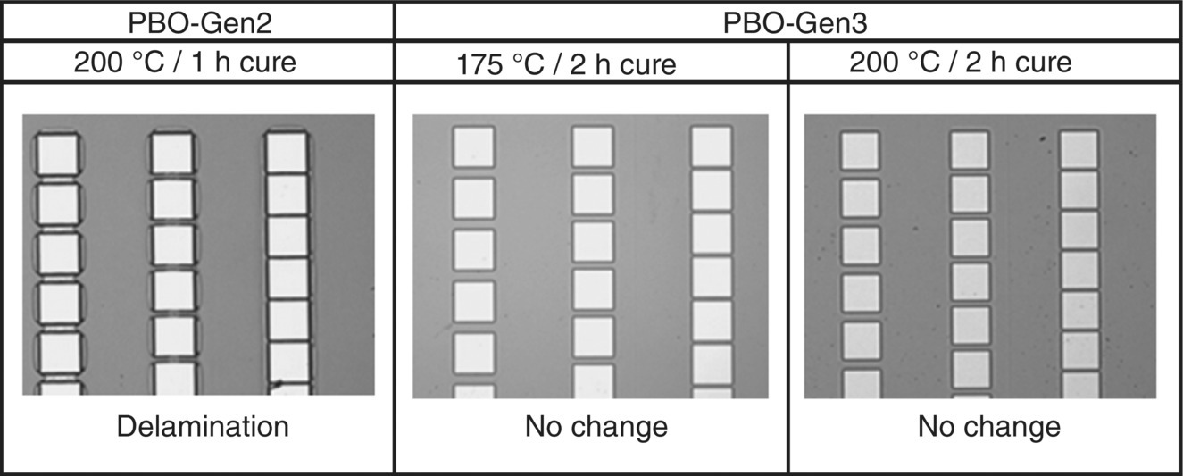
Figure 14.19 PBO‐Gen2 and PBO‐Gen3 appearance (100 μm sq. pattern) after immersion in resist stripper.
14.9.3 PBO‐Gen3 bHAST
bHAST uses temperature, humidity, and bias to accelerate the penetration of moisture through a dielectric, which can cause performance loss or electrical breakdown (JESD22‐A110). For FO‐WLP applications, bHAST is used to determine the insulation reliability of the dielectric between Cu tracks and is becoming more important with the recent trend toward finer L/S designs [17–19].
The test vehicle used for the test was processed in cooperation with the Hitachi Chemical Packaging Solution Center and consists of 5/5 and 2/2 μm Cu L/S processed on PI‐Gen1 (see Figure 14.20). The test procedure is as follows:
- The test dielectric is spin‐coated, pre‐baked, and cured at 200 °C/2 h so as to cover the 5/5 or 2/2 μm L/S Cu comb pattern.
- The anode and cathode of the test sample are connected, respectively, by wires to a migration tester equipped with HAST chamber and monitoring unit.
- The HAST chamber is set to 130 °C and 85% RH.
- DC voltage at 3.3 V is applied constantly, and in situ insulation resistance is monitored during testing.

Figure 14.20 Test vehicle for bHAST.
bHAST results for PBO‐Gen3 indicated that no short circuits, dendrite formation, or delamination was observed with both 5/5 and 2/2 μm Cu L/S after 200 hours (longer than the required standard test time of 168 hours) as well as no change in the insulation resistance (see Figure 14.21). This is in comparison with PBO‐Gen2 that failed bHAST after 200 hours.

Figure 14.21 PBO‐Gen3 insulation resistance during bHAST (130 °C/85% RH/3.3 V, L/S = 5/5 and 2/2 μm).
14.10 PBO‐Gen3 Package Reliability Performance (TCT Testing at Component and Board Level)
The main purpose in conducting dielectric reliability testing at the component level is to define or determine the influence of any degradation of the dielectric materials under severe environmental conditions (moisture, temperature, and bias voltage) on device performance, which has already been discussed in part in a previous section. On the other hand, conducting dielectric reliability tests at the board level is focused more on the mechanical stress around solder joints as well as the durability to the stress induced by CTE mismatches between the device and board.
There are a number of reliability tests that can be conducted at the component and board level that include moisture sensitivity levels (MSL), TCT, high temperature storage (HTS) test, unbiased highly accelerated stress test (uHAST), and the drop test. However, for initial component and board‐level testing, TCT was regarded as the most useful test to provide performance on actual stress produced due to temperature variation [20–22].
The test vehicle used for the TCT was assembled in cooperation with the Hitachi Chemical Packaging Solution Center. The processing of the FO‐WLP test vehicle is shown in Figure 14.22 together with a cross section of the test vehicle in Figure 14.23. Details of the vehicle structure are outlined in Table 14.12.

Figure 14.22 Assembly process of FO‐WLP test vehicle used for reliability testing (12 in. process).

Figure 14.23 Cross section of FO‐WLP test vehicle.
Table 14.12 Specification of FO‐WLP test vehicle.
| Classification | Specification | |
| FO‐WLP | Package size (mm) | 9.6 × 9.6 |
| Package thickness (μm) | 450 | |
| Molding compound | High Tg type (granule, Hitachi Chemical) | |
| Chip size (mm) | 7.3 × 7.3 | |
| Chip thickness (μm) | 400 | |
| First dielectric layer thickness (μm) | 7 | |
| Second dielectric layer thickness (μm) | 7 | |
| Cu line thickness (μm) | 5 | |
| Bump material | Sn‐3.0Ag‐0.5Cu | |
| Bump diameter (μm) | 250 | |
| Bump number | 336 | |
| Bump pitch (μm) | 300 | |
| Substrate | Material | FR‐4 |
| Size (mm) | 17 × 17 | |
| Thickness (mm) | 0.8 | |
| Surface finish | E‐less Ni/Au plating | |
| Underfill | High Tg type (Hitachi Chemical) | |
For the component‐level evaluation, the test vehicle was preconditioned at 85 °C/85% RH for 168 hours followed by 10× N2 reflow at 260 °C and then subjected up to 1000 TCT cycles (−65 °C/15 min ↔ 150 °C/15 min). The test vehicle was visually inspected using an optical microscope for any defects at 200 cycle intervals and no cracking or delamination was observed after 1000 TCT cycles (see Table 14.13).
Table 14.13 PBO‐Gen3 (cured 200 °C/2 h) reliability test results after TCT at component and board level.
| Reliability test result (component level) | Reliability test result (board level) | |
| TCT cycles | Appearance after TCT | Cumulative electrical failure rate (%) |
| 0 | No crack or delamination | 0 |
| 200 | No crack or delamination | 0 |
| 400 | No crack or delamination | 0 |
| 600 | No crack or delamination | 0 |
| 800 | No crack or delamination | 0 |
| 1000 | No crack or delamination | 0 |
For the board‐level evaluation, a one‐time reflow treatment (260 °C max) without moisture soaking was used to mount the test vehicle onto the board and then subjected to 1000 TCT cycles (−65 °C/15 min ↔ 150 °C/15 min). As the test vehicle was designed with a daisy chain pattern to measure the electrical resistance across the dielectric between Cu lines, any electrical failure due to solder cracking or cracks to the Cu lines will be detected. In this test, the electrical resistance was measured up to 1000 cycles TCT at intervals of 200 cycles, and no changes in electrical resistance were observed with PBO‐Gen3 as the dielectric (see Table 14.13).
14.11 Performance Comparison Between PBO‐Gen3 and PBO‐Gen2
An overview of the test data outlined above indicates that PBO‐Gen3 has improved lithographic and reliability performance as compared with PBO‐Gen2 with respect to meeting the challenges and requirements for FO‐WLP applications.
Regarding lithographic performance, PBO‐Gen3 has a higher resolution over a wider thickness range where a L/S resolution of 3 μm with a 15 μm cured film can be obtained as compared with a resolution 10–15 μm with PBO‐Gen2. In addition, PBO‐Gen3 has an improved deep gap formability in that a 25 μm post‐bake thickness can be developed with no remaining residues as compared with PBO‐Gen2 where residues remain after development.
Regarding reliability performance (see Table 14.14), PBO‐Gen3 as compared with PBO‐Gen2 has:
- Higher % elongation at −50 °C and after PCT.
- Improved adhesion to both Cu and PBO/PBO after 300 hours PCT (PBO‐Gen2 failed after 200 hours).
- Higher chemical resistance, in particular, to strong solvents and resist strippers.
- Improved insulation resistance in bHAST.
Table 14.14 Reliability test results comparing PBO‐Gen3 with PBO‐Gen2.
| Reliability | Test conditions | PBO‐Gen2 | PBO‐Gen3 | ||
| Elongation | JESD22‐A104 | TCT | 0 cycles | 86% | 55% |
| 1000 cycles | 82% | 58% | |||
| PBO film temp. | Ambient | 54% | 65% | ||
| −50 °C | 16% | 44% | |||
| PCT | 0 hour | 73% | 65% | ||
| 168 hours | Not measured | 60% | |||
| Adhesion | JESD22‐A102 | PBO on Cu after PCT | 300 hours | Fail | Pass |
| Stud pull | PBO on PBO after PCT | 300 hours | Fail | Pass | |
| Chemical | Visual | Rework solvent (NMP) | 25 °C/30 min | Fail | Pass |
| resistance | Resist stripper (Dynastrip 7700) | 70 °C/30 min | Fail | Pass | |
| Resist cleaner (OK‐73) | 25 °C/60 min | Fail | Pass | ||
| Flux (WS‐600) | 245 °C/1 min | Fail | Pass | ||
| bHAST | JESD22‐A110 | 130 °C/85% RH/ | 5/5 μm L/S | Fail | Pass |
| 3.3 V/200 h | 2/2 μm L/S | Fail | Pass | ||
| Component | Visual | Precondition/TCT | 1000 cycles | No data | Pass |
| Board | Electrical | TCT | 1000 cycles | No data | Pass |
TCT –65 °C/15 min ↔ 150 °C/15 min. PCT 121 °C/100% RH.
In addition, PBO‐Gen3 passed TCT component (visual) and board (electrical) testing, while no tests were conducted on PBO‐Gen2.
14.12 PI‐Gen2 (Negative‐Acting, Solvent‐Developable Material)
This section details the process flow, lithography, material properties, and reliability performance that have been generated to date for PI‐Gen2. The design concept used in the development of PI‐Gen2 was to introduce:
- An alternative photo‐package to improve lithographic performance.
- A novel cross‐linker to enhance both chemical and moisture resistance.
- A new additive to improve adhesion to Cu at low temperature cure.
14.13 PI‐Gen2 Process Flow
The process flow for PI‐Gen2 is outlined in Table 14.15 where spin speeds, pre‐bake conditions, exposure energies, development times, and curing conditions are given for 5, 7, and 10 μm cured films together with thicknesses after pre‐bake, development, and cure.
Table 14.15 PI‐Gen2 process flow.
| Condition | ||||||
| Process | Unit | 5 μm | 7 μm | 10 μm | Remarks | |
| Coating | Pre‐coat | rpm/s | 1000/10 | |||
| Main | 3600/60 | 2800/30 | 2000/30 | |||
| Pre‐bake | °C/s | 105/120 + 115/120 | Hot plate | |||
| Thickness after pre‐bake | μm | 8.2 | 9.7 | 12.9 | ||
| Exposure dose (i‐line) | mJ/cm2 | 400–600 | ||||
| Development | s | 10 × 2 | ||||
| Film thickness after dev. | μm | 6.1 | 7.9 | 11.1 | ||
| Cure profile | – | Step 1: ramp up to 175–250 °C (5 °C/min) | Under N2 | |||
| Step 2: hold for 120 min | ||||||
| Step 3: cool down to 100 °C (5 °C/min) | ||||||
| Film thickness after cure | μm | 5.1 | 7.1 | 10.3 | ||
Setting up the PI‐Gen2 process requires balancing coating thickness, pre‐bake, exposure, development, and cure conditions to provide the desired resolution, cured film thickness, and final film properties. It should be noted that the process conditions outlined in Table 14.15 can vary depending on equipment used and clean room conditions. One main point to note is that PI‐Gen2 shows a higher overall FR of 75–80% after the cure step (see Table 14.16), in particular when compared to high temperature, negative‐acting, solvent‐developing materials that have a FR around 50%, which is due to the lower cure temperature that retains a portion of the cross‐linker. The higher film retention after cure is also advantageous for improving:
- Resolution due to a lower pre‐bake thickness for a target cured film thickness.
- Planarity after curing, which can be important in multilayer RDL structures. This is illustrated in Figure 14.24 where a 10 μm thick cured PI layer (second layer) was processed over a 100 μm space pattern of an already 10 μm thick cured PI layer (first layer) and where it can be seen that PI‐Gen2 shows noticeably higher planarity as compared with a high temperature cured PI (PI‐Gen1).
Table 14.16 PI‐Gen1 and PI‐Gen2 film thickness and % FR variation during processing.
| PI‐Gen1 | PI‐Gen2 | |||||
| Item | Unit | 375 °C/1 h | 175 °C/2 h | 200 °C/2 h | 225 °C/2 h | 250 °C/2 h |
| Thickness after pre‐bake | μm | 22.0 | 12.7 | 12.9 | 13.3 | 13.5 |
| Thickness after development | μm | 20.7 | 10.8 | 11.1 | 11.4 | 11.7 |
| Thickness after cure | μm | 10.0 | 10.0 | 10.0 | 10.0 | 10.0 |
| % FR after development | % | 94 | 85 | 86 | 86 | 87 |
| % FR after cure | % | 48 | 93 | 90 | 88 | 85 |
| Overall % FR | % | 45 | 79 | 78 | 75 | 74 |

Figure 14.24 PI‐Gen1 and PI‐Gen2 topography comparison (after cure).
14.14 PI‐Gen2 Lithography
Regarding lithographic performance, a high resolution of 5–6 μm over an exposure energy range of 300–500 mJ cm−2 was obtained with a 5–10 μm cured thickness (see Figures 14.25 and 14.26). In addition, a smooth profile (70–80° acute angle to the substrate surface) with no crowning can be obtained:
- Over a range of cure temperatures 175–250 °C (see Figure 14.27).
- On Si and Cu surfaces (see Figure 14.28).

Figure 14.25 PI‐Gen2 resolution at varying thicknesses after cure.
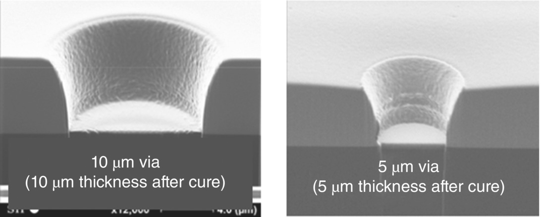
Figure 14.26 Cross sections of PI‐Gen2 vias (5 and 10 μm resolution).

Figure 14.27 PI‐Gen2 cross sections at varying cure temp. (10 μm space, 10 μm cured thickness).

Figure 14.28 PI‐Gen2 cross sections on various substrates (10 μm space, 10 μm cured thickness).
14.15 PI‐Gen2 Material Properties
Mechanical and thermal end‐use properties as well as residual stress are measured to provide performance indicators for dielectric materials in downstream processes used in the manufacture of FO‐WLP devices as well as over the lifetime of the semiconductor device. The mechanical and thermal end‐use properties as well as residual stress for PI‐Gen2 are given in Table 14.17 where it can be seen that, due to the formation of a robust and ductile 3D cross‐linking structure, PI‐Gen2 achieves acceptable end‐use properties, resulting in a wide cure temperature margin over the cure temperature range of 175–250 °C.
Table 14.17 PI‐Gen2 cured film properties.
| Item | Unit | PI‐Gen2 | |||
| Cure temp. | °C | 175 | 200 | 225 | 250 |
| Tensile strength | MPa | 190 | 177 | 175 | 174 |
| Elongation (ave.) | % | 39 | 41 | 40 | 42 |
| Young’s modulus | GPa | 3.4 | 3.3 | 2.9 | 2.8 |
| Tg (TMA) | °C | 225 | 233 | 233 | 242 |
| CTE | ×10−6/°C | 63 | 61 | 60 | 59 |
| Weight loss temp. (5%) | °C | 317 | 336 | 347 | 347 |
| Residual stress | MPa | 25 | |||
PI‐Gen2 showed no significant change in % elongation when measured at ambient temperature and −50 °C (see Table 14.18 and Figure 14.29) on the same mechanical tool, indicating that the % elongation of PI‐Gen2 did not deteriorate at temperatures down to −50 °C. It should be noted that the mechanical tool used was different to that used in generating the data given in Table 14.17 and is the reason why differences in % elongation and modulus were obtained.
Table 14.18 PI‐Gen2 mechanical properties measured at low temperature (−50 °C).
| Sample | Cure temp. (°C/2 h) | Measurement temp. (°C) | Tensile strength (MPa) | Elongation (%) | Modulus (GPa) |
| PI‐Gen2 | 200 | 25 | 141 | 24 | 3.7 |
| −50 | 178 | 20 | 3.7 |

Figure 14.29 PI‐Gen2 mechanical properties. Example of stress–strain curve at 25 °C versus −50 °C.
In addition, while a drop in the modulus and tensile strength was obtained with PI‐Gen2 after 100 hours PCT (121 °C/100% RH, 2 atm.), no change in the % elongation was observed, indicating that PI‐Gen2 has a high moisture resistance that suppresses degradation of mechanical film properties (see Table 14.19).
Table 14.19 PI‐Gen2 mechanical properties after PCT.
| Sample | Cure temp. (°C/2 h) | PCT (h) | Tensile strength (MPa) | Elongation (%) | Modulus (GPa) |
| PI‐Gen2 | 175 | 0 | 190 | 39 | 3.4 |
| 100 | 140 | 37 | 3.1 | ||
| 200 | 0 | 177 | 41 | 3.3 | |
| 100 | 157 | 42 | 3.1 | ||
| 225 | 0 | 158 | 40 | 2.9 | |
| 100 | 146 | 36 | 2.9 |
From the above tests, the main conclusion is that a similar % elongation obtained with PI‐Gen2 at low temperature (−50 °C) as compared to ambient indicates that the cured film is ductile enough to provide crack resistance and so avoid performance issues during component and board reliability testing involving TCT (see section on PI‐Gen2 package reliability performance). In addition, no noticeable change in % elongation after PCT indicates that high moisture resistance is also obtained with PI‐Gen2.
14.16 PI‐Gen2 Dielectric Reliability Data
Reliability testing is undertaken to determine that the dielectric is not degraded in any way during downstream processes that can result in yield losses and also that the performance of the dielectric does not change over the lifetime of the semiconductor device. In this respect, the following tests were conducted on PI‐Gen2:
- Adhesion strength to Cu and PI/PI after PCT.
- Resistance to chemicals used in downstream processing.
- bHAST.
14.16.1 PI‐Gen2 Adhesion After PCT
As discussed previously, delamination at the interface between the dielectric and either the Cu track or another layer of dielectric can induce cracking of both the dielectric material and the Cu track in the RDL layers. In addition, delamination between two dielectric layers can also produce electrochemical migration of the Cu between Cu tracks in the presence of moisture. Therefore, good adhesion of the dielectric to Cu as well as between two dielectric layers is important for package reliability.
The adhesion strength of PI‐Gen2 to Cu and to itself both before and after PCT was measured using the stud test procedure outlined previously. From the test results, it can be seen from Figures 14.30 and 14.31 that PI‐Gen2 cured at various temperatures passed the stud pull test to both Cu and to itself after 300 hours and 200 hours PCT, respectively. In addition, the adhesion results for PI‐Gen2 on 10 μm Cu L/S after 100 hours PCT indicate no delamination when inspected by SEM (see Figure 14.32).

Figure 14.30 PI‐Gen2 adhesion stud pull test results to Cu after PCT.

Figure 14.31 Adhesion stud pull test results to PI‐Gen2/PI‐Gen2 after PCT.

Figure 14.32 PI‐Gen2 cross sections of Cu line after 100 hours PCT at varying cure temperatures.
14.16.2 PI‐Gen2 Chemical Resistance
PI‐Gen2 chemical resistance was tested with the same selection of chemicals as described previously. The results (see Table 14.20 and Figure 14.33) indicated that no changes in either appearance or film thickness were observed with PI‐Gen2 films cured at 175, 200, and 225 °C after immersion in the chemicals tested at a given temperature and time.
Table 14.20 PI‐Gen2 chemical resistance.
| Treatment conditions | PI‐Gen2 | |||||
| Chemicals | Temp (°C) | Time (min) | Check itema, b | 175 °C 2 h |
200 °C 2 h |
225 °C 2 h |
| Rework solvent (NMP) | 25 | 30 | Appearance | No change | No change | No change |
| Film thickness change | OK | OK | OK | |||
| Resist stripper (Dynastrip 7700) | 70 | 30 | Appearance | No change | No change | No change |
| Film thickness change | OK | OK | OK | |||
| Resist cleaner (OK‐73) | 25 | 60 | Appearance | No change | No change | No change |
| Film thickness change | OK | OK | OK | |||
| Flux (WS‐600) | 245 | 1 | Appearance | Slight rough surface | No change | No change |
| Film thickness change | OK | OK | OK | |||
a Appearance No change = no cracking, no delamination, and no hazing.
b Film thickness change % change within ±10% is acceptable.

Figure 14.33 PI‐Gen2 appearance (100 μm square pattern) after immersion in resist stripper.
14.16.3 PI‐Gen2 bHAST
bHAST conducted on PI‐Gen2 showed that, with 5/5 and 2/2 μm Cu L/S, no short circuiting, dendrite formation, corrosion, or delamination was observed for up to 200 hours as indicated by little to no change in the insulation resistance (see Figure 14.34). The test procedure has been described previously, and the test vehicle consisted of 5/5 and 2/2 μm Cu L/S covered by a 7 μm film of PI‐Gen2 cured at 200 °C for two hours.

Figure 14.34 PI‐Gen2 insulation resistance during bHAST (130 °C/85% RH/3.3 V, L/S = 5/5 and 2/2 μm).
14.17 PI‐Gen2 Package Reliability Performance (Component and Board Level)
TCT testing of PI‐Gen2 (cured at 200 °C/2 h) was conducted at both the component and board level. The processing of the FO‐WLP test vehicle is shown in Figure 14.22 together with a cross section of the test vehicle in Figure 14.23. Details of the test vehicle structure are outlined in Table 14.12.
For the component‐level evaluation, the test vehicle was preconditioned at 85 °C/85% RH for 168 hours followed by 10× N2 reflow (260 °C max) and then subjected up to 1000 TCT cycles (−65 °C/15 min ↔ 150 °C/15 min). The test vehicle was visually inspected using an optical microscope for any defects at 200 cycle intervals and where no cracking or delamination was observed after 1000 TCT cycles (see Table 14.21).
Table 14.21 PI‐Gen2 reliability test results after TCT at component and board level.
| Reliability test result (component level) | Reliability test result (board level) | |
| TCT cycles | Appearance after TCT | Cumulative electrical failure rate (%) |
| 0 | No crack or delamination | 0 |
| 200 | No crack or delamination | 0 |
| 400 | No crack or delamination | 0 |
| 600 | No crack or delamination | 0 |
| 800 | No crack or delamination | 0 |
| 1000 | No crack or delamination | 0 |
For the board‐level evaluation, a one‐time reflow treatment (260 °C max) without moisture soaking was used to mount the vehicle onto the board and then subjected up to 1000 TCT cycles (−65 °C/15 min ↔ 150 °C/15 min). As the test vehicle was designed with a daisy chain pattern to measure the electrical resistance across the dielectric between Cu lines, any electrical failure due to solder cracking or cracks to the Cu lines will be detected. In this test, the electrical resistance was measured up to 1000 cycles TCT at intervals of 200 cycles, and no changes in electrical resistance were observed (see Table 14.21).
14.18 Comparison Between PBO‐Gen3 and PI‐Gen2
Both PBO‐Gen3 and PI‐Gen2 meet the challenges previously described at the beginning of the chapter (Table 14.1) for dielectric materials in FO‐WLP applications. The challenges are described as follows, and a more detailed comparison between PBO‐Gen3 and PI‐Gen2 is given in Table 14.22:
- Cure Temperature: PBO‐Gen3 and PI‐Gen2 meet the target cure temperature of <200 °C. In addition, both materials can also be cured over a wide temperature margin ranging from 175 to 250 °C with acceptable end‐use properties.
- Thick Film After Cure: Both materials meet the target maximum cured film thickness of >15 μm, and, while the maximum cured thickness for PI‐Gen2 is currently 15 μm, PBO‐Gen3 can be cured up to 20 μm. This is a noticeable improvement as, historically, PBO‐based positive‐acting, aqueous‐developing systems are difficult to process above cured film thicknesses of 10–15 μm and require noticeably higher exposure energies and longer development times as compared with PBO‐Gen3. In fact, negative‐acting, solvent‐developing materials, due to the lithography technology used (described previously), are typically easier to design for thicker films by optimizing the photo‐package, and, in this respect, development work is in progress to develop a thicker film version of PI‐Gen2 by adjusting % solids and photo‐package levels as well as optimizing pre‐bake conditions.
- Sidewall Shape: After processing, PBO‐Gen3 and PI‐Gen2 both have a smooth profile, no crowning at the top edge of the sidewall, and a sidewall angle of 70–80° to the substrate surface. In this respect, both materials meet the target for sidewall shape with good process control.
- Resolution: Both materials meet the target resolution of <10 μm via opening. PBO‐Gen3 can resolve 2 μm via opening with a 7 μm cured thickness, and PI‐Gen2 can resolve 10 μm via openings with a 10 μm cured thickness as well as 5 μm via openings with a 5 μm cured thickness. As indicated previously, due to the photoinitiator system utilized, positive‐acting systems generally have the advantage of resolving smaller via diameters as compared with negative‐acting systems.
- Deep Gap Formability: PBO‐Gen3 can meet the target of developing a 25 μm pre‐bake thickness after exposure with no residues for applications where it is necessary to open scribe lines after processing multiple RDL. While PI‐Gen2 has not been fully tested to date, being a negative‐acting material, it should be possible to develop a 25 μm pre‐bake thickness with no exposure and, in particular, where high resolution is not a requirement.
- Mechanical Properties: PBO‐Gen3 and PI‐Gen2 have a % elongation >40% when measured at ambient and 20–40% when measured at −50 °C, indicating that both materials are ductile enough to provide crack resistance and so avoid performance issues during component and board reliability testing involving TCT. In addition, no significant change in % elongation was observed after PCT with either PBO‐Gen3 or PI‐Gen2, indicating high moisture resistance with both materials.
- Chemical Resistance: PBO‐Gen3 and PI‐Gen2, when cured between 175 and 225 °C, are resistant to a selection of chemicals used in RDL and bumping processes, which subsequently avoids performance issues such as cracking, delamination, and thickness changes during reliability testing as well as providing a wider process window in downstream processes.
- Adhesion to Cu: PBO‐Gen3 and PI‐Gen2 passed the stud pull test for adhesion after PCT at the Cu/dielectric and the dielectric/dielectric interfaces. In addition, no visual voids or delamination was observed on 10 μm Cu L/S after PCT.
- Insulation (bHAST): No short circuits, dendrite formation, delamination, or Cu migration was observed with either PBO‐Gen3 or PI‐Gen2 after bHAST on test vehicles designed with either 5/5 or 2/2 μm Cu L/S.
Table 14.22 Comparison between PBO‐Gen3 and PI‐Gen2.
| Challenges | Target specification | PBO‐Gen3 | PI‐Gen2 |
| 1. Cure temp. | <200 °C | 175–250 °C | 175–250 °C |
| 2. Thick film after cure | >15 μm cured film thickness | >15 μm | 15 μm |
| 3. Resolution | 10 μm via opening (7 μm cured film) | 2 μm via opening | 10 μm via opening |
| 4. Sidewall shape | 70–80° acute angle to substrate | 75 | 74 |
| 5. Deep gap formability | Develop 25 μm pre‐bake thickness | Max. 25 μm | 25 μm possible |
| 6. Mechanical properties | High elongation at low temp. and after PCT/TCT | >50% at ambient 30–40% at −50 °C and no change after PCT/TCT |
>40% at ambient 20–30% at −50 °C and no change after PCT |
| 7. Chemical resistance | Resistance to chemicals used in FO‐WLP process | Pass | Pass |
| 8. Adhesion to Cu | No delamination at Cu and PI/PBO interface after PCT | Pass after PCT on Cu and PBO/PBO | Pass after PCT on Cu and PI/PI |
| 9. Insulation (bHAST) | No Cu migration during reliability testing | Pass | Pass |
14.19 Summary
To meet the demands of current FO‐WLP applications, it has been necessary to redesign established high temperature cure negative‐acting, solvent‐developing PI and positive‐acting, aqueous‐developing PBO materials for low temperature cure (<200 °C) while, at the same time, addressing challenges in lithography, end‐use performance, and reliability at both the component and board level. As described in this chapter, new generation dielectric materials based on both PI (PI‐Gen2) and PBO (PBO‐Gen3) technologies have been developed that can meet the current requirements of this emerging technology. However, as devices continue to shrink in size while requiring even more I/O connections, there will be an ongoing need to continue development of both PI and PBO materials to meet future performance requirements.
While this chapter has been focused on liquid PI/PBO dielectric materials for FO‐WLP applications, there is also potential for these dielectric materials to be used in embedded die packaging applications where dielectric thin films are typically used. Currently, one of the challenges in using dielectric thin films to process additional prefabrication layers (multilayers) is in laser drilling via holes <20 μm, and while there is a current need for photosensitive dielectric thin films to improve resolution, liquid‐based PI/PBO dielectric materials that have been adjusted for panel processing could meet lithographic and reliability requirements for this application.
References
- 1 Coburn, J.C. and Pottiger, M.T. (1996). Thermal curing in polyimide films and coatings. In: Polyimides Fundamentals and Applications, Chapter 8 (ed. M.K. Ghosh and K.L. Mittal), 207–247. Dekker.
- 2 Rubner, R. (2004). Innovation via photosensitive polyimide and poly(benzoxazole) percursors – a review by inventor. Journal of Photopolymer Science and Technology 17 (5): 685–691.
- 3 Makabe, H., Banba, T., Hirano, T. et al. (1997). A novel positive working photosensitive polymer for semiconductor surface coating. Journal of Photopolymer Science and Technology 10: 307–312.
- 4 Tomikawa, M., Suwa, M., Yoshida, S. et al. (2000). Novel positive‐type photosensitive polyimide coatings “PW‐1000”. Journal of Photopolymer Science and Technology 13: 357–360.
- 5 Nunomura, M., Sasaki, M., Ohe, M. et al. (2000). Hitachi Chemical Technical Report 34: 25–28.
- 6 Hanabata, M., Oi, F., and Furuta, A. (1992). Novolak design concept for high performance positive photoresists. Polymer Engineering & Science 32 (20): 1494–1499.
- 7 Süs, O. (1944). Liebigs Annalen der Chemie 556: 65.
- 8 Monroe, B. and Weed, G. (1993). Photoinitiators for Free‐Radical‐Initiated Photoimaging Systems. Chemical Reviews 93: 435–448.
- 9 Brunnbauer, M., Fürgut, E., Beer, G., et al. (2006). An embedded device technology based on a molded reconfigured wafer. 56th Electronic Components and Technology Conference (2006), pp. 547–551.
- 10 Tseng, C. F., Liu, C. S., Wu, C. H., and Yu, D. (2016). Info (wafer level integrated fan‐out) technology. 66th Electronic Components and Technology Conference (2016), pp. 1–6.
- 11 Töpper, M., Fischer, T., Bader, V. et al. (2011). Ultra low temperature PBO polymer for wafer level packaging application. International Conference on Electronics Packaging (2011), pp. 452–455.
- 12 Windrich, F., Malanin, M., Eichhorn, K.J. et al. (2014). Low‐temperature photo‐sensitive polyimide processing for use in 3D integration technologies. Materials Research Society Symposium 1692: 1–6.
- 13 Shoji, Y., Masuda, Y., Hashimoto, K. et al. (2016). Development of novel low‐temperature curable positive‐tone photosensitive dielectric materials with high elongation. 66th Electronic Components and Technology Conference (2016), pp. 1707–1712.
- 14 Sasaki, T. (2016). Low temperature curable polymide for advanced package. Journal of Photopolymer Science and Technology 29 (3): 379–382.
- 15 Windrich, F., Kappert, E.J., Malanin, M. et al. (2016). In‐situ imidization analysis in microscale thin films of an ester type photosensitive polyimide for microelectronic packaging applications. European Polymer Journal 84: 279–291.
- 16 Enomoto, T., Abe, S., Matsukawa, D. et al. (2017). Recent progress in low temperature curable photosensitive dielectrics. International Conference on Electronics Packaging (2017), pp. 498–501.
- 17 Tomikawa, M., Matsumura, K., Shoji, Y. et al. (2017). Development of photosensitive polyimide B‐stage sheet having high Cu migration resistance. Journal of Photopolymer Science and Technology 30 (2): 181–185.
- 18 Mitsukura, K., Abe, S., Toba, M. et al. (2016). Highly reliable Cu wiring layer of 1/1 m line/space using newly designed insulation barrier film. 49th International Symposium on Microelectronics (IMAPS2016), pp. 165–170.
- 19 Toba, M., Mitsukura, K., Ejiri, Y. et al. (2017). Ultra‐fine Cu wiring surrounded by electroless‐plated Ni: effective structure for high insulation reliable wiring applicable to panel level fabrication. 50th International Symposium on Microelectronics (IMAPS2017), pp. 742–746
- 20 Anzai, N., Fujita, M., and Fujii, A. (2014). Drop test and TCT reliability of buffer coating material for WLCSP. 64th Electronic Components and Technology Conference (2014), pp. 829–835.
- 21 Fujita, M., Fujii, A., Shimoda, S., and Kariya, Y. (2015). TCT reliability of organic passivation layer for WLCSP. 48th International Symposium on Microelectronics (IMAPS2015), pp. 505–509.
- 22 Chen, Y.C., Wan, K., Chang, C.A., and Lee, R. (2017). Low temperature curable polyimide film properties and WLP reliability performance with various curing conditions. 67th Electronic Components and Technology Conference 2017, pp. 2040–2046.