
18
Tools for Fan‐Out Wafer‐Level Package Processing
Nelson Fan, Eric Kuah, Eric Ng, and Otto Cheung
ASM Pacific Technology
18.1 Turnkey Solution for Fan‐Out Wafer‐Level Packaging
In this chapter, we discuss three critical processes for fan‐out wafer‐level packaging (FO‐WLP) technology. They are die placement, large format encapsulation, and handling of finished packages after singulation. Unlike traditional packaging platforms, the majority of FO‐WLP is being manufactured in 12 in. wafer formats rather than small strip formats. Moreover, the FO‐WLP technology platform is flexible as it can address different device design requirements with densely routed redistribution layers (RDL) and by deploying many different die placement approaches, such as chip‐first and chip‐last coupling with either a local or global alignment method. Depending on which approach is being used, the die placement can be done at room temperature or at an elevated temperature with die facing up or facing down. During molding, the reconstructed wafer can also be molded with either die face‐up or face‐down orientation, depending on the package structure. Specifically, the latter is deployed for process designs comprising molded underfill (MUF) processes. Often, packaging subcontract manufacturers offer multiple fan‐out approaches to their customers; therefore, the required die placement tool and encapsulation tool both have to be able to handle large format material and be flexible and robust enough to cater to different process requirements. After the package singulation process, the individual units will be handled by post‐singulation handling systems designed for testing, laser marking, final all‐sided inspection, and tape and reel packing. In order to ensure good quality output for downstream surface‐mount technology (SMT) assembly, the test handling system needs to have a reliable optics system for inspection and a chip component handling system to avoid inducing further defects to the tested objects. The details will be discussed in the subsequent sections. Figure 18.1 shows the tools developed for the manufacturing of FO‐WLP.

Figure 18.1 Turnkey solution for FO‐WLP.
18.2 Die Placement Process and Tools for FO‐WLP
Today, advanced packaging technology innovation is increasingly important for driving the enhancement of package performance, lowering cost, and achieving a small form factor. Enabled by thin film‐based interconnects, various FO‐WLP packaging technologies such as embedded wafer‐level ball grid array (eWLB) [1], integrated fan‐out (InFO) [2], and fan‐out chip on substrate (FOCOS) [3] have emerged and evolved to potentially replace many current packaging technologies from low and high density 2D packages like flip‐chip chip‐scale packages (FCCSP) to high‐end 2.5D packages like chip on wafer on substrate (CoWoS) and even 3D packages like molded core embedded packages (MCeP) and high bandwidth package on package (HBPOP) for different applications. eWLB, as an example of a low density 2D package, has been a good replacement for conventional FCCSP with a cost‐effective process and a thin package profile due to its substrate‐less nature [1]. Normally, in FCCSP manufacturing, flip‐chip bonding of the chip with solder bumps occurs onto a laminated substrate in a small strip format followed by a reflow process and MUF. In eWLB manufacturing, which is a chip‐first approach, meaning the chip is bonded prior to an RDL process, the chip is first bonded onto a double‐sided adhesive laminated onto a 300 mm diameter carrier followed by wafer‐level compression molding. After molding, the RDL circuitry is deposited onto the active chip area and the mold compound surface at the periphery of the die by means of thin film technology. Unlike FCCSP, without the use of substrate, the overall package thickness of eWLB is reduced. It is also a more cost‐effective process by making use of batch processing in large format manufacturing [1].
For higher density package designs, the InFO package, which is also a 3D package, sets another reference for using FO‐WLP technology as an alternative to package‐on‐package (PoP) structures for mobile application processor devices [2, 4]. FOCOS is yet another example of even higher density FO‐WLP with heterogeneous integration capability to substitute 2.5D packages with TSV Si interposers for high‐end applications such as networking servers and high performance computing [3]. It is achieved by high density RDL technology with tight line width and spacing (L/S) scaling at 2 μm and below.
Another way to achieve 2.5D substitution can be done by the chip‐last FO‐WLP approach, in which the chip is flip chip bonded followed by reflow onto a prefabricated high density RDL on top of the temporary carrier. Each of these fan‐out packaging technologies has unique features and merits in terms of form factor, electrical and thermal performance, package reliability, and cost‐effectiveness. Figure 18.2 summarizes the various fan‐out packaging technologies that are alternative solutions to the current packaging technologies described above.

Figure 18.2 Use of various thin film fan‐out packaging technologies.
Different FO‐WLP approaches are achievable by different process steps and sequences. Figure 18.3 illustrates the major processing steps of various fan‐out packaging technologies. It shows the different ways for chip placement. In the first approach, the chip is bonded on a 200 or 300 mm diameter mother wafer by means of die‐attach film (DAF) bonding. Chip orientation, which is defined as the orientation of the active side of the chip when it is bonded, is face‐up. The second approach shows an example of achieving heterogeneous integration by FO‐WLP in a multi‐chip module package configuration. Unlike the first approach, a chip is bonded on the wafer carrier with a prefabricated RDL with the chip orientation facing down. Here, the interconnect can be achieved by either mass reflow soldering or the more advanced thermal compression bonding (TCB) process.

Figure 18.3 Illustrations of the major processing steps of various FO‐WLP technologies.
The die placement process for each type of these fan‐out packaging technologies can be characterized in different ways: (i) die placement orientation, (ii) die alignment mode, (iii) die placement process condition, and (iv) die placement accuracy.
Die placement orientation can be classified into two modes. They are the face‐up and face‐down modes. The former has the die active side face‐up during die placement, and the latter has the die active side face‐down. Die alignment modes include local alignment and global alignment. Local alignment mode uses a local alignment mark near the bond position locally as a reference. Global alignment mode, on the other hand, uses a common alignment mark on the carrier or substrate carrier as a reference.
Die placement process conditions can be classified in two common ways: (i) at room temperature and (ii) at elevated temperature and force. For the room temperature process, it can be face‐down bonded onto a temporary adhesive or flip chip bonded on a prefabricated RDL with solder bumps. Temperature and force processes may be referred to as DAF bonding. The chip is bonded at an elevated temperature with force onto the carrier. Depending on the DAF material, the bond temperature ranges from 80 to 150 °C, while the bond force is usually below 200 N, which also depends on the die size. Depending on where the DAF is applied, heating can be applied to the bond head and/or the bond stage.
The die placement accuracy requirement depends on the RDL routing density. A higher RDL routing density requires tighter placement accuracy. There are placement accuracy requirements at or below 10, 5, and 3 μm, respectively.
Figure 18.4 summarizes all the necessary features that are required to handle the die placement tool in terms of various fan‐out packaging technology requirements.

Figure 18.4 FO‐WLP die placement tool suitable for various FO‐WLP technologies.
18.3 Encapsulation Tool for Large Format Encapsulation
Large format encapsulation refers to compression molding onto a substrate that can be either 200 or 300 mm in diameter or rectangular shaped. The compression molding equipment that is currently available in the market is able to handle both of these substrate formats. There are two main advantages of using compression molding for FO‐WLP as opposed to other forms of encapsulation such as transfer molding. Firstly, compression molding allows for more flexible package thicknesses as the thickness is determined by the amount of encapsulant, while transfer molding uses a fixed tool set; thus a change of package thickness requires a new molding tool [5]. Secondly, compression molding is film assisted, and the encapsulant is directly dispensed onto the substrate. Thus there is no requirement for mold cleaning, which can be translated into more uptime for manufacturing of the package. For transfer molding, the end user will still have to maintain cleanliness for the transfer mechanism because the encapsulant introduced into the mold cavity in pellet form will be transferred from the plunger and pot system that come into direct contact with the encapsulant [7]. Circular is the most common substrate format, and it can either be used in its original form or be mounted onto some other form of carrier. This is because most post‐encapsulation processes are generally designed to handle circular formats. Metal and glass are most commonly used for the carrier [6]. However, such carriers are generally custom manufactured to have the coefficient of thermal expansion (CTE) that is as close as possible to the encapsulant (epoxy based) and the silicon die [6].
Compression molding can be performed with the active side of the silicon die face‐up or face‐down depending on the package configuration. The substrate is either substrate face‐up or substrate face‐down with reference to the bottom chase (see Figure 18.5). Substrate face‐down placement is used when there is a challenge to resolve mold voids. Placing the substrate in a face‐down direction allows it to have more time for the evacuation of air from the molding tool, and the encapsulant can be preheated without contact with the silicon die attached to the carrier before compression molding [6, 7].

Figure 18.5 Direction of molding.
Generally, the compression molded package is molded with a keep‐out‐zone (KoZ) outline, which means that the package outline is smaller than the dimension of the carrier (see Figure 18.6). Table 18.1 is a comparison of three different manufacturers of compression molding equipment that can be used for encapsulating FO‐WLP. Generally, all three manufacturers have the required tonnage and necessary features for molding FO‐WLP packages. However, one key requirement for molding multi‐die FO‐WLP when using liquid encapsulant, the most commonly used form of encapsulant [5], is the ability to dispense patterns beyond glob tops (see Figure 18.7). In Table 18.1, manufacturer C does not have the capability to dispense more than one dispensing pattern for liquid encapsulants.

Figure 18.6 Definition of keep out zone (KoZ).
Table 18.1 Comparison of compression system from three manufacturers.
| Firm | Expandable/press | Mode of molding | Tonnage (T) | Handler | Mold clean | 5S/6S in a single system | Liquid dispensing capability | Overmold capabilities | Thinnest mold cap (μm) | Largest substrate (mm2) |
| A | Yes/2 | Die‐up, die‐down | 60 | Customize robot for face‐up/face‐down molding | Yes | Yes | Multiple patterns | Yes, without FAM | 35 | SQ 340 mm |
| B | Yes/2 | Die‐down | 80 | Normal robot and loader | No | No | Glob via spinning | No | 300 | SQ 320 mm |
| C | Yes/2 | Die‐up | 36 | Normal robot and loader | No | No | Glob | Yes with FAM | 200 | SQ 300 mm |

Figure 18.7 Various dispensing patterns to resolve moldability challenges.
Braun [5] and Kuah [7] have shown that in order to overcome moldability challenges such as flow mark and incomplete fill, glob top dispensing patterns at the center should not be used. Dispensing patterns such as maze, star, and serpentine should be used instead, as they allow the encapsulant to cover a wide area on the substrate and result in short mold flow paths [7] (see Figure 18.8). This ability to dispense multiple types of dispensing patterns will help to solve moldability challenges such as flow mark and incomplete fill [5, 7]. However, it can be overcome by designing a dispensing table that can travel in x–y directions with the dispenser mounted in a fixed position (see Figure 18.8). Although manufacturer A has the capability to mold very thin mold caps, this is not required for FO‐WLP; however, five‐ and six‐sided wafer‐level packaging (WLP) does require thin mold caps [6].

Figure 18.8 Dispensing with x–y table movement.
A typical compression encapsulation tool is made up of input/output modules, mold press, mold chase, aligner, dispenser, and automatic handlers. It is noted here that there will be some variations among the different vendors shown in Table 18.1, but the basic compression encapsulation system is still very similar in configuration.
Figure 18.9 shows the input/output modules that can be configured to accept wafers of up to a maximum of 300 mm circular format (shown at the left side of Figure 18.9). For other formats, such as metal carriers larger than 300 mm, a cassette will be used instead (shown at the right side of Figure 18.9).

Figure 18.9 Input and output load ports for different substrate formats.
Figure 18.10 shows the molding press installed with the mold chase. It is not notably special, except that the design could be configured to accept both types of mold tooling for either substrate face‐up or substrate face‐down molding.

Figure 18.10 Molding press system with convertible mold chase.
Above is a dispenser that can be configured for both liquid (Figure 18.11a) and granular (Figure 18.11b) encapsulants.
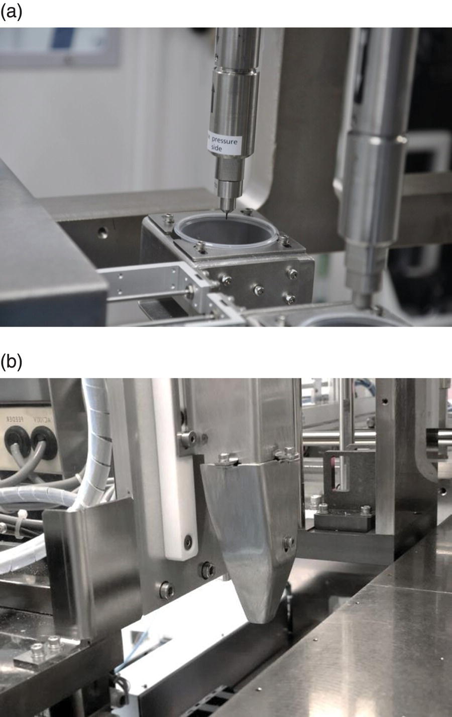
Figure 18.11 (a) Dispenser for liquid. (b) Dispenser for granules.
Lastly, Figure 18.12 shows a SCARA robot handler transporting the substrate from the input module to the aligner and then to the dispenser, followed by the mold press. Once molding is completed, it will transport the molded substrate back and place it into the output module.

Figure 18.12 SCARA robot handler.
18.4 The Test Handling and Packing Solution for Wafer‐Level Packaging and FO‐WLP
Final packing is an important process that requires good quality output before conducting SMT placement onto a printed circuit board. Detecting micro‐defects is extremely important to ensure the final quality. A system comprising a series of processes including final testing, laser marking, and final all‐sided inspection is needed to achieve the goal of good quality output for FO‐WLP and fan‐in WLP today. A few types of equipment can be applied to work on this procedure, though the turret platform is definitely the only way to provide an all‐in‐one solution in one system (see Figure 18.13).

Figure 18.13 All‐in‐one total solution using turret platform with final testing, laser marking, all‐sided inspection, and packing.
The turret platform provides a total solution for both fan‐in and FO‐WLP final packing applications with the most advanced technologies to address today’s high quality requirements. Contactless précising is a noncontact solution to ensure die placement accuracy without the risk of creating die defects during handling. A‐Eye inspection is the latest technology used for WLP micro‐crack detection. Additionally, the Smart iFlip solution for handling ultrasmall WLP especially during system conversion is all essential to overcome today’s challenges.
Contactless précising refers to the handling of packages without any physical contact. The system uses vision to locate the package position, and the pick head is built with an individual rotary motor for angular rotation. Submodules like test modules or offload modules will move in x–y directions to align with the package (see Figure 18.14).

Figure 18.14 Contactless précising for aligning package with modules in the x–y direction.
A‐Eye technology provides smart optical and algorithm solutions for WLP defect detection. Systems equipped with microscopic grades of lenses with autofocusing functions provide the best image quality. Algorithms with smart filtering functions are able to locate cracks without overkilling from background noise such as saw marks and step cuts (see Figure 18.15) while maintaining yield in mass production. With this A‐Eye technology, the system is able to detect micro‐cracks of less than 3 μm in size, whereas the other market solutions are only capable of 5–10 μm.

Figure 18.15 A‐Eye inspection detecting micro‐crack width with autofocusing function and smart noise filtering algorithm.
Smart iFlip solution, as a fast conversion tool, automatically locates all the combinations of turret heads and flipping heads by vision inspection. The flipper module will then index accordingly based on the vision inspection results (see Figure 18.16), which greatly reduces the conversion time for ultrasmall WLP without any need for manual adjustment.

Figure 18.16 iFlip function reduces the setup time for ultrasmall‐size WLP.
References
- 1 Brunnbauer, M., Fürgut, E., Beer, G. et al. (2006). An embedded device technology based on a molded reconfigured wafer. IEEE/ECTC Proceedings, 2006, pp. 547–551.
- 2 Tseng, C.‐F., Liu, C.‐S., Wu, C.‐H., and Yu, D. (2016). InFO (wafer level integrated fan‐out) technology. IEEE/ECTC Proceedings, 2016, pp. 1–6.
- 3 Lin, Y.‐T., Lai, W.‐H., Kao, C.‐L. et al. (2016). Wafer warpage experiments and simulation for fan‐out chip on substrate. IEEE/ECTC Proceedings, 2016, pp. 13–18.
- 4 Hsieh, C.‐C., Wu, C.‐H., and Yu, D. (2016). Analysis and comparison of thermal performance of advanced packaging technologies for state‐of‐the‐art mobile applications. IEEE/ECTC Proceedings, 2016, pp. 1430–1438.
- 5 Braun, T., Voges, S., Kahle, R. et al. (2015). Large area compression molding for fan‐out panel level packing. IEEE/ECTC Proceedings, 2015, pp. 1077–1083.
- 6 Che, F., Ho, D., Ding, M., and Zhang, X. (2015). Modeling and design solutions to overcome warpage challenge for fan‐out wafer level packaging (FO‐WLP) technology. IEEE/EPTC Proceedings, 2015, pp. 2–4.
- 7 Kuah, E., Hao J.Y., and Chan, W.L. (2016). Wafer level encapsulation – an alternative format for discrete packaging: its challenges and solutions. Proceeding of International Wafer‐Level Packaging Conference, 2016, pp. 1–8.