
11
Embedded Die in Substrate (Panel‐Level) Packaging Technology
Tomoko Takahashi and Akio Katsumata
J‐Devices
11.1 Technology Description
With square or rectangular panels instead of circular wafers, panel‐level packaging has more die per panel than an equivalent size round wafer with its edge and missing die losses, potentially providing significant cost savings. Similar to other advanced packaging techniques, a fan‐out (FO) technique is required to achieve higher integration levels and a greater number of external connections. The fan‐out panel‐level package (FO‐PLP) described in this chapter is unique, because a metal material was selected as the base plate of an FO package. The base plate was not a temporary structure to place die on, but was a part of the package as shown in Figure 11.1.
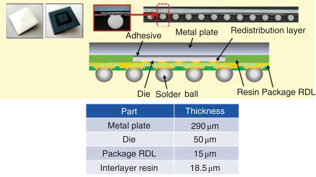
Figure 11.1 Fan‐out package using a metal base plate.
The main technology issue of panel‐level assembly is how to laminate resin, similar to the substrate manufacturing process using laminate dielectric layers, on metal without delamination, warpage, or deformation during processing. To address this issue, J‐Devices adds a stress release layer between the metal and the resin. This layer releases the stress caused by the coefficient of thermal expansion (CTE) mismatch among layers during the assembly process. With this approach, the warpage of the panel is well controlled and can be handled in each process step.
The FO‐PLP reported in this chapter has good reliability and very low warpage. The design is extremely flexible and has several possible applications, including automotive, mobile, and antenna electronics. The initial design provides a package suitable for in‐vehicle use. For mobile applications, thinner packaging is needed. For antenna use, the metal plate disturbs antenna wave irradiation. To address this issue, removing the metal plate became necessary. All three of these design targets were achieved with embedded die in substrate (EDS) package technology. Its detail and variations will be introduced in the following sections. Based on the design differences for different applications, there are two different EDS technology sections at the end of this chapter that explain the enhancements for smartphone modules and power devices.
11.2 Basic Package Construction
A cross‐sectional view of the standard EDS package is shown in Figure 11.2. The thickness of the die can be from 35 to 100 μm, and the resin thickness can be selected from several options. The thickness of resin on the topside impacts the package warpage, so the proper thickness must be determined for each design. The thickness of each layer in Figure 11.2 is the result of extensive development efforts.

Figure 11.2 EDS package design characteristics.
As shown in Figure 11.2, the surface of the package is covered with top resin to protect the package. It is not a base plate of the panel, so it is not the essential part of the package. If pads are needed on the topside of the package, the topside resin can be removed. The cross‐sectional structure with pads on both sides is shown in Figure 11.3. The pads on both sides of the package enable a package‐on‐package (PoP) design.

Figure 11.3 EDS with pads on both sides of the cross‐sectional structure.
11.3 Manufacturing Process Flow and BOM
A basic process flow for FO‐PLP is shown in Figure 11.4. Wafers that have Cu lands on the die pads are prepared before assembly. Die pads should be covered by Cu metal, because a laser via is directly formed over the die pad. Cu is the protective layer for laser irradiation. After Cu lands are formed over die pads, wafers are diced into individual die.

Figure 11.4 Basic FO‐PLP processing steps.
Next, die are mounted on to the panel with a panel‐level die attach machine. They are embedded by resin lamination, and via holes are laser‐etched into the embedding resin to connect the top of the embedding resin to the Cu lands on the die. The Cu trace layer is formed onto the resin layer by the semi‐additive process (SAP) method, and the next resin layer is formed on the Cu trace layer. By repeating resin formation, trace plating by SAP, and laser‐etched via holes, multiple Cu trace layers are formed. The pads are formed on the outermost trace layer. After the outermost trace layer is completed, the solder resist (SR) layer is formed. Following this step, solder balls are attached and packages are diced.
For EDS, the process is shown in Figure 11.5. The base plate for EDS consists of a metal layer and resin layers. EDS needs trace layers under the die to have pads on both sides of package, so the layers are assembled onto the base plate before die mount. A resin layer is formed on the base plate. Via holes are laser‐etched into the resin. The Cu trace layer is formed onto the resin layer by the SAP method, and the next resin layer is formed on the Cu trace layer.

Figure 11.5 EDS processing steps.
After the required layers are formed, die are mounted on the panel by a panel‐level die attach machine. They are embedded by resin lamination, and via holes are laser‐etched into the embedding resin to connect the top of embedding resin to the Cu lands on die. Also, deep via holes connect the top of the embedding resin to the Cu lands of traces on the bottom layers. Trace layers of the topside are formed by repeating resin formation, trace plating by SAP, and laser‐etched via holes. A seed layer is formed by electroless plating of SAP process. The pads are formed on the outermost trace layer. After the outermost trace layer is completed, the SR layer is formed. The next step is the base plate removal. Removing the base plate, the bottomside of panel appears on the surface. To protect the package resin layer on the bottomside, an SR layer is formed. Balls are mounted in the panel level, and the panel is diced into units to complete the EDS package.
There are three key challenges in EDS process technology. The first is die mount technology. Achieving good position accuracy of die placement is very important for each company that develops FO packaging technology. For EDS technology, the required position accuracy is about 10 μm. This accuracy affects the Cu land size on the die. A small Cu land size means a small die pad pitch, and conversely, a small die pad pitch means a small die size. Consequently, accurate die mount technology is very important for shrinking the package.
The second key area is the semi‐additive processing technology. SAP is a very general technology for trace formation in organic buildup substrates. The line and space (L/S) of the trace are not as small as the wafer‐level photolithography technology, but substrate plating technology can achieve panel size plating. As shown in Figure 11.6, three times the number of packages on one wafer‐level assembly can be achieved on one panel. This approach is very effective for high volume products.

Figure 11.6 Area effect of wafer‐level packages on one panel‐level structure.
The third key area for EDS is the method to remove the base plate. The base plate can be removed clearly and easily after almost all trace layers are assembled on the panel. At this point, the warpage of the panel is not a major problem for the remaining processes.
11.4 Design Features
The design rules of package trace layers are shown in Figure 11.7. The L/S design rule is 20 and 20 μm. This is a very standard value of a buildup‐type substrate. The via land is 65 μm in diameter, so the via pitch for different signals is 85 μm. To minimize via area or for better electrical performance in via area, via stacking is the key solution. Stacked via structures have been qualified and a four‐stacked via is acceptable to use. The design rule of the deep via that connects between the layer over the die and the layer under the die is determined by the die thickness and layer structure. Figure 11.8 shows a very standard example. In the case of 50 μm die thickness, via of 97 μm depth and 120 μm diameter have been qualified. The L/S are 20 μm/20 μm and via hole size is 23 μm in diameter. The via land is 65 μm for a 23 μm via hole. Considering the accuracy of die mount and reliable connection at the via bottom, the size of the via land and hole is the minimum for the process.

Figure 11.7 Design rules for a typical EDS package.
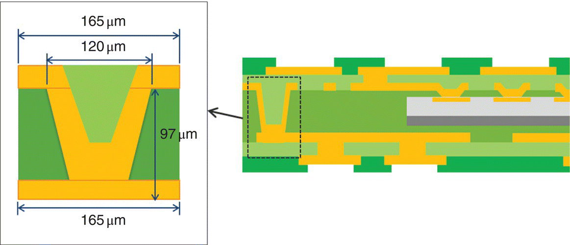
Figure 11.8 Example of a standard deep via between topside and bottomside of an EDS package.
To determine the best package size for a panel‐level assembly package, the assembly yield must be considered. In the case of a very standard design rule such as the one shown in Figure 11.8, L/S = 20 μm/20 μm and a 23 μm via hole, most of the failures are caused by foreign material in the manufacturing process, not open or shorted traces. If the package size is increased, the possibility of foreign material over one package becomes bigger.
11.5 System Integration Capability
EDS technology can have many variations of layer structures, package size, die counts, and more. Stacking die in a package, shown in Figure 11.9, has already been achieved. The EDS package can have terminals on both sides. Also, components can be mounted over the EDS package. When this is done, the EDS package becomes a module structure. The technology details of such a module are explained further in Section 11.7. Also, it is easy to form side‐by‐side structures, because die can be placed in 150 μm pitch and can be connected to each other by via holes and traces.

Figure 11.9 Stacked die EDS structure.
Design flexibility and the number of design possibilities are strong points of EDS technology. Design flexibility means not only layer counts but also the number of die and various die positions. Samples of various structures are shown in Figure 11.10. The top left hand is a single die, the top right hand shows two die, the lower left hand shows the interconnection of several die, and the lower right shows two die that require close proximity for improved signal communications. The capability of including and connecting several die in a package is one of the key advantages for EDS, allowing the technology to achieve a system‐in‐package (SiP) design. To minimize the system, connecting active die in one package is significant.

Figure 11.10 Possible EDS alternatives.
11.6 Package Performance
11.6.1 Thermal Performance Comparison Between EDS and FBGA
Figure 11.11 shows the results of a thermal performance comparison between an EDS and a fine‐pitch ball grid array (FBGA) package. The metal plate under the EDS die provides a good heat spreader, so the thermal resistance is lower than that of an FBGA. The thermal resistance was reduced by 30% for θja and 40% for θjc. Of course, the main heat dissipation occurs at the second‐level assembly board. To reduce thermal resistance in the system, the assembly board should be designed carefully for optimum heat removal. Comparisons with FC‐CSP, FO‐WLP, and other embedded technologies are expected to show improvements as well, although not necessarily as great.

Figure 11.11 Thermal performance comparison between an EDS and an FBGA package.
11.6.2 Electrical Performance Comparison Among EDS, FC‐BGA, and FBGA
EDS technology does not use a substrate in the package, like a flip‐chip ball grid array (FC‐BGA) or wire‐bond BGA (WB‐BGA). In packages using a substrate, a connecting structure between die and substrate such as a solder bump, Cu pillar, wire, or other electrical connection is required. Reflection of electrical waves happens at impedance uncontrolled points. It is difficult to match impedance completely at the connection point. The connection structure becomes a reflection point or gap for the electrical wave [1]. Consequently, the structure should be as small as possible for good signal integrity at high frequencies. In the EDS package, the via connecting the die and the signal trace is small, just 23 μm in diameter and 18 μm thick. In contrast, a WB‐BGA package’s connection between die and signal trace is wire, 18 μm in diameter and from 1 to 3 mm in length, and an FC‐BGA’s connection is solder bumps, 70 μm in diameter and around 50 μm in height. The EDS packages’ connection points are smaller, when both its connectivity diameter and length are taken into account, compared with other packages’ connection points.
In general, the package’s substrate provides another gap point for an electrical wave. Generally, buildup substrates have core layers. The core layer is thicker than the buildup layers and includes glass cloth in the resin. Since the plating through‐hole is drilled in the core layer, it is larger than a laser via hole in the buildup layers. The long length and thick plating of the drilled through‐hole in the core layer becomes a large gap in the electrical wave route. In comparison EDS has no core layer and benefits from the smaller laser via hole.
The insertion losses of several packages are shown in Figure 11.12. The difference between FBGA and EDS losses is very clear at any frequency. The FC‐BGA and EDS package losses are almost the same until 10 GHz, but over 10 GHz, the difference is clear. The insertion losses of the EDS package are less than others. Improvements are also expected when comparing EDS with FC‐CSP, FO‐WLP, and other embedded technologies although they may not be this significant. Considering this analysis, the EDS package is suitable package for millimeter wave applications. EDS packages have already been developed for 80 and 40 GHz designs.

Figure 11.12 Insertion loss simulation for various packages.
For radio frequency (RF) applications, a high frequency package design is needed. The package also needs to integrate a variety of components. As shown in Figure 11.12, the EDS package can achieve excellent performance at over 20 GHz, and a module structure is possible for EDS technology that will be shown in Section 11.7. The combination of these two attributes makes the EDS package a suitable choice for RF applications. For now, RF applications are mainly in smartphones, but they will also be appropriate for many other Internet of things (IoT) applications as the market needs grow.
11.6.3 Robustness and Reliability Data
The basic process of the FO‐PLP package with metal base plate has good reliability. The data shown in Figure 11.13 is for a 12 mm × 12 mm package with 360 balls at 0.5 mm ball pitch. The test is done by electrical connection (short/open) and confocal scanning acoustic microscopy (CSAM) measurements. The conditions are based on the Automotive Electronics Council (AEC) Q‐100/Grade 0. The FO‐PLP with metal plate has good reliability and passed the required reliability level for automotive applications. The FO‐PLP’s warpage data is shown in Figure 11.14. The warpage does not change at any temperature indicating the stress in the package is very small.

Figure 11.13 Package cross section (a) and reliability test results (b) of FO‐PLP design.

Figure 11.14 Warpage measurements for FO‐PLP design.
The reliability data for the EDS package of Figure 11.10 is shown in Figure 11.15. In this case, the package size is 3.6 mm × 3.6 mm with 81 balls at 0.35 mm ball pitch. The testing was performed based on JEDEC standards and was checked by electrical connection and CSAM measurements. All test samples passed. More information about EDS module reliability is provided in the next section.

Figure 11.15 EDS reliability test matrix.
11.7 Diversity of EDS Technology: Module
11.7.1 Technology Description
For smart phone applications, design requirements include small and thin packages. To make the system smaller, the package needs to include die, components, and more, in other words, an SiP design. As shown in Figure 11.3, EDS technology can assemble a package that has outer leads on both sides. Furthermore, as introduced in a previous section, EDS technology can include more than two die in one package. With these basic technologies, a module structure using EDS technology has been developed. The details are discussed in this section.
11.7.2 Basic Package Construction
The basic structure of a module using EDS technology is shown in Figure 11.16. Components mounted on the topside of an EDS package with both side leads are protected in the overmold structure. In addition, various component heights can occur. Normally, if components are mounted in a resin layer, it is difficult to control the resin flatness over the layer where components with different heights are embedded. To avoid such issues, components were placed on the topside of EDS package. Using this design approach, various types of components can be mounted. Molding components is recommended since the mold resin protects components and their connections in the package, but molding is optional. For the molding process, compression molding with molded underfill (MUF) is recommended.

Figure 11.16 A module using EDS technology.
11.7.3 Manufacturing Process Flow
The process flow for the EDS package was discussed in an earlier section. After SR formation of the EDS package, the panel is cut into strip shapes for components mounting. The strip size is 74 mm × 240 mm. After components are mounted and reflowed, the strip is molded by compression mold with MUF, then the balls are mounted and reflowed in strip style, and the strip is diced into packages. Selecting the optimum mold resin material is one of the key aspects of this structure. Since the warpage of the panel or strip or package differs greatly between designs, the proper mold resin must be chosen for each design.
11.7.4 Design Features
For modules, the basic design rule is the same as shown in Figure 11.7. Figure 11.17 shows the design rules required for die, via, and component placement. The distance B between die was decided from mount accuracy and resin flow. Dimensions A and C were decided based on package dicing accuracy. An example of the cross‐sectional analysis for each layer’s thickness is shown in Figure 11.18. The mold thickness on components is normally controlled at twice the filler size in the mold resin.

Figure 11.17 Design rules for an EDS module.

Figure 11.18 Cross‐sectional analysis of an EDS module.
11.7.5 Robustness and Reliability Data
In addition to the basic EDS testing shown in a previous section, reliability tests were conducted on basic EDS module samples with the structure shown in Figure 11.16. Figure 11.19 shows the test criteria and results. The package size was 5 mm × 5 mm with 40 land grid array (LGA) at 0.4 mm pitch. The testing was performed based on JEDEC standard and also was checked by electrical connection (continuity) and CSAM measurements. Test units passed the established criteria with no failures. This reliability testing qualifies the basic EDS module structure. However, since the module design is customized for each system, reliability should be verified for each system.

Figure 11.19 Module reliability test matrix and results.
11.7.6 System Integration Capability
Another EDS module example is shown in Figure 11.20. This system includes two die, wafer‐level chip‐scale packaging (WLCSP), and various passive components. The die are stacked in the package and not mounted side by side. WLCSP and components are mounted on the package.

Figure 11.20 Example of an EDS module with WLCSP.
In this SiP design, the system’s size was reduced by 35% in area from the original system that contained several packages. EDS technology provides considerable design flexibility, so a variety of SiP designs can be easily achieved.
11.8 Diversity of EDS Technology: Power Devices
11.8.1 Technology Description
Power electronics is very important in many industrial fields [2]. Power semiconductors, including MOSFETs, insulated‐gate bipolar transistors (IGBTs), and other devices, have been used for many years as essential parts of power electronics for controlling or switching the current from the power source. Recently, in automotive applications, the demand for electric and hybrid vehicles has increased because of their fuel efficiency and concerns about environmental pollution problems. The power devices in the power electronic circuits in those automobiles require high density assembly to obtain intelligent, high powered, and reliable control [3]. Additional requirements for each power device dictate that its packaging has small size, high thermal performance and is fabricated with low cost manufacturing [4]. However, conventional power device packages have miniaturization and cost limits due to the use of a wire‐bonding process where each bond is fabricated one at a time. Moreover, the thermal performance is also restricted because the thermal flow inside the package only has a single path through the narrow metal wires to dissipate outward. Consequently, a new package with both small size and high thermal performance is desirable.
With the above background, a new and expandable advanced package using EDS technology for power devices that matches the desired requirements is discussed in this section. The package uses a type of multilayer laminated construction and can be fabricated using a printed circuit board (PCB) process. Power device chips are embedded in the laminated resin layer. The package size is very small and very thin with precise trace patterning. The traces are formed by process integration of insulator lamination, via formation, metallization, and subtract etching. At insulator lamination, the thickness of insulator on the embedded die should be well controlled because it strongly affects the quality of via size and metal filling in the following process. And at the metallization process, precise control of the thickness of the metal is very important for fine pattering at the following subtract etching. In addition, the package has good thermal performance with low thermal resistivity and high power dissipation as discussed on later in this section. Moreover, the package design has very low drain to source on‐resistance with low resistivity connections using many via holes as shown in Figure 11.22. The package uses a redistribution layer (RDL) of a trace and multilayer structure, so the pattern layout is easy to customize. With this design methodology, there can be many types of devices including discrete or power module systems with integrated control driver chips.
11.8.2 Basic Package Construction
Figure 11.21 shows the outline of a basic EDS package for discrete power devices. The discrete MOSFET power device has only three pads: source, drain, and gate. Most chips for power devices are a vertical‐type design that has a source pad and gate pad on one side (usually the top) and a drain pad on the other (usually the bottom).

Figure 11.21 Outline of a basic EDS package for power devices: (a) bottom and (b) top.
The cross‐sectional view in Figure 11.22 is a facedown design. The chip is embedded in an insulator resin, and the gate or source pads are connected on the bottomside of the package through shallow vias. The drain pad is connected on top through a bottom via and connected to the bottom package side through the package’s deep via. Three types of contact vias are designed for each of the pads: on the top of and near the die through the insulator resin and under the die through the die attach film (DAF).

Figure 11.22 Cross‐sectional view of a facedown EDS power package.
11.8.3 Manufacturing Process Flow
The process flow of the EDS power package is shown in Figure 11.23. Starting with the formation of layer 1 (L1, die attach mark) to layer 2 (L2, top trace layer), the process is same as a typical EDS process. The only difference is the formation of layer 3 (L3): bottom vias and bottom trace layer. In the L3 formation, after peeling off the substrate using a carrier sheet, vias are formed in the DAF from the bottomside of the die with copper plating used to fill the bottom die and to form the top of the package. In the SR formation step, the SR layer is laminated and patterned using an exposure and development method to open the windows for pads. Singulation at the end of the process results in each package being cut off the panel. This is an LGA package.

Figure 11.23 Fabrication process flow.
11.8.4 Electrical Characteristics
Figure 11.24 shows four package models compared in the electrical characteristics design analysis. The RDL packages, RDL1 and RDL2, have trace thicknesses of 50 and 250 μm, respectively. The loss‐free package (LFPAK) represents one of packages that has a copper clip as the outer trace [5]. A D2PAK (or TO263) is used to compare the new package with a wire‐bond‐type package [6]. The drain to source on‐resistance (Rds[on]) and drain to source inductance (Lds) are key parameters for comparing MOSFET losses [7]. Rds(on) and Lds were calculated that are, respectively, defined to determine the DC drain‐source resistance on DC and AC inductance on AC while the FET is on. Rds and Lds indicate power loss on direct current and frequency, respectively [6].

Figure 11.24 Package models compared in the electrical characteristics analysis.
The results of the electrical simulation comparing the packages’ Rds(on) are shown in Figure 11.25. The Rds(on) of the RDL2 package reduces the Rds(on) of the wire‐bonded D2PAK by as much as 97%. The results indicate that the resistance with long and thin wires is much larger than with short and thick via holes. Moreover, the 250 μm thick trace in the new package also reduces the resistance. The Rds(on) of the D2PAK could be reduced with many wires in parallel. However, the diameter and number of the wires will be limited, while a smaller package size is required.

Figure 11.25 Results of Rds comparison.
Comparable results of the Lds analysis are shown in Figure 11.26. The Lds of the RDL2 package is as much as 80% lower than D2PAK. This is because the wire traces need to be long and thin due to the step height between the bumps, which also increases the switching noise. In contrast, the RDL trace can be short and thick with a layer‐by‐layer structure, so the noise through the trace is much lower. Similar to the case of the resistance, the wire’s curved form is also limited in a smaller package. As a result, the RDL structure has advantages for electrical characteristics required in a small package.

Figure 11.26 Results of Lds comparison.
11.8.5 Size Miniaturization and Thermal Characteristics on Power Module Package
As an example of size reduction, two packages are shown in Figure 11.27a and b. The package structure used is a 3‐in‐1 module package, which has two MOSFET chips and one control driver chip. (a) is power quad flat no‐lead (PQFN) type using wire bonding, and (b) is an embedded‐type comprising multilayer I and II embedding the chips and RDL. The package size of the embedded type can be reduced by 28% of PQFN type as shown in Figure 11.30. The chips can be embedded in different layers, I or II, and interconnected using RDL, so the package size can be smaller than a PQFN.

Figure 11.27 Three‐in‐one power module packages. (a) PQFN type and (b) embedded multilayer type.
Thermal simulations were conducted on the two types of module packages. Figure 11.28 shows the results of the thermal simulation of the thermal resistance of heat flowing through the junction in the die to the ambient, θja, and the maximum junction temperature, Tjmax. Both parameters vary with the velocity of air flow. The embedded power package has better heat dissipation than the conventional package by 20 or 30%.

Figure 11.28 The results of the thermal simulation. (a) Thermal resistance and (b) maximum junction temperature.
The temperature distribution of the two packages is shown in Figure 11.29. The circles indicate the maximum temperature points in each model. These exist around the wires in PQFN model and around the via holes in the embedded power package model. The many via holes and wide plain trace in the power package has more effective thermal dissipation than the thick and long wires in PQFN package. These results are summarized as Figure 11.30.

Figure 11.29 The temperature distribution of the two packages: (a) PQFN as reference and (b) embedded power package. Circles indicate the area with the maximum temperature.

Figure 11.30 Size miniaturization and thermal resistance reduction on power module package.
11.9 Applications and Markets
EDS technology provides significant advantages to FO‐PLP. In addition to basic EDS technology with a metal base plate that has been qualified for and implemented in RF applications, mainly in smartphones, enhancements provide additional applications for smartphone modules and for power devices. Modifying EDS technology to have outer leads on both sides and including more than two die in one package provides an EDS module for an SiP design. This approach has demonstrated significant area reduction. Compression molding with MUF is recommended to provide protection to the added components. Since EDS technology provides considerable design flexibility for modules, a variety of SiP designs can be easily achieved.
Power devices are used in advanced products in several market segments. In automotive applications, the revenue is increasing rapidly, especially with the introduction of more and more electric and hybrid vehicles. The power devices used in those applications need to have large power capacity and have to work at high frequency. This requires the devices to have low on‐resistance, low thermal resistance, and reduced switching noise. At the same time, they also require miniaturization for high density assembly devices to perform as multi‐devices. Meeting those requirements with conventional packages could be difficult, so an EDS package with RDL is proposed. The proposed solution is an embedded die package for power devices, which is one of the applications of RDL packages from previous work. In this package design, the die is embedded in the insulator resin, and via holes filled with copper are formed to connect the die pads with the RDL. This package has three different types of vias to connect both top‐ and bottomside of the die with the RDL and between the RDLs. Specifically, the vias for the bottomside of the die are formed through the DAF. Simulations have been performed to confirm the electrical and thermal performance of this package. Better characteristics were obtained compared with other packages, proving that the vias are effective if reliable fabrication occurs.
References
- 1 Charles, A. (2005). Harper, Electronic Packaging and Interconnection Handbook 4/E. McGraw Hill.
- 2 Rashid, M.H. (2007). Power Electronics Handbook, Devices, Circuits, and Applications. Academic Press.
- 3 Uesugi, T. (2000). Power devices for automotive applications – reviews of technologies for low power dissipation and high ruggedness. R&D Review of Toyota CRDL 35 (2).
- 4 Maliniak, D. (1996). Power Device Packaging Beats The Heat. Electronic Design September.
- 5 LFPAK/LFPAK‐iPower MOSFET Exciting loss‐free package portfolio, Renesas Electronics Europe (April 2010). www.grupelektronik.com.tr/images/PDF/HAT2270.PDF
- 6 D2PAK or DDPAK – Double Decawatt Package, EESemi (2006). http://eesemi.com/d2pak.htm
- 7 Raab, F.H. and Sokal, N.O. (1978). Transistor power losses in the class E tuned power amplifier. IEEE Journal of Solid‐State Circuits 13 (6).