
19
Equipment and Process for eWLB: Required PVD/Sputter Solutions
Chris Jones1, Ricardo Gaio2, and José Castro2
1 SPTS Technologies Ltd, Newport, UK
2 Amkor Technology Portugal S.A., Portugal
19.1 Background
In a fan‐out WLP (FO‐WLP) structure, conducting redistribution layers (RDL) are formed in dielectric material to relocate device input and output (I/O) electrical connection points to different areas of a die surface, to areas of mold real estate around the periphery, or even to link adjacent die embedded in mold, depending on the packaging structure and application. Many layers of RDL with vias connecting each layer are used when I/O density is high to avoid interconnect congestion. They are formed in photosensitive resist materials following the basic process flow illustrated in Figure 19.1.

Figure 19.1 RDL process flow.
For multilevel RDL structures, the RDL formation process is repeated, depending on the number of conductive routing layers required, with the final plating pass acting as an under‐bump metal (UBM) layer prior to solder or ball drop connection.
RDL conductor metal is predominantly copper (Cu) deposited using electrochemical deposition (ECD). ECD requires a thin conducting seed layer to initiate the ECD process. Cu is typically used in combination with an adhesion layer underneath, often titanium (Ti) or titanium–tungsten (TiW). The industry standard technique for depositing these materials is physical vapor deposition (PVD) or, to be more precise, sputtering. For brevity, PVD will be the term used here. An example of a PVD production system is shown in Figure 19.2.

Figure 19.2 SPTS 300 mm Sigma f × P system for FO‐WLP PVD.
During early FO‐WLP, when Infineon was developing their embedded wafer‐level BGA (eWLB) technology, 200 mm PVD systems were used for development and initial production [1, 2]. This early research alerted engineers to the challenges of sputtering films on molded wafers at a relatively early stage. In particular, it enabled them to plan solutions for issues related to the inevitable scaling to larger wafer sizes.
Since reconstituted mold wafers do not necessarily need to follow Si diameter standards, PVD systems are used today in volume production on a variety of mold wafer formats: 200, 300 mm, and larger. Device types ranges from low I/O packages on molded substrates (also called chips‐first FO‐WLP) to high density I/O packages where multilayer RDL, die, and mold encapsulation takes place on a temporary carrier wafer (avoiding wafer warpage problems and allowing tighter patterning L/S resolution), also called RDL‐first.
A typical PVD system for FO‐WLP is composed of degas, pre‐clean, and PVD module hardware clustered around a central wafer handler (Figure 19.3). Degas and pre‐clean modules are used to remove contaminants and clean electrical contacts on the die. PVD modules are used to deposit the adhesion and seed metals, one chamber for each material (delivering optimal “on‐wafer” film properties). All modules are high vacuum, which is an industry standard practice for producing best quality films in a PVD reactor, more so for applications involving organic materials such as FO‐WLP [3, 4].

Figure 19.3 Example PVD cluster system for FO‐WLP.
19.2 Process Flow
The FO‐WLP PVD process flow involves the following stages (Figure 19.4):

Figure 19.4 PVD RDL process flow.
19.2.1 Degas
Contamination during sputtering can impact film properties and subsequent electrical performance, so it is important to remove contaminants such as moisture prior to PVD module visits. In the degas chamber, incoming wafers are raised in temperature, ideally under high vacuum conditions, to cause absorbed moisture and other contaminants to outgas from the substrate. For normal UBM and RDL processes on Si substrates, degas times from 30 to 300 seconds are typical depending on the amount and type of passivation material involved, with temperatures operating in the 150–250 °C range, again depending on the tolerances of the materials involved or other integration constraints. With FO‐WLP structures the temperature limitations are lower, typically 120–130 °C. Degas times to minimize contact resistance (Rc) are typically on the order of 20–40 minutes depending on device Rc requirements and the organic materials used.
19.2.2 Pre‐clean
Native oxide growth on exposed metal contacts is removed using a sputter etch process to ensure good electrical contact is made when the first PVD metal layer is deposited. Thermal oxide equivalent removal amounts in the 150–300 Å range are typical and no different from mainstream Si UBM and RDL. The challenges come when dealing with particles and Rc management issues generated from working with organics.
19.2.3 PVD Adhesion Layer Deposition
Since Cu does not adhere well to organic passivation, an adhesion layer is required beforehand. Ti or TiW is commonly used with the material selected either for patterning integration reasons or even historical reasons (e.g. what was available at the time of development). For automotive products TiW is generally preferred because of its superior diffusion barrier properties and subsequent impact on long‐term device reliability. From a production perspective, Ti is preferred over TiW. TiW is a brittle material, and chambers can suffer from particle problems and relatively short mean wafers between cleans (MWBC) if thermal cycling and chamber furniture surface finish is not managed carefully. As only a flash layer is required for adhesion, films are relatively thin, typically in the 500 Å–1 kÅ range.
19.2.4 Cu Seed Layer Deposition
This is the final step in the process flow, the requirement being to deposit a relatively thin layer of Cu on the wafer to act as a nucleation layer for Cu ECD. Cu seeds are typically in the 1.5–3 kÅ range. Layers are thicker for structures with thicker passivation or narrower critical dimensions (CDs) where step coverage is reduced. With Cu ECD, minimum thicknesses of 20–50 nm on surfaces are required.
With the Cu seed layer deposited, wafers are passed back from the vacuum back end of the PVD system into their FOUPs at atmosphere via the equipment front‐end module (EFEM) for transfer on to the next process stage, namely, resist coating and then patterning and selective plating of the exposed Cu seed material to form the RDL.
19.3 Equipment Challenges for FO‐WLP
Initially, the requirements for PVD may look no different from mainstream UBM and RDL processing, but there are several aspects to the process flow that present significant challenges to the user. It cannot be assumed that regular UBM and RDL sputter equipment can be used for FO‐WLP, at least not in a productive manner with high yields.
19.3.1 Contamination
The epoxy mold and organic passivation materials used in FO‐WLP structures suffer badly from moisture absorption at atmosphere. Moisture and other organic‐based contaminants outgas when elevated to higher temperatures or placed under vacuum. If not addressed, the presence of contamination at the adhesion metal deposition stage can create electrical contact resistance and adhesion issues. Figure 19.5 shows typical residual gas analysis (RGA) of the outgassing characteristics of a 300 mm molded wafer when placed in a vacuum degas module, with wafer temperatures driven to 120 °C. Mass 18 [H2O] and Mass 28 [CO/N2] dominate. From background O2 levels (and its proportion to N2 in air), it is clear that the Mass 28 levels are predominantly CO [5].
![Partial pressure (Torr) vs. time (s) displaying six discrete fluctuating curves representing chamber pressure, mass 18 [H2O], mass 18 [H2O], mass 28 [CO/N2], mass 44 [CO2], mass 2 [H2], and mass 32 [O2].](http://images-20200215.ebookreading.net/2/1/1/9781119314134/9781119314134__advances-in-embedded__9781119314134__images__c19f005.gif)
Figure 19.5 RGA mass scan of a 300 mm molded wafer with PI passivation in a vacuum degas module.
Whereas conventional circuits built on silicon can withstand temperatures in excess of 400 °C and can be degassed rapidly without impacting system throughput, the mold and dielectrics used in FO‐WLP have heat tolerances closer to 120 °C for production, largely due to the Tg of the epoxy mold compound, which is approximately 150 °C. Temperatures exceeding this threshold can cause material decomposition and excessive wafer warping.
Degassing wafers at such low temperatures takes a longer amount of time to fully remove contaminants and can drastically reduce the throughput of a conventional sputter system that uses single‐wafer degas chamber technology. The data in Figure 19.5 shows that for a typical 300 mm molded wafer with polyimide (PI) organic passivation, it can take up to 30 minutes (1800 seconds) for contamination levels to return to initial values.
An ex situ oven bake prior to PVD can be used to reduce degas times, but depending on device performance requirements, this may not always be sufficient: moisture reabsorption between the oven and the PVD system has the potential to impact both plasma process stability in the PVD system and overall device electrical performance. Oven bake also requires additional investment and floor space and increases overall manufacturing process flow time.
For a mainstream UBM and RDL sputter system with single or even dual wafer degas configuration and no ex situ oven bake, throughput can be limited to <5 wafers per hour (wph), which is low compared with >30 wph throughputs usually achieved with traditional Si UBM and RDL processes based on inorganic passivation material such as silicon nitride (SiN). It is worth noting that more advanced passivation schemes for Si UBM and RDL involving organics such as low temperature cure PI or polybenzoxazole (PBO) can also suffer similar productivity problems, because of similar thermal budget restrictions. Compromises in throughput for both Si and FO‐WLP cases can be made (i.e. shorter degas times) but potentially at the expense of device electrical performance. It depends on the performance specifications for the packaged device.
19.3.2 Increased I/O Density
After successful degas, the molded wafer needs to be pre‐cleaned in a plasma etch module. This facilitates the removal of trace native oxide layers from exposed metal that the RDL will connect to. With the increase in density of interconnects as more complex dies are packaged using FO‐WLP techniques, there is a need for multiple levels of RDL to overcome interconnect congestion. At the uppermost level >70% of the wafer surface can be exposed metal contacts, areas much larger than those encountered in mainstream Si UBM and RDL (typically <20%).
For PVD systems with pre‐clean modules based on inductively coupled plasma (ICP) technology with ceramic chamber walls, this increase in exposed metal contact area presents a problem for RF stability. The pre‐clean process will involve an “over etch” to accommodate any cross‐wafer variation in the etch process. During this stage metal contacts on certain parts of the wafer will gradually be revealed as native oxide is cleared. As etching continues, exposed metal will be sputtered onto the ICP ceramic sidewalls. As metal coats up the chamber walls, the RF will couple through to the metal rather than the plasma, with the process rapidly falling out of control. Figure 19.6 shows an accelerated failure case, using wafers with 60% pure repeatedly etched Cu – i.e. no native oxide present after the wafer has been etched the first time.

Figure 19.6 ICP etch rate deterioration sputter etching pure metal.
PVD systems using diode etch technology, otherwise known as capacitively coupled plasma (CCP), benefit from operating with a metallic chamber wall and therefore avoid this coupling issue, but diode etch technology has its own drawbacks for use in FO‐WLP that will be explained later in this chapter.
19.3.3 Organic Passivation Particle Management
Due to the presence of organic passivation such as PI or PBO on FO‐WLP wafers, carbon‐based material buildup on the ICP chamber wall will take place during pre‐clean, as organic material is sputtered off the wafer surface in parallel to the native oxide on the contacts being removed. Organic material does not adhere well to ceramic surfaces and, if not carefully managed, can result in premature particle failure (Figure 19.7). Particle management in general becomes more critical as L/S dimensions are reduced for higher density packages.

Figure 19.7 Particle performance in non‐optimized ICP pre‐clean etching wafers with PI passivation.
19.3.4 Contact Resistance (Rc) Management
The use of organic passivation in FO‐WLP structures also introduces challenges for Rc during the pre‐clean step that intensify as the CDs of the features reduce. As the surface of the wafer is etched, native oxide is removed from the exposed metal contact, but the organic passivation is also physically bombarded. This ion bombardment damages the surface of the passivation, releasing carbon‐based (C‐based) volatiles, which, in turn, recontaminate the metal contacts the process is attempting to clean (Figure 19.8).

Figure 19.8 Contamination of pads during pre‐clean.
Aside from advanced technology node devices, power management‐based devices (PMIC, PMU) are particularly sensitive to this parasitic resistance issue because of the relatively high currents involved with their operation. High Rc can lead to increased power consumption, increased temperature, and resistance–capacitance (RC) time delays on certain device types, so management of this parameter during the UBM and RDL stage of the process flow can be critical to performance and yield.
19.3.5 Wafer Warpage
Epoxy‐molded wafers can be warped after curing, and the size and shape of the warpage hinge on the different size, density, and placement of the die. An FO‐WLP PVD system must therefore be able to minimize temperature‐induced shape shifting and accommodate wafers with high incoming bow. The majority threshold for bow is on average less than 6 mm for high density packages, as it is not easy to make uniformly thick, fine resolution conductors on a substrate exhibiting high warpage. This is one of the major challenges facing FO‐WLP packages on a large area panel format.
Although FO‐WLP 300 mm substrates involving glass or silicon carriers with RDL‐first typically exhibit bow in the 2–3 mm range, unsupported chips‐first 300 mm wafers can experience warpage up to 6 mm (Figure 19.9). For mold substrates >300 mm, 7–8 mm warpage is experienced. Traditional PVD systems for UBM and RDL have never had to process wafers with such large bow. Processing SEMI standard thickness Si meant that wafer bows were never more than 1 mm at most.

Figure 19.9 Bowed 300 mm FO‐WLP molded wafer in equipment front‐end module (EFEM).
Often wafer handling clearances, robot arm velocities, and wafer position sensors are not compatible with wafers warped to this degree, preventing many existing PVD toolsets from being utilized. Temperature management techniques such cold electrostatic chuck (ESC) pedestals on PVD systems can also have wafer bow limitations, ruling some out of FO‐WLP process flows.
19.3.6 Capital Cost
Always on the radar of any packaging house but never more so than with FO‐WLP lines, cost‐effective sputtering must form an integral part of the PVD solution. On that basis, the PVD chamber design used must not be over‐engineered. Unlike mainstream Si interconnect PVD, topography is relatively low so high cost ionized PVD capability is not required. Neither are thick metal layers such as those used for the bond pad layers of die on advanced node devices. So high power, high deposition rate capability is not required either. PVD modules for mainstream Si applications are effectively over‐specified for UBM and RDL applications, with high capital equipment cost. This makes the overall performance benefits for adopting an FO‐WLP structure difficult to justify.
19.4 Equipment Developed to Overcome Challenges
19.4.1 Solution for Contamination
Multi‐wafer degas (MWD) technology has emerged as a compelling solution to the degas throughput problem, enabling multiple wafers to be degassed in parallel before being individually transferred to subsequent process steps, without breaking vacuum. With this approach, wafers are dynamically pumped under clean, high vacuum conditions, with radiation heat transfer warming wafers directly to temperatures within the operating budget. The use of high vacuum radiative heating prevents contamination cross talk.
Each wafer can spend up to an hour inside the MWD, but because they are processed in parallel, a “dry” wafer is output for metal deposition every 60–90 seconds, at a rate of between 30 and 50 wafers per hour (depending on the wafer bows and film thicknesses involved). This approach increases PVD system throughput significantly compared with single‐wafer degas processing technology, and as lower cost materials emerge with even lower thermal budgets or worse outgassing behavior, longer degas times can be accommodated with no impact on throughput.
MWD technology has also been shown to eliminate the need for an ex situ bake prior to PVD, saving capital expenditure, floor space, and overall flow time for the manufacturer.
Figure 19.10 shows how normalized mean Rc and Rc spread across a 300 mm molded test vehicle wafer reduces with increased degas time (TMAX = 120 °C), illustrating the time required for FO substrates to be left in vacuum degas conditions to achieve the best electrical performance [6].

Figure 19.10 Rc performance with increased degas time.
19.4.2 Atmospheric Degas vs. Vacuum Degas
If a substrate involving organic material is not degassed sufficiently prior to pre‐clean, it produces high levels of outgassing that can affect plasma stability during etch and film quality (Rc) during subsequent sputter deposition. Locating the MWD station in the atmospheric front end of the PVD system to minimize complexity can impact the efficacy of the process. To demonstrate this, two identical PBO‐coated wafers were monitored using an RGA in a pre‐clean module during process: one originating from an atmospheric degas station and the other originating from a vacuum degas station – both wafers given the same 30 minute degas time beforehand at 120 °C. The data obtained (Figure 19.10) shows increased levels of outgassing (H2O partial pressure) from the wafer that received an atmospheric degas, demonstrating that a vacuum‐based degas is more effective at removing moisture.
As previously explained, this increase in contamination during pre‐clean has implications for process plasma stability and potentially device electrical performance. Therefore, the decision to locate the MWD station in a high vacuum environment is validated. It should be noted that a vacuum‐based MWD approach is only feasible for systems based on pick/place robot wafer handling in the vacuum back end. Wafer handlers based on a carousel or “indexed” approach where wafers are supported by the handling system throughout the process flow are prevented from loading wafers into a multi‐slot chamber by the fundamental nature of their design. In those circumstances, multi‐slot degas hardware can only be located in the atmospheric side of the system and potentially suffer the problems with moisture reabsorption indicated by the data in Figure 19.11. Degas at atmosphere may also produce relatively poor temperature uniformity and risk of particulates if high flow purge gases are used in an attempt to resolve temperature uniformity issues.

Figure 19.11 Outgassing during pre‐clean: atmospheric vs. vacuum degas pretreatment.
In contrast, the MWD degasses wafers under high vacuum and uses radiative heat transfer, producing excellent WIW temperature uniformity (<5 °C), low particle levels as there are no purge gases, and no risk of moisture reabsorption or cross‐contamination because of the low vacuum conditions employed [7].
19.4.3 Solutions for Increased I/O Density
By inserting a discontinuous metal liner in the ICP chamber between the wafer and the ceramic chamber wall (i.e. a Faraday cage), it is possible to maintain the ICP effect while sputtering metal onto the sidewalls; the design of liner and RF antenna circuit ensures that a continuous band of metal is prevented from forming. With the liner installed, etch rate stability can now be maintained at levels previously experienced with low exposed Cu contact structures (Figure 19.12).

Figure 19.12 Pre‐clean etch rate stability.
19.4.4 Solution for Particle Management
The presence of the metal liner on the chamber sidewall for exposed metal compatibility now also allows in situ metallic pasting to be employed to adhere problematic organic material to the sidewalls. Al‐coated silicon or Al‐coated metal disks are commonly used for this purpose. Preventative maintenance intervals can be extended to match adjacent PVD module maintenance activity timelines, with no detrimental impact on system uptime.
In situ coaxial pasting (co‐pasting) during the etch process significantly improves productivity further by reducing the frequency of wafer‐based pasting (typically every 12 wafers). With the co‐pasting approach, the “RF‐live” back sputter shield located around the platen is deliberately designed to be etched, sputtering metal away from the wafer, onto the sidewalls of the chamber, pasting down organics as the wafer etch process takes place (Figure 19.13).
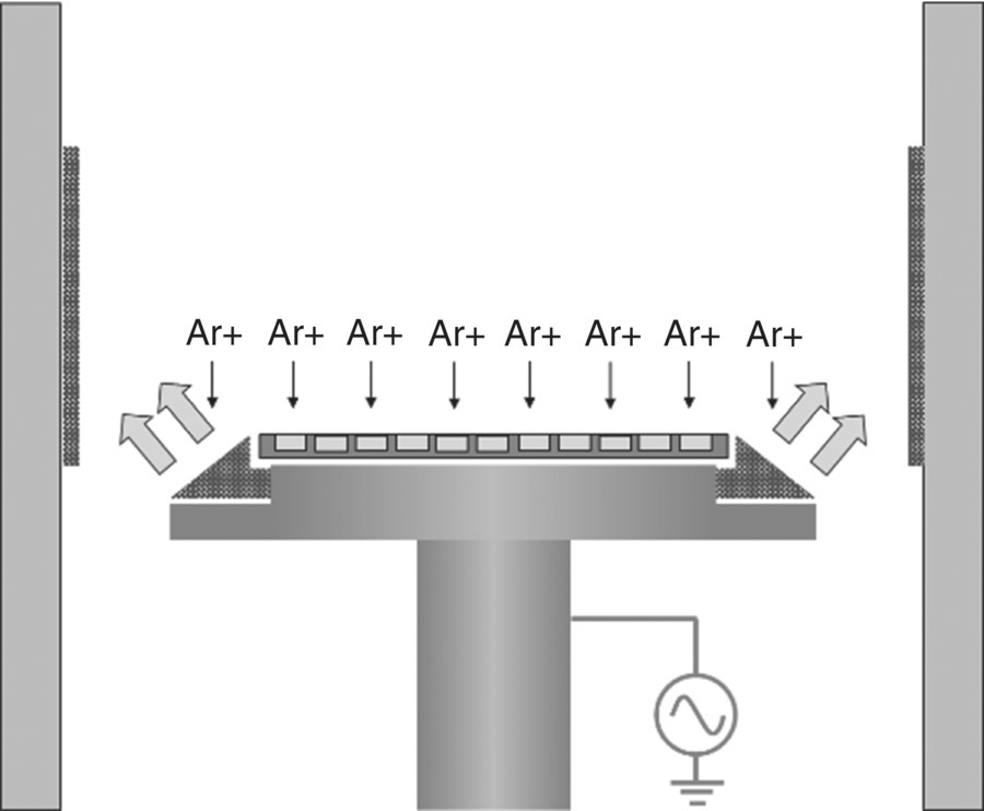
Figure 19.13 In situ pasting during pre‐clean.
Vapor phase decomposition (VPD) analysis during a 5000 wafer marathon showed that the use of this co‐pasting design does not adversely impact contamination levels detected on wafer (Figure 19.14), proving that the concept of sputtering metal away from the wafer is working successfully.

Figure 19.14 VPD metallic contaminant levels using co‐pasting technique.
The co‐pasting concept is compatible with bowed molded wafers and has been optimized to prevent arcing. This solution is now running FO‐WLP production wafers at multiple sites. Co‐pasting increases the wafer‐based pasting interval by >100×, maintaining low particle levels throughout, even at small bin sizes (>0.2 μm) (Figure 19.15).

Figure 19.15 SE‐LTX pre‐clean particle performance with co‐pasting technique employed.
19.4.5 Solution for Rc Management
Common approaches to tackle this problem involve limiting wafer temperature during process, thus reducing the volatility of the C by‐products. Chilled pedestals and chamber furniture are commonplace as a result. In addition to reducing contaminant volatility, vacuum pumping speed is increased to pump away contaminants before they have an opportunity to react with the exposed metal contacts. The use of in situ pasting for particle control reasons can also be used for Rc management purposes, with the co‐pasting technique producing stable Rc performance without the need for frequent wafer pasting (Figure 19.16).

Figure 19.16 RC stability using co‐pasting over 350 wafers with no wafer pasting.
19.4.6 Why Soft ICP Etch Is Best
Given the challenges of large exposed metal and organic material adhesion with ICP ceramic walls, it would be tempting to employ a CCP or diode etch approach to pre‐clean, as the single source concept in the form of a RF‐driven platen allows the chamber walls to be of metal construction. The diode etch approach has several disadvantages however. First, the diode etch concept, being single source, requires relatively high bias voltages to initiate and sustain a plasma discharge (Figure 19.17).

Figure 19.17 ICP vs. diode etch comparison.
Where an ICP etch generates wafer biases in the <500 V range, a diode etch module typically works in bias ranges >3000 V. The higher ion bombardment energy involved produces significantly higher levels of contaminant release from the organic passivation on the wafer. For an equivalent maximum wafer temperature during etch, CO partial pressures can be an order of magnitude higher in a diode etch system compared with ICP. This has obvious implications for Rc.
The high ion energy will also cause a temperature increase that will need additional cool steps given the thermal budget restrictions of molded wafer processing. The cool steps will in turn impact module throughput, assuming the degas throughput bottleneck with an MWD approach has already been solved. With mainstream Si UBM and RDL PVD systems, these problems can be overcome through the use of ESC clamping combined with backside cooling gas to maintain wafer temperatures at low levels, minimizing contaminant volatility. With molded wafer processing, however, ESCs are not reliably compatible because of the excessive wafer bows that can be encountered.
Another disadvantage of diode etch is that etch rate is typically 30–50% of an ICP equivalent, limiting the throughput of the system after the degas bottleneck is addressed.
Finally, the diode etch process is less directional than ICP due to its single source and higher discharge pressures. As CDs reduce the aspect ratio of contact, topography will inevitably increase. For a diode configuration this will mean longer etches are needed to remove native oxide in the base of the contact. Conversely, the ICP etch, being dual source and low pressure (<2 mT), produces an anisotropic etch, directional in nature. As aspect ratios increase, the ICP etch is less affected, and throughputs can be maintained.
19.4.7 Solution for Wafer Warpage
To successfully handle substrates with increased warpages, several aspects of the system design need to be modified. At the atmospheric front end, FOUPs will use 13 slots instead of 25. This enables increased clearances for wafer transfers in and out of FOUPs by the EFEM robot arm. Vertical clearances at the EFEM Aligner and Transport Module Slot Valves are also increased.
Robot arm velocities are adjusted to prevent wafer movement during transfers, and processes are tuned to minimize additional warpage generation caused by excessive temperature change. In addition, optics in front of each process module position are used to detect wafer movement during wafer transfers. Corrective adjustments are then transmitted to the robot arm and applied during the next arm move, recentering the wafer position in time for the next process step. PVD systems have been designed to cope with wafer bows up to 10 mm. Performance has been validated in FO‐WLP production [10].
19.4.8 Solution for Capital Cost Reduction
PVD RDL seed depositions are relatively simple, and for that reason it is important to use hardware that does not exceed requirements. Traditional front‐end‐of‐line (FEOL) PVD chambers used in semiconductor device fabrication facilities are designed to offer features such as high deposition rates, directionality, and advanced uniformity control, which are not critical for FO‐WLP. A basic conventional PVD module will meet the requirements. A picture of a conventional magnetron sputter PVD module is shown in Figure 19.18 and is specifically designed for BEOL processing. The simplicity of the design allows cost savings to be passed on to the user, contributing to the overall task of minimizing the costs to run the FO‐WLP application.

Figure 19.18 SPTS Inspira PVD module for UBM and RDL.
19.5 Additional Equipment Features
In addition to the features already described to deliver productive PVD processing capability, it is worth mentioning an additional technique employed to manage the heat generated by the sputtering process (condensation energy). Si‐based UBM and RDL platforms often take advantage of forced clamping systems with backside gas cooling to limit wafer temperatures, but as explained previously, with highly bowed wafers forced clamping is not always possible. For most the alternative is to use time alone to allow wafers to cool after deposition, but heat transfer is poor at high vacuum so wait times are long, and this has obvious implications for throughput. A more efficient alternative is to use a backfill cool approach.
The backfill cool technique is similar to clamping in that argon is used to conduct heat away from the wafer to a relatively cold platen beneath, except with backfills; no clamping is involved (Figure 19.19). The procedure involves isolating the vacuum pump temporarily, filling the chamber with argon to reach ~1 T, pausing while heat is transferred away from the wafer, then opening the vacuum line, pumping the argon away, and commencing sputtering.

Figure 19.19 Backfill cool concept for bowed wafer cooling.
Backfill process times and insertion points in the process flow are coordinated to maximize system throughput, working within defined thermal budget restrictions of the process.
19.6 Design Rules Related to the Equipment
As previously described, PVD systems need to be able to cope with wafer bows up to the 10 mm range to fully accommodate the variety of FO‐WLP process flows and die combinations in use. Mold thickness is generally in the 500–1000 μm range, but it is warpage that limits the PVD system capability rather than the thickness. Obviously the two can be interrelated.
Wafers in the 200–330 mm range can be processed. The use of conventional PVD chambers with relatively short target to wafer spacing (~50 mm) means that designs with low topography can be processed successfully (e.g. vias with aspect ratios up to the 1–1.5 : 1 range). Given that most structures have 20–50 μm CD and 5–10 μm passivation thickness, this means conventional PVD falls safely within the operating range.
For those with an interest in depositing PVD seeds for through‐mold via (TMV) purposes, alternative PVD chamber hardware is available [8]. Ionized PVD is used whereby material not only is sputtered from the target but is also ionized. By applying a DC bias to the wafer, sputtered metal ions are attracted and accelerated toward the wafer, driving the material with a more vertical component of direction down into high aspect ratio vias. With additional DC bias applied, the material in the base of the vias can be re‐sputtered onto the sidewalls, providing a conducting path for an ECD process to fill the TMV with conducting material such as Cu (Figure 19.20).

Figure 19.20 Continuous Cu in through‐mold via test structures.
Depositing a metal liner into a TMV created by laser drilling is challenging because of the roughness of the via sidewalls – much rougher than anything produced with the more traditional Si‐based TSV structures plasma etched using Bosch or equivalent etch techniques. Despite this, with enough material deposited in the field, ionized PVD has been shown to produce sufficient coverage for plating [9]. The challenge comes more from managing the thermal effects of working with an ionized metal plasma reactor when temperature‐sensitive materials are involved.
19.7 Reliability
The data in Figure 19.21 illustrates the reliability of current generation PVD tools for FO‐WLP production [10].

Figure 19.21 FO‐WLP PVD system reliability data.
The data shows that systems processing warped FO‐WLP wafers involving mixed die combinations (in some cases warping up to 7–8 mm for substrates >300 mm diameter) can operate with uptimes >90%. Breakage rates that are <1 in 70k have been reported, in line with mainstream silicon PVD system performance.
From a device performance perspective, Figure 19.22 shows Rc values collected over a six‐month period (approximately 5000 measurements, 35 μm CD test structures, PI passivation). Low Rc values <2 mΩ are achieved and maintained throughout the monitoring period.

Figure 19.22 FO‐WLP device test structure Rc repeatability.
19.8 Next Steps
Aside from the potential introduction of ionized PVD for higher aspect ratio features, FO‐WLP PVD developments will continue to focus on Rc management and cost reduction. For Rc management, new pre‐clean chamber designs will emerge with continued emphasis on contamination prevention or rapid removal.
Cost reduction is a continuous process, so it will be on any FO‐WLP production roadmap. Improvements in mechanical throughput are anticipated with the development of faster robot arm systems from the robotics OEMs. This is most likely to impact high‐end RDL‐first process flows that run with reduced bow substrates and higher transfer speeds.
For degas performance it is anticipated that reduced cost passivation and mold materials will continue to emerge, some with higher temperature tolerances, but with potentially worse outgassing behavior. MWD temperature capability should be in place to address this.
For incoming wafer conditions, bow values are expected to increase as material reduction takes place from efforts to reduce costs as well as thinner molded wafers for low profile packages (<500 μm). This will put more demands on the PVD systems as well as equipment and materials for the entire FO‐WLP process flow, especially those running on larger wafer sizes. Adoption of larger and more diverse combinations of SIP configurations will also lead to higher warpages – and with SIP being one of the most popular emerging package types for FO‐WLP, this is sure to drive the average warpage values up.
Currently, there is a lot of research in the area of panel‐level fan‐out [11]. It is clear that there might be a place for panel‐level fan‐out with low density packages, provided identified technical roadblocks through the process flow are overcome, but the high performance packages using high density RDL will almost certainly remain wafer based largely because of the lithography limitations encountered with large bowed panel processing. Return on investment (RoI) arguments for developing a panel‐based equivalent PVD system are not compelling today [12].
References
- 1 Brunnbauer, M., Furgut, E., Beer, G. et al. (2006). An embedded device technology based on a molded reconfigured wafer. Proceedings of the 56th Electronics Components and Technology Conference (ECTC 2006), San Diego, USA, pp. 448–551.
- 2 Brunnbauer, M., Fürgut, E., Beer, G., and Meyer, T. (2008). Embedded wafer level ball grid array (eWLB). Proceedings of the 10th Electronics Packaging Technology Conference (EPTC 2008), Singapore, pp. 994–998.
- 3 Wasa, K. and Hayakawa, S. (1992). Thin film processes. In: Handbook of Sputter Deposition Technology, chapter 2, 2–48. NJ, USA: Noyes Publications.
- 4 Thornton, J. (1974). Influence of apparatus geometry and deposition conditions on the structure and topography of thick sputtered coatings. Journal of Vacuum Science and Technology 11: 666–670.
- 5 Jones, C., Butler, D., and Burgess, S. (2016). High productivity UBM/RDL deposition by PVD for FO‐WLP applications. Proceedings of the International Wafer Level Packaging Conference (IWLPC 2016), San Jose, USA.
- 6 Jones, C. (2013). Cost‐effective & productive PVD for Advanced Packaging UBM/RDL with Sigma fxP. Presented at SEMICON Taiwan 2013 Advanced Packaging Workshop, Taipei, Taiwan.
- 7 Knight, N., Burgess, S., Jones, C. et al. (2017). Rc management for next generation PVD UBM/RDL metallization schemes. Proceedings of the International Wafer Level Packaging Conference (IWLPC 2017), San Jose, USA.
- 8 Urbansky, N., Burgess, S.R., Schmidbauer, S. et al. (2002). Advanced hi‐fill® for interconnect liner applications. Microelectronic Engineering Vol. 64: 99–105.
- 9 Butler, D. (2015). High density packaging on wafer level fan‐out: deposition and via drilling solutions tailored for non‐silicon substrates. Presented at SEMI European 3D Summit 2015, Grenoble, France.
- 10 Vishwanath, S. (2016). Achieving high quality and low cost PVD – critical for success in advanced packaging. Presented at SEMI Taiwan WLCSP Equipment Technology Forum, Taipei, Taiwan (June 2016).
- 11 Werbaneth, P. (October 2016), “First‐Mover Advantage: Fan‐Out Panel Level Packaging at IWLPC 2016”, 3DInCites [Online]. https://www.3dincites.com/2016/10/first‐mover‐advantage‐fan‐out‐panel‐level‐packaging‐at‐iwlpc‐2016 (accessed 6 August 2018).
- 12 I‐Micronews (July 2017). Inside PVD Technology for Fan‐Out by SPTS, Yole Development [Online]. https://www.i‐micronews.com/news/advanced‐packaging/9596‐inside‐pvd‐technology‐for‐fan‐out‐by‐spts.html (accessed 6 August 2018).