
1.7 A FIRST EXAMPLE
Common examples of application fields resorting to embedded solutions are cryptography, access control, smart cards, automotive, avionics, space, entertainment, and electronic sales outlets. In order to illustrate the main steps of the design process, a small digital signature system will now be developed (complete assembly language and VHDL code available).
1.7.1 Specification
The system under development (Figure 1.1) has three inputs,
- character is an 8-bit vector.
- new_character is a signal used for synchronizing the input of successive characters.
- sign is a control signal ordering the computation of a digital signature.
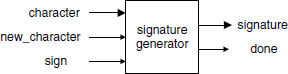
and two outputs,
- done is a status variable indicating that the signature computation has been completed,
- signature is a 32-bit vector, namely, the signature of the message.
The working of the system is shown in Figure 1.2: a sequence c1, c2, … , cn of any number n of characters (the message), synchronized by the signal new_character, is inputted. When the sign control signal goes high, the done flag is lowered and the signature of the message is computed. The done flag will be raised as soon as the signature s is available.
In order to sign the message two functions must be defined:
- a hash function associating a 32-bit vector (the summary) to every message, whatever its length;
- an encode function computing the signature corresponding to the summary.
The following (naive) hash function is used:
Algorithm 1.1 Hash Function
summary:=0;
while not(end_of_message) loop
    get(character);
    a:=(summary(7 downto 0)+character) mod 256;
    summary(23 downto 16):=summary(31 downto 24);
    summary(15 downto 8):=summary(23 downto 16);
    summary(7 downto 0):=summary(15 downto 8);
    summary(31 downto 24):=a;
end loop;

Figure 1.2 Input and output signals.
As an example, assume that the message is the following (every character can be equivalently considered as an 8-bit vector or a natural number smaller than 256, i.e. a base-256 digit; see Chapter 3):
![]()
The summary is computed as follows:

The final result, translated from the base-256 to the decimal representation, is
![]()
The encode function computes
![]()
x being some private key, and m a 32-bit number. Assume that
Then the signature of the previous message is
![]()
1.7.2 Number Representation
In this example all the data are either 8-bit vectors (the characters) or 32-bit vectors (the summary, the key, and the module m). So instead of representing them in the decimal numeration system, they should be represented in the binary or, equivalently, the hexadecimal system. The message is
![]()
The summary, the key, the module, and the signature are

1.7.3 Algorithms
The hash function amounts to a mod-256 addition, that is, a simple 8-bit addition without output carry. The only complex operation is the mod m exponentiation.
Assume that x, y, and m are n-bit numbers. Then
![]()
and e can be written in the form
![]()
The corresponding algorithm is the following (Chapter 8, Algorithm 8.14).
Algorithm 1.2 Exponentiation
e:=1;
for i in 1..n loop
   e:=(e*e) mod m;
   if x(n-i)=1 then e:=(e*y) mod m; end if;
end loop;
The only computation primitive is the modulo m product, which, in turn, is equivalent to a natural multiplication followed by a modulo m reduction, that is, an integer division by m. The following algorithm (Chapter 8, Algorithm 8.5) computes r = x.y mod m. It uses two procedures: multiply, which computes the product z of two natural numbers x and y, and divide, which generates q (the quotient) and r (the remainder) such that z = q.m + r with r < m.
Algorithm 1.3 Modulo m Multiplication
multiply (x, y, z);
divide (z, m, q, r);
A classical method for computing the product z of two natural numbers x and y is the shift and add algorithm (Chapter 5, Algorithm 5.3). In base 2:
Algorithm 1.4 Natural Multiplication
p(0):=0;
for i in 0..n−1 loop
     p(i+1):=(p(i)+x(i)*y)/2;
end loop;
z:=p(n)*(2**n);
For computing q and r such that z = q.m + r with r < m, the classical restoring division algorithm can be used (Chapter 6, Algorithms 6.1 and 6.2). Given x and y (the operands) such that x < y, and p (the desired precision), the restoring division algorithm computes q and r such that
Within the exponentiation algorithm 1.2, the operands e and y are n-bit numbers. Furthermore, e is always smaller than m, so that both products z = e * e or z = e * y are 2.n-bit numbers satisfying the relation
![]()
Thus by substituting x by z, p by n, and y by m.2n in (1.1), the restoring division algorithm computes q and r′ such that
![]()
that is,
![]()
The restoring algorithm is similar to the pencil and paper method. At every step the latest obtained remainder, say, r(i − 1), is multiplied by 2 and compared with the divider y. If 2.r(i − 1) is greater than or equal to y, then the new remainder is r(i) = 2.r(i − 1) − y and the corresponding quotient bit is equal to 1. In the contrary case, the new remainder is r(i) = 2.r(i − 1) and the corresponding quotient bit equal to 0. The initial remainder r(0) is the dividend.
Algorithm 1.5 Restoring Division
r(0):=z; y:=m*(2**n);
for i in 1.. n loop
   if 2*r(i−1)−y<0 then q(i):=0; r(i):=2*r(i−1); else
   q(i):=1; r(i):=2*r(i−1)−y; end if;
end loop;
r:=r(n)/(2**n);
By merging Algorithms 1.4 and 1.5, the following modular product algorithm is obtained.
Algorithm 1.6 Modular Product
p(0):=0;
for i in 0..n−1 loop
   p(i+1):=(p(i)+x(i)*y)/2;
end loop;
r(0):=p(n)*(2**n); y:=m*(2**n);
for i in 1.. n loop
   if 2*r(i-1)-y<0 then q(i):=0; r(i):=2*r(i-1); else
   q(i):=1; r(i):=2*r(i-1)-y; end if;
end loop;
r:=r(n)/(2**n);
Observe that the multiplication of p(n) and m by 2n, as well as the division of r(n) by 2n can be deleted. Then r(0) = p(n) is a 2.n-bit fixed-point number (Chapter 3) smaller than 2n and the divider is equal to m. The quotient q and the remainder r(n) satisfy the relation p(n).2n = q.m + r(n) so that r = r(n).
1.7.4 Hardware Platform
For implementing this illustrative example, a prototyping board will be used, namely, an XSA-100 board from XESS Corporation. It includes an XC2S100 FPGA (Spartan-II family of Xilinx) integrating the complete digital signature system. The design environment includes virtual components (synthesizable VHDL models, Chapter 9), among others PicoBlaze, an 8-bit microprocessor, and its program memory ([XIL2002]).
1.7.5 Hardware–Software Partitioning
As mentioned above, the only complex operation is the computation of yx modulo m. All the other operations can be carried out by the processor. The corresponding system architecture is shown in Figure 1.3. It works as follows:

Figure 1.3 System architecture.
- PicoBlaze reads the character input at address 0 and the command input at address 1, where
command= 0 0 0 0 0 0 sign new_character.
- It computes the 32-bit summary and writes it, under the form of four separate bytes,
into four registers whose addresses are 3, 2, 1 and 0, respectively.
summary = Y(3) Y(2) Y(1) Y(0),
- A specific coprocessor receives the start signal from PicoBlaze at address 4, computes
s = (summary) 737FD3F9 mod FFFFFFFF,and generates the done flag.
1.7.6 Program Generation
The program executed by PicoBlaze is made up of three parts (assembly language code available):
- reading of the new_character and sign input signals,
- reading of the character input and updating of the summary,
- writing of the summary and of the start command within the interface registers:
summary:=(0, 0, 0, 0);
start:=0;
loop
    --wait for command=0
    while command>0 loop null; end loop;
    --wait for command=1 (new_character) or 2 (sign)
    while command=0 loop null; end loop;
    if command=1 then
      a:=(summary(0)+character) mod 256;
      summary(0):=summary(1);
      summary(1):=summary(2);
      summary(2):=summary(3);
      summary(3):=a;
    elsif command=2 then
      Y(3):=summary(3);
      Y(2):=summary(2);
      Y(1):=summary(1);
      Y(0):=summary(0);
      start:=1;
      summary:=(0, 0, 0, 0);
     start:=0;
    end if;
end loop;
1.7.7 Synthesis
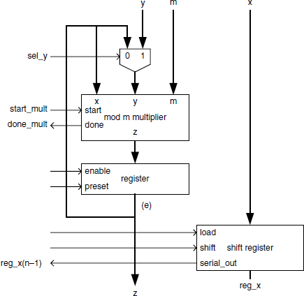
The synthesis (complete VHDL code available) of the exponentiator block of Figure 1.3 is based on the algorithms of Section 1.7.3. A summary of the main principles for translating an algorithm to a circuit is given in Chapter 10. The data path of Figure 1.4 allows executing Algorithm 1.2. It includes:
- two 32-bit registers: a parallel register storing e, and a loadable shift register, initially storing x and allowing to successively read the value of x(n − 1), x(n − 2), … , x(0);
- a mod m multiplier with a start input signal and a done output flag;
- a 32-bit 2-to-1 multiplexer selecting either e or y as the second multiplier operand.
The complete circuit is described by the following VHDL model (including the control unit):
entity exponentiator is
port  (
    x, y, m: in std_logic_vector(n−1 downto 0);
    z: inout std_logic_vector(n−1 downto 0);
    clk, reset, start: in std_logic;
    done: out std_logic
);
end exponentiator;
architecture circuit of exponentiator is
  component sequential_mod_mult..end component;
  signal start_mult, sel_y, done_mult: std_logic;
  signal reg_x, input_y, output_z: std_logic_vector(n−1 downto
  0);
  subtype step_number is natural range 0 to n;
  signal count: step_number;
  subtype internal_states is natural range 0 to 14;
  signal state: internal_states;
begin
  label_1: sequential_mod_mult port map(z, input_y, m,
  output_z, clk, reset, start_mult, done_mult);
  with sel_y select input_y<=z when ‘0’, y when others;
  process (clk, reset)
  begin
    if reset=‘1’ then
       state<=0; done<=‘0’; start_mult<=‘0’; count<=0;
    elsif clk’event and clk=‘1’ then
      case state is
          when 0=>if start=‘0’ then state<=state+1; end if;
          when 1=>if start=‘1’ then state<=state+1; end if;
          when 2=>z<=conv_std_logic_vector(1, n);
            reg_x<=x; count<=0; done<=‘0’; state<=state+1;
          when 3=>
            sel_y<=‘0’; start_mult<=‘1’; state<=state+1;
          when 4=>state<=state+1;
          when 5=>start_mult<=‘0’; state<=state+1;
          when 6=>
            if done_mult=‘1’ then state<=state+1; end if;
          when 7=>z<=output_z;
            if reg_x(n−1)=‘1’ then state<=state+1;
            else state<=13; end if;
          when 8=>
            sel_y<=‘1’; start_mult<=‘1’; state<=state+1;
          when 9=>state<=state+1;
          when 10=>start_mult<=‘0’; state<=state+1;
          when 11=>
            if done_mult=‘1’ then state<=state+1; end if;
          when 12=>z<=output_z; state<=state+1;
          when 13=>reg_x(0)<=reg_x(n−1);
            for i in 1 to n−1 loop reg_x(i)<=reg_x(i-1);
            end loop;
            count<=count+1; state<=state+1;
          when 14=>
            if count>=n then done<=‘1’; state<=0;
            else state<=3; end if;
        end case;
      end if;
    end process;
end circuit;
1.7.8 Prototype
All the files (complete source files available) necessary for programming an XSA-100 board are included in the file section1_7.zip:
- exponentiator.vhd is the complete description of the exponentiation circuit (including the modular multiplier model);
- signatu.psm is the assembly language program;
- kpcsm.vhd is the PicoBlaze model;
- signatu.vhd is the program memory model generated from the assembly language program with kcpsm.exe (the PicoBlaze assembler released by Xilinx [XIL2002]).
In order to test the complete system, the circuit of Figure 1.5 has been synthesized. It is made up of:
- the circuit of Figure 1.3 including PicoBlaze, its program memory, the interface registers, and the exponentiator;
- a finite state machine generating the commands and characters corresponding to the example of Section 1.7.1;
- a circuit that interfaces the board with signals d(7..0) controllable from the host computer ([XSA2002]):
- d(7) cannot be used,
- d(3..0) are used for selecting one of the outputs (out_0 to out_15) or inputs (in_0 to in_15),
- d(6..4) are control signals,
d(6.4) Command 000 nop 001 write 010 read 011 reset 100 address strobe
in this application the write and address strobe commands are not used; when the read command is active, the hexadecimal representation of the 4-bit vector selected with d(3..0) is displayed on the LED of the board;
- the 7-segment LED decoder.
The VHDL model of the circuit of Figure 1.5 (firma.vhd) is also included in section1_7.zip as well as the file describing the pin assignment (pines.ucf). The whole system (Figure 1.5) can be synthesized with ISE, the synthesis program of Xilinx, and downloaded to the XSA-100 board.