13.2 INTEGERS
13.2.1 Base-2 Nonrestoring Divider
Let Y be an n-bit positive number and X an integer belonging to the range − Y ≤ X < Y, so that it can be represented as an (n + 1)-bit 2's complement number. The circuit corresponding to the nonrestoring algorithm 6.6 (with q(i) substituted by q(p − i) in order that the least significant bit of q be q(0)) is shown in Figures 13.6 (basic cell), 13.7 (divider structure, combinational and sequential implementations), and 13.8 (correction circuit).
The cost and computation time of the corresponding divider are
and
Examples 13.4 (Complete VHDL source code available.) Generate a VHDL model of a generic base-2 nonrestoring divider (Figures 13.6, 13.7, and 13.8):
entity nonr_cell is
port (
  a: in STD_LOGIC_VECTOR (N-1 downto 0);
  b: in STD_LOGIC_VECTOR (N-1 downto 0);
  q: in STD_LOGIC;
  r: out STD_LOGIC_VECTOR (N downto 0)
);
end nonr_cell;

architecture nr_cel_arch of nonr_cell is
signal a_by_2: STD_LOGIC_VECTOR (N downto 0);
begin
a_by_2<=a(N-1 downto 0)&‘0’;
adder_subtracter: process (a_by_2,b,q)
begin
  if q=‘1’ then r<=a_by_2+b;
  else r<=a_by_2 - b;
  end if;
end process;
end nr_cel_arch;

Figure 13.6 Nonrestoring divider: basic cell.

Figure 13.7 Nonrestoring divider: general structure.
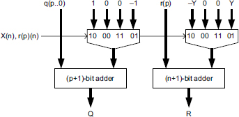
Figure 13.8 Nonrestoring divider: correction circuit.
The final correction circuit of Figure 13.8 is:
entity correction_cell is
port (
  Q: in std_logic_vector(P downto 0);
  R: in std_logic_vector(N downto 0);
  Y: in std_logic_vector(N-1 downto 0);
  x_n: in std_logic;
  r_n: in std_logic;
  adj_Q: out std_logic_vector(P downto 0);
  adj_R: out std_logic_vector(N downto 0)
);
end correction_cell;

architecture correction_arch of correction_cell is
signal selector: std_logic_vector(1 downto 0);
begin
  selector<=x_n&r_n;
  correction: process (selector,Q,R,Y)
  begin
    case selector is
      when “10”=>adj_Q<=Q+1; adj_R<=R - Y;
      when “01”=>adj_Q<=Q-1; adj_R<=R+Y;
      when others=>adj_Q<=Q; adj_R<=R;
  end case;
end process;
end correction_arch;
entity div_nr is
port (
  X: in STD_LOGIC_VECTOR (N downto 0);
  Y: in STD_LOGIC_VECTOR (N-1 downto 0);
  Q: out STD_LOGIC_VECTOR (P downto 0);
  R: out STD_LOGIC_VECTOR (N downto 0)
);
end div_nr;

architecture div_arch of div_nr is
type connect is array (0 to P) of STD_LOGIC_VECTOR (N downto 0);
Signal wires: connect;
Signal QQ: STD_LOGIC_VECTOR (P downto 0);
begin
  wires(0)<=X;
  divisor: for i in 0 to P-1 generate
  nr_step: nonr_cell port map (wires(i)(N-1 downto 0),
  Y, wires(i)(N), wires(i+1));
  end generate;

  QQ(P)<=wires(0)(N);
  Quotient: for i in 1 to P-1 generate
    QQ(P-i)<=not wires(i)(N);
  end generate;
  QQ(0)<=‘1’;
  final_adjust: correction_cell port map (QQ(P downto 0),
  wires(P), Y, X(N), wires(P)(N), Q, R);
end div_arch;
Given two n-bit normalized numbers, that is, two natural numbers X and Y such that
![]()
synthesize a circuit generating the quotient Q and the remainder R with an accuracy of p bits, that is,
![]()
In order that the dividend be smaller than the divider, X is substituted by X/2 < 2n−1 ≤ Y. According to Comment 6.3, it's only a matter of defining 2.r(0) = X (instead of 2.X) and performing the division with an accuracy of p + 1 bits. The corresponding iterative circuit is shown in Figure 13.9. The final correction circuit is simpler: X is positive so that, in Figure 13.8, X(n) = 0.

Figure 13.9 Divider for normalized numbers.
Example 13.5 (Complete VHDL source code available.) Generate the VHDL model of a divider for normalized base-2 numbers (Figure 13.9 with the basic cell of Figure 13.6):
entity nr_cell is
port (
  a_by_2: in STD_LOGIC_VECTOR (N downto 0);
  b: in STD_LOGIC_VECTOR (N-1 downto 0);
  q: in STD_LOGIC;
  r: out STD_LOGIC_VECTOR (N downto 0)
);
end nr_cell;

architecture nr_cel_arch of nr_cell is
begin
adder_subtracter: process (q,a_by_2,b)
begin
  if q=‘1’ then r<=a_by_2+b;
  else r<=a_by_2 - b;
  end if;
end process;
end nr_cel_arch;
The correction cell of Figure 13.8 (if necessary) is reduced to a conditional adder, and the last quotient bit (q(0)) is the negative of the last-remainder's most-significant-bit.
entity cond_adder is
port (
  a: in STD_LOGIC_VECTOR (N-1 downto 0);
  b: in STD_LOGIC_VECTOR (N-1 downto 0);
  sel: in STD_LOGIC;
  r: out STD_LOGIC_VECTOR (N-1 downto 0)
);
end cond_adder;
architecture cond_adder_arch of cond_adder is
begin
  conditional_adder: process (sel,a,b)
  begin
    if sel=‘1’ then r<=a+b;
    else r<=a;
    end if;
end process;
The divider structure of Figure 13.9 is:
entity div_nr_norm is
port (
  X: in STD_LOGIC_VECTOR (N-1 downto 0);
  Y: in STD_LOGIC_VECTOR (N-1 downto 0);
  Q: out STD_LOGIC_VECTOR (P-1 downto 0);
  R: out STD_LOGIC_VECTOR (N-1 downto 0)
);
end div_nr_norm;

architecture div_arch of div_nr_norm is
type connect is array (0 to P+1) of STD_LOGIC_VECTOR (N
downto 0); Signal r_in, r_out: connect;
Signal op: STD_LOGIC_VECTOR (P+1 downto 0);
begin
  wires_in(0)<=‘0’&X; op(0)<=‘0’;
  divisor: for i in 0 to P generate
    nr_step: nr_cell port map (r_in(i), b=>Y, op(i), r_out(i));
    Q(P-i)<=not wires_out(i)(N); op(i+1)<=r_out(i)(N);
    r_in(i+1)<=r_out(i)(N-1 downto 0)&‘0’;
  end generate;
  rem_adj: cond_adder port map (r_out(P)(N-1 downto 0),
  Y, r_out(P)(N), R);
end div_arch;
13.2.2 Base-B Nonrestoring Divider
Figure 13.10 depicts the basic cell corresponding to the non restoring base-B division step of Algorithm 6.10. It includes an 8-input 2-output look-up table (LUT), a 2-digit by n-digit multiplier, and an (n + 2)-digit subtractor. The LUT inputs are rt, entered as the five leftmost digits B.r(i)(n + 1..n − 3) of the shifted remainder, and Yt, entered as the three leftmost digits Y(n − 1..n − 3) of the divisor; the 2-digit output corresponds to the result qt of the integer division rt/Yt + 1, namely the selected 2-digit quotient.
The LUT size and cost can become prohibitive for increasing values of B, so a fast 5-digit by 3-digit base-B divider can be designed as an alternative. The multiplier output is the product qt.Y of the selected quotient by the divisor. According to the resources at hand those products may be precalculated then stored for fast retrieval. The subtractor computes the new remainder as the difference B.r(i) − qt.Y. Finally, a carry-save computation of r(i + 1) could be implemented but conditions over the quotient-digit set have to be relaxed. The divider structure is shown in Figure 13.11.
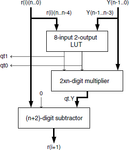
Figure 13.10 Base-B nonrestoring divider: basic cell.
The cost and computation time of the nonrestoring divider basic cell of Figure 13.10 are given by
and
or
if carry-save is implemented.

Figure 13.11 Nonrestoring base-B divider: general structure.
The cost and computation time of the non restoring base-B divider of Figure 13.11 are given by
and
Example 13.6 (Complete VHDL source code available.) Generate a generic n-digit base-B nonrestoring divider. The division step of Figure 13.10 is:
entity nr_baseB_step is
port (
  a: in digit_vector(N downto 0);
  b: in digit_vector(N-1 downto 0);
  q1, q0: out digit;
  r: out digit_vector(N downto 0)
);
end nr_baseB_step;

architecture behavioral of nr_baseB_step is
signal rt: digit_vector(4 downto 0);
signal yt: digit_vector(2 downto 0);
signal qt1,qt0: digit;
signal a_x_BASE, q_x_b, remainder: digit_vector(N downto 0);

begin
  rt<=a(N downto N-4);
  yt<=b(N-1 downto N-3);
  a_x_BASE(N downto 1)<=a(N-1 downto 0); a_x_BASE(0)<=0;
  LookUpTable:look_up_table port map (rt, yt, qt1, qt0);
  mult: base_b_2_x_n_mult port map (qt1&qt0, B, q_x_b);
  subtractor: base_b_subt port map (a_x_BASE, q_x_b, remainder);
  q1<=qt1; q0<=qt0;
  r<=remainder;
end behavioral;
The divider structure is:
entity div_nr_baseB is
port (
  A: in digit_vector(N-1 downto 0);
  B: in digit_vector(N-1 downto 0);
  Q: out digit_vector(P-1 downto 0);
  R: out digit_vector(N-1 downto 0)
);
end div_nr_baseB;

architecture div_arch of div_nr_baseB is
type connections is array (0 to P) of digit_vector(N downto 0);
Signal wires: connections;
signal Q_1, Q_0: digit_vector(P downto 0);
begin
  wires(0)<=0&A;
  divisor: for i in 0 to P-1 generate
    rest_step: nr_baseB_step port map (wires(i), B,
    Q_1(P-i), Q_0(P-i-1), wires(i+1));
  end generate;
  correction: rem_adjust port map (wires(P), B, Q_1(0), R);
  final_adder: base_B_adder port map (Q_1(P-1 downto 0),
               Q_0(P-1 downto 0), Q);
end div_arch;
13.2.3 SRT Dividers
13.2.3.1 SRT-2 Divider
The SRT-2 divider with full computation of the remainder will be presented first. Let Y be an n-bit normalized number (Example 6.4.2) and X an n-bit 2's complement integer, that is,
![]()
Then Algorithm 6.7 (with q(i) substituted by q(p − i) in order that the least significant bit of q be q(0)) can be applied. At each step the following operation is performed:
![]()
where r(i + 1) and r(i) are n-bit 2's complement numbers, and Y an n-bit natural and q(p − i − 1) a signed bit (−1, 0 or 1) whose value is defined (Table 6.1) as a function of w(n) and w(n − 1), that is, r(i)(n − 1) and r(i)(n − 2).
The basic cell is shown in Figure 13.12. If en = 0, then r = a_by_2; if en = 1 then r = a_by_2 ± b where the operation is selected by op (0: add; 1: subtract). The divider structure is shown in Figure 13.13. The combinational circuit implements Table 13.1. Observe that op(p-i-1) can be chosen equal to q_pos(p-i-1), so that it is a 2-input 3-input combinational circuit. An additional (not represented) (p + 1)-bit subtractor generates Q = q_pos-q_neg. Furthermore, a correction circuit, similar to that of Figure 13.8, is necessary if the condition sign(R) = sign(X) must hold.
The cost and computation time of the non restoring divider basic cell of Figure 13.12 are given by
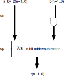
Figure 13.12 SRT-2 divider: basic cell.
and
The cost and computation time of a nonrestoring SRT-2 divider (Figure 13.13 with an additional (p + 1)-bit subtractor for computing q_pos-q_neg), without the correction circuit, are given by
and
where CLUT(2, 3) and TLUT(2, 3) are the cost and computation time of a 2-input 3-output combinational circuit (e.g., a look-up table).
Comment 13.1 The SRT-2 algorithm is very similar to the base-2 nonrestoring algorithm. The latter is based on the diagram of Figure 6.4b while the former is based on the diagram of Figure 6.3b. At the circuit level, the similarity is quite evident: compare Figures 13.7 (nonrestoring) and 13.13 (SRT-2), taking into account that in the first case X is an (n + 1)-bit 2's complement number and in the second case an n-bit 2's complement number. The difference is that the SRT-2 method needs a 2-input table in order to select the next quotient bit value, while the nonrestoring algorithm only needs a 1-bit table (an inverter). Furthermore, the SRT-2 circuit needs an additional output subtractor, or some kind of on-the-fly conversion circuit. As regards the cost and computation time, the nonrestoring method should always be better than (or equivalent to) the SRT-2 method. The real advantage of the base-2 SRT algorithm is when stored-carry encoding is used (next section).

Figure 13.13 SRT-2 divider: general structure.
TABLE 13.1 Selection of q_pos(p-i-1), q_neg(p--i-1),en(p-i-1), and op(p-i-1)

Example 13.7 (Complete VHDL source code available.) Generate a generic n-bits base-2 SRT divider. The division step of Figure 13.12 is:
entity srt_cell is
port (
  r_by_2: in STD_LOGIC_VECTOR (N-1 downto 0);
  y: in STD_LOGIC_VECTOR (N-1 downto 0);
  en, op: in STD_LOGIC;
  r_n: out STD_LOGIC_VECTOR (N-1 downto 0)
);
end srt_cell;
architecture behavioral of srt_cell is
begin
  cell: process (en,op,y,r_by_2)
  begin
    if en=‘1’ then
     if op=‘1’ then r_n<=r_by_2-y;
     else r_n<=r_by_2+y;
     end if;
    else r_n<=r_by_2;
    end if;
  end process;
end behavioral;
The combinational circuit of Table 13.1 is:
entity comb_circ is
port (
  r: in STD_LOGIC_VECTOR (1 downto 0);
  q_pos, q_neg: out STD_LOGIC;
  en, op: out STD_LOGIC);
end comb_circ;

architecture behavioral of comb_circ is
begin
 combinational: process (r)
 begin
   case r is
     when “00”=>q_pos<=‘0’; q_neg<=‘0’; en<=‘0’; op<=‘-’;
     when “01”=>q_pos<=‘1’; q_neg<=‘0’; en<=‘1’; op<=‘1’;
     when “10”=>q_pos<=‘0’; q_neg<=‘1’; en<=‘1’; op<=‘0’;
     when “11”=>q_pos<=‘0’; q_neg<=‘0’; en<=‘0’; op<=‘-’;
     when others=>NULL;
  end case;
end process;
end behavioral;
The divider structure of Figure 13.13 is:
entity SRT_radix2 is
port (
  X: in STD_LOGIC_VECTOR (N-1 downto 0);
  Y: in STD_LOGIC_VECTOR (N-1 downto 0);
  Q: out STD_LOGIC_VECTOR (P downto 0);
  R: out STD_LOGIC_VECTOR (N-1 downto 0)
);
end SRT_radix2;

architecture srt_arch of SRT_radix2 is
type connect is array (0 to P) of STD_LOGIC_VECTOR (N downto 0);
signal r_in, r_out: connect;
signal QQ, Q_pos, Q_neg, en, op: STD_LOGIC_VECTOR (P downto 0);
begin
  r_in(0)<=X&‘0’;
  divisor: for i in 0 to P-1 generate
   comb: comb_circ port map(r_in(i)(N downto N-1),
       Q_pos(P-i-1), Q_neg(P-i-1), en(P-i-1), op(P-i-1));
  div_step: srt_cell port map (r_in(i)(N-1 downto 0), Y,
         en(P-i-1), op(P-i-1),r_out(i)(N-1 downto 0));
  r_in(i+1)<=r_out(i)(N-1 downto 0)&‘0’;
 end generate;
 QQ<=(‘0’&Q_pos) - (‘0’&Q_neg);
 final_adjust: correction_cell port map (QQ, r_in(P)(N downto 1),
Y, x_n=>X(N-1), r_in(P)(N), Q, R);
end srt_arch;
13.2.3.2 SRT-2 Divider with Carry-Save Computation of the Remainder
Let Y be an n-bit normalized number and X an integer belonging to the range − Y ≤ X < Y, so that it can be expressed as an (n + 1)-bit 2's complement integer. Then Algorithm 6.8 can be applied. At each step the following operation is performed (recall that s′ and c′ stand for s/2 and c/2):
![]()
where s′(i + 1), c′(i + 1), s′(i), and c′(i) are (n + 2)-bit 2's complement numbers, Y is an n-bit natural number, and q(p − i − 1) is a signed bit (− 1, 0 or 1) whose value is defined (Figure 6.5 and Table 6.2) as a function of s(i)(n + 2..n − 1) and c(i)(n + 2..n − 1), that is, s′(i)(n + 1..n − 2) and c′(i)(n + 1..n − 2).
The basic cell is shown in Figure 13.14. The carry-save adder is a set of full adders working in parallel (Chapter 11), so that its computation time does not depend on the operand size. If en = 0, then ![]() c′(i)); if en = 1 then
c′(i)); if en = 1 then ![]() where the operation is selected by op (0: add; 1: subtract). The divider structure is shown in Figure 13.16. The combinational circuit (Figure 13.15) implements the circuit of Table 13.2. An additional (not represented) p-bit subtractor generates Q = q_pos − q_neg. Another additional (not represented) (n + 1)-bit adder generates r(p) = s′(p) + c′(p), that is, the decoded value of the final remainder. Furthermore, a correction circuit, similar to that of Figure 13.6, is necessary if the condition sign(R) = sign(X) is to hold.
where the operation is selected by op (0: add; 1: subtract). The divider structure is shown in Figure 13.16. The combinational circuit (Figure 13.15) implements the circuit of Table 13.2. An additional (not represented) p-bit subtractor generates Q = q_pos − q_neg. Another additional (not represented) (n + 1)-bit adder generates r(p) = s′(p) + c′(p), that is, the decoded value of the final remainder. Furthermore, a correction circuit, similar to that of Figure 13.6, is necessary if the condition sign(R) = sign(X) is to hold.
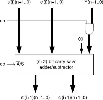
Figure 13.14 SRT-2 carry-save divider: basic cell.
The cost and computation time of the carry-save basic cell of Figure 13.14 are given by
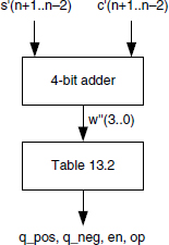
Figure 13.15 Selection of q_pos, q_neg,en,op.

Figure 13.16 SRT-2 carry-save divider: general structure.
and
Observe that (Table 13.2) the control signals op and en can be chosen equal to
so that the circuit of Figure 13.15 can be synthesized with a 4-bit adder, a 4-input 2-output look-up table, and some additional logic gates. According to Comment 6.4, in some cases a 3-bit adder can be used. So, the cost and computation time of the circuit of Figure 13.15 are approximately equal to
TABLE 13.2 Definitions

and
The cost and computation time of a carry-save SRT-2 divider, that is, Figure 13.16 with an additional (p + 1)-bit subtractor for computing q_pos − q_neg, and an additional (n + 1)-bit adder for computing r(p) = s′(p) + c′(p)), without the correction circuit, are given by
and
Thus, the computation time is a linear (not quadratic) function of p and n.
Example 13.8 (Complete VHDL source code available.) Generate a generic n-bit base-2 SRT divider with carry-save remainder. The correction cell is similar to that of Figure 13.8. The division step of Figure 13.14 is:
entity srt_cs_cell is port ( y: in std_logic_vector (N-1 downto 0); s, c: in std_logic_vector (N+1 downto 0); en, op: in std_logic; next_s, next_c: out std_logic_vector (N+1 downto 0) ); end srt_cs_cell; architecture behavioral of srt_cs_cell is signal op_y, sum: std_logic_vector (N+1 downto 0); signal cy: std_logic_vector (N+2 downto 0); begin process (en, op, y) begin if en=‘0’ then op_y<=(others=>‘0’); else if op=‘1’ then op_y<=“00”&y; else op_y<=(“11”¬(y))+1; end if; end if; end process; adder: for i in 0 to N+1 generate sum(i)<=op_y(i) xor c(i) xor s(i); cy(i+1)<=(op_y(i)and c(i))or(op_y(i)and s(i))or(s(i)and c(i)); end generate; next_s<=sum; next_c<=cy(N+1 downto 1)&‘0’; end behavioral;
The combinational circuit of Figure 13.16 is:
entity srt_cs_selection is
port (
  s, c: in std_logic_vector (3 downto 0);
  en, op: out std_logic;
  q_pos, q_neg: out std_logic
);
end srt_cs_selection;

architecture behavioral of srt_cs_selection is
signal t: std_logic_vector (3 downto 0);
begin
  t<=s+c;
  process (t)
  begin
     case t is
       when “0000”|“0001”|“0010”|“0011”=>
            q_pos<=‘1’; q_neg<=‘0’; en<=‘1’; op<=‘0’;
       when “1011”|“1100”|“1101”|“1110”=>
            q_pos<=‘0’; q_neg<=‘1’; en<=‘1’; op<=‘1’;
       when others=>--“1111” and 0100 to 1010
            q_pos<=‘0’; q_neg<=‘0’; en<=‘0’; op<=‘-’;
     end case;
  end process;
end behavioral;
The divider structure is:
entity srt_carry_save_r2 is
port (
  X: in std_logic_vector (N downto 0);
  Y: in std_logic_vector (N-1 downto 0);
  Q: out std_logic_vector (P downto 0);
  R: out std_logic_vector (N downto 0)
);
end srt_carry_save_r2;

architecture rtl of srt_carry_save_r2 is
type rems is array (0 to P) of std_logic_vector (N+2 downto 0);
signal c, s, c_o, s_o: rems;
signal q_pos, q_neg, en, op: std_logic_vector (P-1 downto 0);
signal qq: std_logic_vector (P downto 0);
signal rr: std_logic_vector (N+1 downto 0);
begin
  s(0)<=X(N)&X&‘0’; c(0)<=(others=>‘0’);
  gen_p: for i in 0 to P-1 generate
     selc: srt_cs_selection port map(s(i)(N+2 downto N-1),
               c(i)(N+2 downto N-1), en(P-i-1), op(P-i-1),
               q_pos(P-i-1), q_neg(P-i-1));
     cell: srt_cs_cell port map (Y, c(i)(N+1 downto 0),
                     s(i)(N+1 downto 0), en(P-i-1), op(P-i-1),
                  c_o(i)(N+1 downto 0), s_o(i)(N+1 downto 0));
     c(i+1)<=c_o(i)(N+1 downto 0)&‘0’;
     s(i+1)<=s_o(i)(N+1 downto 0)&‘0’;
   end generate;
   rr<=c(P)+s(P); qq<=(‘0’&q_pos) - q_neg;
   final_adjust: correction_cell port map (QQ, rr(N+1 downto 1),
                 Y, X(N), rr(N+1), Q, R);
end rtl;
Comment 13.2 The circuit of Figure 13.15 is an 8-input 2-output combinational circuit (en and op are assumed to be generated by equations (13.19)). As this circuit belongs to the critical path (p.Tcomb.circuit in (13.22)), instead of a 4-bit adder and a 4-input 2-output combinational circuit (Figure 13.15), alternative options are an 8-input 2-output optimized logic circuit, generated with Boolean minimization techniques, or an 8-input 2-output look-up table. If the most significant bits s′(n + 1) and c′(n + 1) are not used (Comment 6.4), the combinational circuit has 6 inputs and 2 outputs.
13.2.3.3 FPGA Implementation of the Carry-Save SRT-2 Divider
A FPGA implementation of the binary SRT divider cell of Figure 13.16 is shown in Figure 13.17.

Figure 13.17 SRT-2 carry-save divider: basic cell FPGA implementation.
Assuming a ripple-carry FPGA implementation for the 4-bit adder, the cost and computation time of the cell of Figure 13.17 are given by
The critical path is shaded in Figure 13.17. The cost and computation time of the binary SRT divider (Figure 13.16) are then
Observe that Tcell is a constant value so that the computation time is a linear function of p (and n if n > p).
13.2.4 SRT-4 Divider
A possible implementation of the basic cell for the SRT-4 divider is displayed in Figure 13.18. It corresponds to Algorithm 6.9. One assumes that 2.Y and 3.Y are readily available from some preliminary multiples generation and storage procedure. This cell is made up of an adder/subtractor whose inputs 0, Y, 2.Y, or 3.Y are selected through a 4-to-1 multiplexer. The q-selection circuit controls this multiplexer together with the ![]() /S input of the adder/subtractor. This circuit takes advantage of the fact that the Y coordinates of the border line staircase threshold are identified by the Boolean equation yn−1.yn−2 = 1, as shown in the P−D diagram of Figure 6.10.
/S input of the adder/subtractor. This circuit takes advantage of the fact that the Y coordinates of the border line staircase threshold are identified by the Boolean equation yn−1.yn−2 = 1, as shown in the P−D diagram of Figure 6.10.
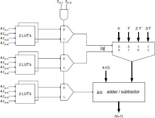
Figure 13.18 SRT-4 divider: basic cell.
The main part of the circuit may be implemented by ROMs or look-up tables: a programmable logic array has been used in the q-selection hardware of the Pentium SRT-4 division implementation. The general structure of the SRT-4 divider is shown in Figure 13.19. A correction circuit similar to that of Figure 13.8 is still needed. Moreover, an output circuit converts the final quotient Q into a nonredundant 2's complement form. If Q is given in the form of a signed 2's complement 3-bit digit vector, a circuit implementing the Booth_decode Algorithm 5.14a or 5.14b may be used. To speed up the decoding operation, on-the-fly conversion algorithms have been presented in the literature ([ERC1987], [ERC1992], [ERC1994], [MON1994]).
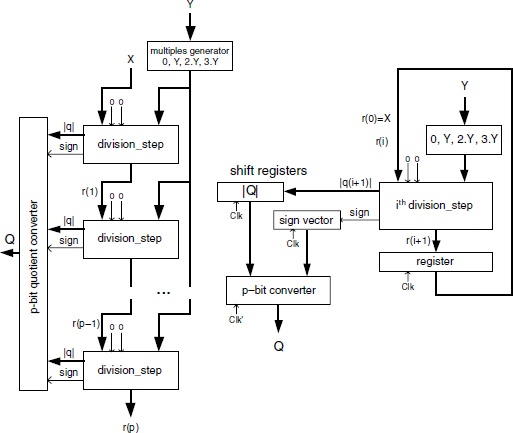
Figure 13.19 SRT-4 divider: general structure.
The cost and computation time of the SRT-4 basic cell of Figure 13.18 are given by
where the multiplexer 4−1 is assumed to be built up from 3 multiplexers 2−1. The cost and computation time of the SRT-4 divider (Figure 13.19) are then
To simplify the multiples of Y computation, an alternative of the SRT-4 algorithm has been proposed with a quotient-digit set reduced to {− 2,−1, 0, 1, 2}; so, the operations on Y are reduced to shifts only. Moreover, the range of the remainder can be restricted, typically [−2.Y/3, 2.Y/3]. The drawback of this method is the increased complexity of the quotient selection tables. Actually, more steps appear in the staircase borderlines of the P−D plot; this means more bits are needed from both the divisor Y and the shifted remainder 4.r(i) to achieve a correct selection of q. The designer is faced with an increased hardware cost for look-up tables, to be balanced against some hardware savings for Y multiples generation. Finally, depending on the available design resources and options, the basic step complexity could slow down the overall process: multiples are computed only once while p cycles are needed to produce the full quotient.
Example 13.9 (Complete VHDL source code available.) Generate a generic n-bit base-4 SRT divider with 2's complement remainder. The division step of Figure 13.18 is:
entity srt_r4_step is
  port (
    r: in STD_LOGIC_VECTOR (N+2 downto 0);
    b: in STD_LOGIC_VECTOR (N-1 downto 0);
    Q: out STD_LOGIC_VECTOR (2 downto 0);
    r_n: out STD_LOGIC_VECTOR (N+2 downto 0)
  );
end srt_r4_step;

architecture behavior of srt_r4_step is
signal mult_m: std_logic_vector(N+1 downto 0);
signal Q_digit: std_logic_vector(2 downto 0);
begin
  selection: Qsel port map (rt=>r(N+2 downto N-1),
             d_2=>b(N-2), q=>Q_digit);
  Q<=Q_digit;
  mult_m<=b*Q_digit(1 downto 0);

  add_subtract: process(mult_m,Q_digit,r)
  begin
    if Q_digit(2)=‘1’ then
      r_n<=r - mult_m;
    else r_n<=r+mult_m;
    end if;
  end process;
end behavior;
The divider structure is:
entity div_SRT_r4 is
  port (
    X: in STD_LOGIC_VECTOR (N-1 downto 0);
    Y: in STD_LOGIC_VECTOR (N-1 downto 0);
    Q: out STD_LOGIC_VECTOR (P-1 downto 0);
    R: out STD_LOGIC_VECTOR (N-1 downto 0)
  );
end div_SRT_r4;

architecture div_arch of div_SRT_r4 is

type connect is array (0 to P) of STD_LOGIC_VECTOR (N+2
downto 0); Signal wires: connect;
type Qmatrix is array (0 to P-2) of STD_LOGIC_VECTOR (2
downto 0); Signal Q_digit: Qmatrix;
Signal add,subst,the_adjust: STD_LOGIC_VECTOR (P-1 downto 0);
signal adjust: STD_LOGIC;
begin
  wires(0)<=“0”&X&“00”;
  divisor: for i in 0 to P-1 generate
  div_in: if i mod 2=0 generate
    in_step: srt_r4_step port map (r=>wires(i),
                    b=>Y, Q=>Q_digit(i), r_n=>wires(i+1));
      wires(i+2)<=wires(i+1)(N downto 0)&“00”;--X 4
    end generate;
  end generate;
  adjust<=wires(P-1)(N+2);

  correction_step: process (adjust, wires(P))
  begin
    if adjust=‘0’ then
      R<=wires(P-1)(N-1 downto 0);
    else R<=wires(P-1)(N-1 downto 0)+Y;
    end if;
  end process;
  Quotient: process(Q_digit)
  begin
    for i in 0 to P-1 loop
      if i mod 2=0 then
        if Q_digit(i)(2)=‘1’ then--positive
          add(P-i-1 downto P-i-2)<=Q_digit(i)(1 downto 0);
          subst(P-i-1 downto P-i-2)<=“00”;
        else- -negative
          add(P-i-1 downto P-i-2)<=“00”;
          subst(P-i-1 downto P-i-2)<=Q_digit(i)(1 downto 0);
        end if;
      end if;
    end loop;
  end process;
  the_adjust(0)<=adjust; the_adjust(P-1 downto 1)<=(others=>
  ‘0’);
  Q<=add-subst-the_adjust;
end div_arch;
13.2.5 Convergence Dividers
Two convergence dividers are presented in this section: the Newton–Raphson divider and the Goldschmidt divider. Basically, the complexity of the involved algorithms is proved to be better than the one of recurrence dividers (Chapter 6). Nevertheless, the overall performances will depend on the performance of the multiplication involved in each step. So the use of these dividers should be considered as part of a more complex system such as, for example, an arithmetic and logic unit.
13.2.5.1 Newton–Raphson Divider
The basic cell of the Newton–Raphson divider computes (formula (6.62))
![]()
that is, two dependent multiplications and a subtraction. As quoted in Chapter 6, a B's complement operation may replace the subtraction. The basic cell and the general structure of an n-digit, precision p Newton–Raphson divider are shown in Figure 13.20, where it is assumed that p ≥ n. The basic cell can iteratively use the same multiplier; this would require two clock cycles per step. Assuming d ≥ 0.1, t + 2 digit LUT inputs ensure a t-bit precision (error < B−t) in the first estimation. Then, the minimum precision p will be achieved after k = [log2 p/t] steps. The final multiplication of the dividend by x(k), the inverse of the divisor, is implicit in the general structure of Figure 13.20.
The cost and computation time of the Newton–Raphson basic cell, using a single multiplier within two clock cycles, are given by

Figure 13.20 Newton–Raphson divider.
The cost and computation time of the Newton–Raphson divider as shown in Figure 13.20 are then
where (i) a k-step sequential implementation, (ii) a 2-cycle division step (one multiplier), and (iii) a shared (with basic cell) multiplier for the final multiplication have been assumed.
Example 13.10 (Complete VHDL source code available.) Generate a generic n-bit base-2 Newton–Raphson inverter. The division step of Figure 13.20 is:
entity newton_raphson_step is
generic(L: integer);
  port (
    r: in std_logic_vector (L downto 0);
    d: in std_logic_vector (N-1 downto 0);
    r_n: out std_logic_vector (2*L downto 0)
);
end newton_raphson_step;

architecture behavioral of newton_raphson_step is
signal r_x_d, r_x_d_neg: std_logic_vector (L+N downto 0);
signal r_n_long: std_logic_vector (2*L+N+1 downto 0);
begin
  r_x_d<=r*d;
  r_x_d_neg<=not(r_x_d)+1;
  r_n_long<=r*r_x_d_neg;
  r_n<=r_n_long(2*L+N downto N);
end behavioral;
The inverter structure is:
entity newton_raphson is
  port (
    X: in std_logic_vector (N-1 downto 0);
    Q: out std_logic_vector (P downto 0)
  );
end newton_raphson;

architecture behavioral of newton_raphson is
constant LOG_P: natural:=log_base_2(P);
constant LOG_F: natural:=log_base_2(F);
type rmd is array (0 to LOG_P-1) of std_logic_vector (P
downto 0);
signal r: rmd;
signal lut_val: std_logic_vector (F downto 0);

begin
  lut: LUT_Newton_Raphson port map (x=>X, l=>lut_val);
  r(LOG_F-1)(P downto P-F)<=lut_val;
  gen_p: for i in LOG_F to LOG_P-1 generate
    cell: newton_raphson_step generic map(2**i)
      port map (r=>r(i-1)(P downto P-2**i),
        d=>X, r_n=>r(i)(P downto P-2**(i+1)));
    end generate;
  Q<=r(LOG_P-1)(P downto 0);
end behavioral;
13.2.5.2 Goldschmidt Divider
The basic cell of the Goldschmidt divider computes (formulas (6.72))
![]()
![]()
D(0) and d(0) are initially set to the dividend and the divisor, respectively. The basic cell and the general structure of the Goldschmidt divider are presented in Figure 13.21. As stated in Chapter 6, a look-up table procedure can refine those initial values in order to speed up the convergence process. This alternative is not represented in the basic cell scheme. An important feature of the Goldschmidt basic cell is the independence of the multipliers; so the multiplications may be either performed in parallel or pipelined into a unique multiplier. The pipeline alternative is quite attractive for its lower cost in most design environments. A typical case is that of Xilinx FPGA, where flip-flops are readily available in every slice.
The cost and computation time of the Goldschmidt basic cell, using a single pipelined multiplier, are given by
The cost and computation time of the Goldschmidt divider as shown in Figure 13.21 are then
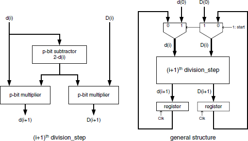
Figure 13.21 Goldschmidt divider: basic cell and general structure.
Example 13.11 (Complete VHDL source code available.) Generate a generic n-bit base-2 Goldschmidt divider. The division step of Figure 13.21 is:
entity goldschmidt_step is
generic(L: integer:=4);
port (
    r: in std_logic_vector (P-1 downto 0);
    d: in std_logic_vector (P-1 downto 0);
    r_n: out std_logic_vector (P-1 downto 0);
    d_n: out std_logic_vector (P-1 downto 0)
);
end goldschmidt_step;

architecture behavioral of goldschmidt_step is
signal d_neg: std_logic_vector (L downto 0);
signal d_neg_long: std_logic_vector (P downto 0);
signal r_n_long, d_n_long: std_logic_vector (P+L downto 0);
begin
  d_neg_long<=not(‘0’&d);
  d_neg<=d_neg_long(P downto P-L);
  r_n_long<=r*d_neg;
  r_n<=r_n_long(P+L-1 downto L);
  d_n_long<=d*d_neg;
  d_n<=d_n_long(P+L-1 downto L);
end behavioral;
The divider structure is:
entity goldschmidt is
port (
  X: in std_logic_vector (N-1 downto 0);
  Y: in std_logic_vector (N-1 downto 0);
  Q: out std_logic_vector (P-1 downto 0)
);
end goldschmidt;

architecture behavioral of goldschmidt is
type re is array (0 to LOGP+1) of std_logic_vector (P-1
downto 0);
signal r, d: re;
begin
  r(0)(P-1 downto P-N)<=X; r(0)(P-N-1 downto 0)<=
  (others=>‘0’);
  d(0)(P-1 downto P-N)<=Y; d(0)(P-N-1 downto 0)<=
  (others=>‘0’);
  gen_p: for i in 0 to LOG_P-1 generate
    cell: goldschmidt_step generic map(2**(i+1))
          port map (r(i),d(i),r(i+1), d(i+1));
  end generate;
  celln: goldschmidt_step generic map(P)
      port map (r(LOG_P), d(LOG_P), r(LOG_P+1), d(LOG_P+1));
  Q<=r(LOG_P+1)(P-1 downto 0);
end behavioral;
13.2.5.3 Comparative Data Between Newton–Raphson (NR) and Goldschmidt (G) Implementations
From the algorithmic point of view the main facts are (Chapter 6):
- G algorithm converges toward the quotient while NR algorithm doesn't, it converges toward the inverse of the divisor and then multiplies by the dividend.
- G is not self-correcting, errors propagate; NR compensates errors.
- Multiplications are independent in G, not in NR.
- Neither algorithm can provide the exact remainder.
- Both algorithms essentially consist of two multiplications and one subtraction (or base complement).
- For both algorithms, convergence rate is quadratic.
At the implementation level the main consequences of the preceding are the following:
- An additional multiplication is needed by NR; this consumes time, increases cost or both but this can be negligible in the overall performance.
- The rounding operations are more critical for G.
- Multiplications can be made in parallel or pipelined in G; this can save time at a reasonable cost.
As a conclusion on convergence methods, one can state that those algorithms compete with each other. The technology at hand, the performance criteria, and a number of constraints are finally the key for a reasonable algorithm selection. Experimental designers feel that as well as sound theoretical options, smart designing techniques may significantly improve the overall quality of a particular algorithm implementation. Newton–Raphson dividers have been used, among others, by Intel and IBM ([INT1989], [MAR1990]); Goldschmidt dividers appear in some IBM and Advanced Micro Device processors ([AND1967], [OBE1999]).