10.1 RESOURCES
In order to synthesize a digital circuit the designer has to develop—or states the necessity to develop—computation, memory, and connection resources:
- The computation resources are deduced from the operations included in the algorithm; they are characterized by their functions, their computation times, and their costs.
- The memory resources are registers, banks of registers, random access or read-only memories, stacks, and queues, characterized by their minimum setup and hold times, maximum propagation time, and read and write cycles, among other features, as well as by their costs.
- The connection resources are multiplexers and tristate buffers used for controlling the transfer of data between computation resources and registers; they are characterized by their propagation times and costs.
Consider two examples
Example 10.1 (Combinational circuit; complete VHDL source code available.) Synthesize an n-bit adder based on Algorithm 4.2 with B = 2. The corresponding computation resources are:
- the carry-propagate function p defined by p(a, b) = 1 iff a + b = 1, that is, a 2-input XOR gate;
- the carry-generate function g defined by g(a, b) = 1 if a + b > 1, any value if a + b = 1,0 if a + b < 1 (Comment 4.1(2)) so that g could be chosen equal to a, b or a · b; let it be b;
- the 3-operand mod 2 sum: mod_sum(a, b, c) = (a + b + c) mod 2, that is, a 3-input XOR gate equivalent to two 2-input ones.
The only connection resource type is a 2-to-1 multiplexer able to transfer either q(i) or g(i) to q(i + 1).
If there is no restriction as regards the number of resources, a combinational (memoryless) circuit can be synthesized. An example is shown in Figure 10.1 (its corresponding FPGA implementation is described in Chapter 11).
Its costs and delays are equal to
where CXOR2 and CMUX2−1 are, respectively, the costs of a 2-input XOR gate and of a 2-to-1 one-bit multiplexer, while TXOR2 and Tmux2−1 are the corresponding propagation times.
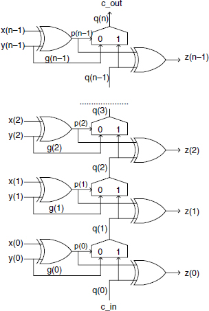
Figure 10.1 Combinational n-bit adder.
The corresponding VHDL model is the following one:
entity example10_1 is
port (
  x, y: in std_logic_vector(n-1 downto 0);
  c_in: in std_logic;
  z: out std_logic_vector(n-1 downto 0);
  c_out: out std_logic
);
end example10_1;
architecture circuit of example10_1 is
  signal p, g: std_logic_vector(n-1 downto 0);
  signal q: std_logic_vector(n downto 0);
begin
  q(0)<=_in;
  iterative_step: for i in 0 to n-1 generate
    p(i)<=x(i) xor y(i);
    g(i)<=y(i);
    with p(i) select q(i+1)<=q(i) when ‘1’, g(i) when others;
    z(i)<=p(i) xor q(i);
  end generate;
  c_out<=q(n);
end circuit;
Example 10.2 (Complete VHDL source code available.) As a second example—this one including memory resources—an m-operand n-bit adder is synthesized. It is based on Algorithm 4.11 with B = 2. The only computation resource is an n-bit adder. A memory resource, namely, an n-bit register, is necessary in order to store the value of the variable accumulator. Two connection resources must be used: the first one, an m-to-1 n-bit multiplexer, selects the second operand x(j) as a function of j; the other one, a 2-to-1 n-bit multiplexer loads either 0 or the adder output within the register.
The corresponding circuit is made up of a data path (Figure 10.2) and a control unit generating the signals op_select, clear, and load. In order to allow the connection of the circuit to some main processor, the control unit is also in charge of a start/done communication protocol.
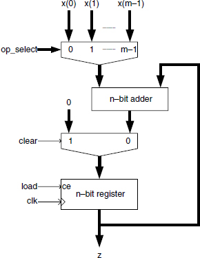
Figure 10.2 Data path of an m-operand adder.
The cost C and the delay T of the data path are equal to
where CFF is the cost of a 1-bit register (e.g, a D flip-flop) and TFF is the propagation time—it is assumed that the m-to-1 multiplexer is implemented by a tree-like log2 m level circuit made up of 2-to-1 multiplexers.
The datapath VHDL model is the following one:
entity data_path is
port(
  operands: in operand_matrix;
  clk, clear, load: in std_logic;
  op_select: in std_logic_vector(logm-1 downto 0);
  z: out std_logic_vector(n-1 downto 0)
  );
end data_path;

architecture circuit of data_path is
  signal op_1, op_2, adder_out, reg_in, reg_out:
  std_logic_vector(n-1 downto 0);
begin
  op_1 <=operands(conv_integer(op_select));
  op_2<=reg_out;
  adder_out<=op_1+op_2;
  with clear select reg_in<=adder_out when ‘0’,
  conv_std_logic_vector(0, n) when others;
  process(clk)
  begin
    if clk'event and clk=‘1’ then
    if load=‘1’ then reg_out<=reg_in; end if;
    end if;
  end process;
  z<=reg_out;
end circuit;
The control unit is a finite state machine whose VHDL model is the following one:
entity control_unit is
port(
  clk, start, reset: in std_logic;
  done, clear, load: out std_logic;
  op_select: out std_logic_vector(logm-1 downto 0)
  );
end control_unit;

architecture fsm of control_unit is
  subtype state is integer range-3 to m;
  signal current_state: state;
begin
  process(clk, reset)
  begin
    case current_state is
      when -3=>clear<=‘1’; load<=‘0’;
      op_select<=conv_std_logic_vector(0, logm); done<=‘1’;
      when -2=>clear<=‘1’; load<=‘0’;
      op_select<=conv_std_logic_vector(0, logm); done<=‘1’;
      when -1=>clear<=‘1’; load<=‘1’;
      op_select<=conv_std_logic_vector(0, logm); done<=‘1’;
      when 0 to m-1=>clear<=‘0’; load<=‘1’;
      op_select<=conv_std_logic_vector(current_state, logm);
      done<=‘0’;
      when m=>clear<=‘0’; load<=‘0’;
      op_select<=conv_std_logic_vector(0, logm); done<=‘1’;
    end case;
    if reset=‘1’ then current_state<=-3;
    elsif clk'event and clk=‘1’ then
      case current_state is
        when -3=>if start=‘0’ then
        current_state<=current_state+1; end if;
        when -2=>if start=‘1’ then
        current_state<=current_state+1; end if;
        when -1=>current_state<=current_state+1;
        when 0 to m-1=>current_state<=current_state+1;
        when m=>current_state<=-3;
      end case;
    end if;
  end process;
end fsm;
If a minimum number of state-encoding variables are used, and if the combinational cost is small compared with the state-register one, the cost of the control unit is roughly equal to log2(m + 4).CFF.
The total cost of the m-operand adder is equal to
and its computation time to