
9.1 DESIGN METHODS FOR ELECTRONIC SYSTEMS
With the passing of time, integrated circuit (IC) technology has provided a variety of implementation formats for system designers. The implementation format defines the technology to be used, how the switching elements are organized and how the system functionality will be materialized. The implementation format also affects the way systems are designed and sets the limits of the system complexity. Today the majority of IC systems are based on complementary metal-oxide semiconductor (CMOS) technology. In modern digital systems, CMOS switching elements are prominent in implementing basic Boolean functions such as AND, OR, and NOT. With respect to the organization of switching elements, regularity and granularity of elements are essential parameters. The regularity has a strong impact on the design effort, because the reusability of a fairly regular design can be very simple. The problem raised by the regularity is that the structure may limit the usability and the performances of the resource. The granularity expresses the level of functionality encapsulated into one design object. Examples of fine-grain, medium-grain, and coarse-grain are logic gates, arithmetic and logic units (ALUs), and intellectual property components (processor, network interfaces, etc.), respectively. The granularity affects the number of required design objects and, thereby, the required design or integration effort.
Depending on how often the structure of the system can be changed, the three main approaches for implementing its functionality are dedicated systems, reconfigurable systems, and programmable systems. In a dedicated system, the structure is fixed at the design time, as in application-specific integrated circuits (ASICs). In programmable systems, the data path of the processor core, for example, is configured by every instruction fetched from memory during the decode-phase. The traditional microprocessor-based computer is the classical example. In reconfigurable systems, the structure of the system can be altered by changing the configuration data, as in field programmable gate arrays (FPGAs).
9.1.1 Basic Blocks of Integrated Systems
The basic building blocks for digital ICs are input, output, data path, memory, and control, as in a common computer (Figure 9.1). Additionally, a communication network is necessary to interconnect the blocks. The implementation format of each basic block can, at least theoretically, be any combination of the previous classes.
The data path consists of regular elements, as in reconfigurable arrays, or dedicated pipelined blocks, as in superscalar processors. The granularity of data path elements can vary from single gates to processor arrays in multiprocessor architectures. A typical data path consists of an interconnection of basic logic (AND, OR, etc.), arithmetic operators (adders, multipliers, shifters, complement), and registers to store the intermediate results.
The memory can be characterized by size, number of ports, latency, and bandwidth. Latency is the access delay of a randomly chosen data element and bandwidth is the data rate. Memory components are typically two-dimensional regular structures, and latency is inversely proportional to the size of memory. The bandwidth depends on the memory buses, the internal organization of the memory, and the access logic. The memory is typically organized hierarchically. The faster and more expensive memories are near the data path; slower, bigger and cheaper memories are used to store less-frequently accessed data.

Figure 9.1 Components of a generic digital processor; arrows represent interconnection network.
The main two memory classes are volatile memories, such as, for example, static random-access memory (SRAM) or dynamic random-access memory (DRAM), and nonvolatile memories, such as read-only memory, (ROM), and FLASH memory. SRAM is a fast memory, but typical implementations need six transistors per bit. DRAM is a dense memory, with only one transistor per bit, but the latency (i.e., access delay) is high. The FLASH memory also suffers from high latencies. The DRAM and FLASH memories are internally asynchronous and have different latencies for random and sequential accesses. For DRAM, in particular, a variety of solutions have been proposed for speeding up the overall performances, among them fast page mode accesses, synchronous interfaces, and intelligent control interfaces.
The communication network is another important component of an electronic system. Communication channels can be divided into dedicated channels (signals) and shared channels (buses and networks). The buses connect subsystems, and networks connect full systems according to the classical definition. The dedicated channels may be static point-to-point connections or dynamic switched connections. The buses can be further divided into data path memory and input/output (I/O) buses, parallel and serial buses, or synchronous and asynchronous buses, according to their purpose or physical implementation.
The control module determines what actions are carried out by the data path at any time, when and how memory, I/O modules, and data path are communicated or related. A controller is implemented as a finite state machine (FSM). The logic of a FSM can be implemented in different ways, with basic logic gates (AND, OR, NOT), using arrays of programmable logic devices (PLDs), or programming a memory (microprogramming). The way to implement FSM registers depends on the selected technology.
The input/output modules are used to connect the system to the outside world. These modules are most often slower than the other system parts. The throughput necessary in the I/O defines the communication network and the whole system organization.
9.1.2 Recurring Topics in Electronic Design
In the electronics industry, competition of one form or another leads to smaller, faster, cheaper, and better products and related manufacturing techniques. Gordon Moore's ([MOO1965]) insight, that the density of chips would double every 18 months, has proved incredibly accurate, and there is no end in sight. Nowadays, electronics industry leaders apply this principle to forecast three generations ahead. This competition and rapid growth create outstanding electronic design challenges.
9.1.2.1 Design Challenge: Optimizing Design Metrics
The obvious design goal is to construct and implement within the desired functionality, but the key design challenge comes from the need for simultaneous optimizations with respect to numerous design metrics. The most common metrics are cost, size (physical space required by the system), performance, power consumption, flexibility, time-to-prototype (time needed to build a first working version of the system), time-to-market, maintainability, correctness, and safety. Competition generally exists between design metrics criteria; improving one may worsen others (Figure 9.2). Expertise with both software and hardware is needed to optimize design metrics. The designer must feel comfortable with various technologies in order to choose the best for a given application within given constraints. Some key concepts in electronic design are presented in what follows.
9.1.2.2 Cost in Integrated Circuits
When costs in electronic design are considered, one needs to worry about two main kinds of costs:
- Cost of development, sometimes called nonrecurring engineering (NRE) cost.
- Cost of manufacturing each copy of the system, called unit cost (UC).
The total cost, TC, is then readily calculated as
![]()
where Q stands for the quantity of units. The final cost, FC, per product (per-product cost) is then equal to
![]()
Trade-off strategies have to be implemented in relation to NRE and manufacturing costs. For example, according to Sperling ([SPE2003]), the NRE cost for the design of an ASIC, within the 100 nm, or less technology, can run around several million U.S. dollars; thus the manufactured quantities need to be important, that is, great enough to offset the impact of the NRE cost on the final cost. Figure 9.3 shows the evolution of the total costs with respect to manufactured quantities, marking low and high initial NRE costs (lines A and B, respectively).

Figure 9.2 Design metrics competition.

Figure 9.3 Cost evaluation as a function of manufactured quantities.
9.1.2.3 Moore's Law
In 1965, just four years after the first planar integrated circuit was discovered, Gordon Moore, cofounder of Intel™, made his famous observation about chip density growth. This is since referred to as ‘Moore's law’. In his original paper ([MOO1965]), Moore observed an exponential growth in the number of transistors per integrated circuit and predicted that this trend would continue. In the following years, the pace slowed down a little bit, but data density has doubled approximately every 18 months, and this is the current definition of Moore's law. Figure 9.4 shows transistor density increment for Intel™ processors. In today's electronic world, these rules are also valid for memory capacities and computer systems performance.
9.1.2.4 Time-to-Market
The time-to-market is the time required to develop a product up to the point it can be sold to customers. In today's electronics, it is one of the most important metrics. In most design projects, the average time- to-market constraint is about 6 to12 months; extra delays could lead to unaffordable costs. An important related concept is the market window, that is, the period during which the product would have the highest sales. Figure 9.5 shows a typical market window and a simplified revenue model. In this model, the product life is equal to 2.P and the revenue's peak occurs at the half-life P; D represents the time delay.

Figure 9.4 Moore's law for transistor capacity in Intel™ microprocessors.
This simplified model assumes that both market rise and market fall behaviors are linear; the market rise slope is the same for both on-time and delayed entries while the market fall assumes, for both cases, the same date for market zero. Time-revenue diagrams of market entries define triangles representing market penetration; triangle areas represent revenues. The percentage of revenue losses, materialized by the difference between the on-time and the delayed zone areas are then readily computed as 1 − (2.P − D)(P − D)/2.P2, where 2.P is the full lifetime of the product and D the delay. For instance, a delay of 5 weeks for a product with a lifetime 2.P of one year (52 weeks) generates a loss of roughly 27%, but with a 3-month delay (13 weeks) the loss rises to 62.5%! This shows that delays are extremely expensive and therefore one of the most important driving forces in the IC industry; this motivates efforts toward new methodologies, design methods, and EDA tools.
9.1.2.5 Performance Metric
The performance design metric is widely used to measure the “system quality,” but it is also widely abused. The clock frequency and quantity of instructions per second are common criteria, but they are not always good enough as performance measures. For instance, in a digital camera, the user cares more about how fast it starts up or processes images, than about the internal clock frequency or instructions processing speed of the internal processor. More accurate and useful performance metrics are latency and throughput. Latency (response time) measures the time between the start and end of a task: in the camera example, it could be the time to process an image, for example, 0.25 second (camera A) or 0.20 second (camera B). The throughput is defined as the quantity of tasks performed per second, for example, for the above cameras, 4 and 5 images per second, respectively. Observe that the throughput can be greater than the inverse of the latency thanks to possible concurrency or pipelining, for example, camera A could process 8 images per second, instead of 4, by capturing a new image while the previous image is being stored. Another useful metric is speedup, that is, comparing two performances: in the previous example, the throughput speedup of the pipelined processor of camera A over the one of camera B, is computed as A's performance/B's performance, that is, 8/5 = 1.6.
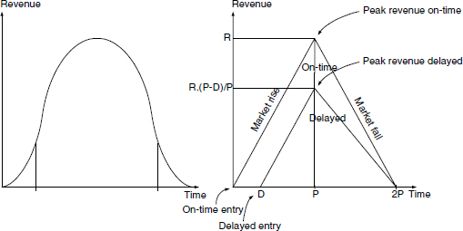
Figure 9.5 Typical distribution of a market window—simplified revenue model.
9.1.2.6 The Power Dimension
With the booming market of portable electronic devices, power consumption has turned out to be an important parameter in the design of integrated circuits. It allows avoiding expensive packaging: the chip lifetime is increased, cooling is simplified, and battery-powered systems take advantage of increased autonomy and reduced weight.
There are two modes of power dissipation in integrated circuits: power generated during static operation or dynamic operation. Static power dissipation comes from currents flowing while no switching occurs. These include currents due to pn-junctions, static currents due to device biasing, and leakage currents. Dynamic power dissipation is a result of switching activities, whenever currents cause capacitances to be charged or discharged while performing logic operations. In CMOS devices the dissipated dynamic power P is proportional to the loading of capacitances C, the switching frequency F, and the square of supply voltage V:
![]()
While power was becoming important in CMOS devices, designers have developed a number of tools and techniques to reduce the required power consumption. In CMOS devices, most of the power is used for voltage value switching on a wire; therefore most of the power reduction techniques try hard to ensure that a signal is not changed unless it really should be, then preventing other wasteful power sources. The power saving techniques range from simply turning off the processor/system when inactive—a technique used in almost all portable systems—to a careful power control of individual chip components. Observe, moreover, that power is very strongly related to the chip performance. A circuit can almost always be designed to require less energy for a task, if it is given more time to complete it. This has recently led to a set of techniques for dynamical control of the performances, to be kept as small as necessary to minimize the power used.