
Oxide nanowires for nonvolatile memory applications
K. Nagashima; T. Yanagida Osaka University, Osaka, Japan
Abstract
Nanowires provide unique tools for scaling down in semiconductor electronics and the fundamental understanding of nanoscale physical phenomena, which are not accessible in conventional lithography. Resistive random access memory (ReRAM) is an emergent concept in nonvolatile memory to overcome the limitations of flash memory technology; however, its potential scalability and the fundamental nanoscale mechanism have been controversial. This chapter reviews oxide nanowire-based ReRAM. The oxide nanowire allows for ultrasmall device architecture such as a segmented memory cell in a single nanowire and a cross-bar memory cell at a nanowire junction. Furthermore, the nanoscale physical mechanisms of ReRAM are directly extracted by the confined space of the oxide nanowire. First, the memory performance of oxide nanowire ReRAM, including their cell sizes, is discussed, and later, the detailed mechanism, the challenging issues, and the application field of oxide nanowire ReRAM are discussed.
16.1 Introduction
Nonvolatile memory was rapidly developed in the early twenty-first century with the scaling of flash memory technology. Flash memory is based on the metal-oxide-semiconductor field effect transistor combined with floating gate structure and is expected to face scaling limitations in the 2010s (Meijer, 2008). The alternative idea is to keep increasing the density and performance of nonvolatile memory. Two clear directions are proposed to solve the scaling issue. One is to employ the three-dimensional (3-D) flash memory architecture, of which the conducting channel is aligned vertically (Park et al., 2012). In the 3-D memory device structure, the density of memory increases with an increased number of laminations. Another idea is to explore the novel nonvolatile memory concept, which differs from flash memory (Meijer, 2008). The novel concept relies on the simple device structure and memory performance beyond flash memory technology. The latter idea is a fascinating solution for the sustainable scaling of nonvolatile memory because it allows both the simplification of the component device cell and the 3-D architecture for device integration in principle.
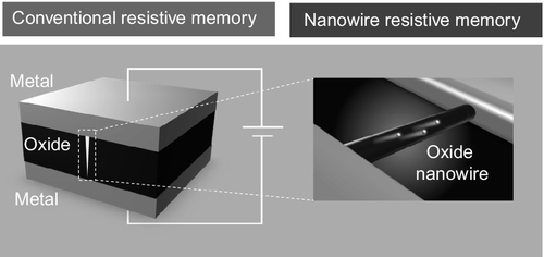
Among the various novel nonvolatile memory concepts, including phase change memory and ferroelectric memory, a nonvolatile memory using a resistance switching in metal/insulator/metal structure, the so-called resistive random access memory (ReRAM) or memristor, is promising as an alternative to flash memory due to its structural simplicity and the memory performance, including high switching speed and endurance (Waser et al., 2009; Lee et al., 2011; Torrezan et al., 2011; Yang et al., 2013). ReRAM can be integrated using the crossbar array rule (Yang et al., 2008). In crossbar array, the size of a single device can be designed by only 4F2, where F is the designable minimum size scale defined by the lithography technique. Historically, Hickmott first discovered the resistance-switching phenomenon in aluminium oxides in 1962 (Hickmott, 1962). Since then, enormous investigations have been continuously devoted to increasing the memory performance and clarifying the fundamental physical mechanism of resistive switching using oxides (Waser et al., 2009; Lee et al., 2009, 2010, 2011; Torrezan et al., 2011; Yang et al., 2008, 2010, 2013; Seo et al., 2004; Szot et al., 2006; Strachan et al., 2011; Yanagida et al., 2013; Nagashima et al., 2013). The most interesting feature of ReRAM is its transport property. The electrical transport of ReRAM is associated with the extremely small conducting filaments in the insulative matrix of oxide (Waser et al., 2009). The cross-sectional size of the conducting filaments is experimentally and theoretically assumed to be 1–10 nm (Kwon et al., 2010; Yang et al., 2012; Ielmini et al., 2010). This promises to scale the ReRAM down to around 10 nm because the transport properties must not be interfered with until the device size becomes comparable to the size of filament. However, the potential scalability and the nanoscale mechanisms of ReRAM have been controversial due to the lack of a technique to directly evaluate such issues. Oxide nanowire grown by the bottom-up method gives an extremely small cross-sectional area, which is not achievable by conventional lithographic techniques. Therefore, it is rational to use oxide nanowire not only for investigating the scalability of ReRAM but also for clarifying the underlying nanoscale physical mechanism of the conducting filaments because the oxide nanowire can in principle capture the conducting filaments into nanowire (Figure 16.1). This chapter reviews the ultrasmall resistive memory and the physical mechanism of resistive memory using the unique structure of oxide nanowire. In Section 16.2, the characteristics of oxide nanowire-based resistive memory are described together with the fabrication technique of oxide nanowires. In Section 16.3, the fundamental physical mechanisms of resistive switching, which had never been accessible by conventional ReRAM device structure, are described. The challenging issues and the possible application fields of oxide nanowire memory are discussed in Section 16.4.
16.2 Oxide nanowire for ultrasmall memory applications
First, resistive memory should be described. In general, the resistive switching in a metal/oxide/metal capacitor structure is associated with the electrical breakdown phenomenon (Waser et al., 2009; Yang et al., 2013). When the relatively high electric field is applied between two metal electrodes, electrical breakdown occurs in oxide, accompanying the drastic reduction of the resistance of the capacitor (Waser et al., 2009; Yang et al., 2013). In the meantime, the nanoscale conducting filaments locally generate in the insulative oxide matrix and govern the transport properties of the capacitor (Waser et al., 2009; Kwon et al., 2010; Yang et al., 2012). Such nanoscale conducting filaments are stably maintained even if the electric field is removed; thereby the resistive switching shows a nonvolatility. When the conducting filaments are diminished via the external stimuli (e.g., the electric field with inverse polarity or thermal energy), the resistance of the capacitor changes to insulative state. Because the electrical transport of the capacitor relies on the conducting filaments, manipulating the filaments is crucial to determine the performance of resistive memory (Yanagida et al., 2013). Although the filament model is taken in this chapter, it should be noted that the filament model is also applicable to the homogeneous resistive switching model, which is reported by several groups (Sawa, 2008; Yasuhara et al., 2010), if the filaments are uniformly distributed within the oxide.
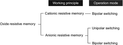
The resistive memory can be classified into several groups based on its mechanism and operation mode, as shown in Figure 16.2. First, resistive memory is generally classified into two groups based on the working principle. For a ‘cationic’ resistive memory, the nanoscale conducting filaments are created by the migration of metal electrode. In this memory, Ag or Cu is utilized for a source of metallic filament, and the oxide layer works as a solid electrolyte (Waser et al., 2009; Yang et al., 2012). For an ‘anionic’ resistive memory, the resistive switching is caused by the resistance change in oxide (Yang et al., 2008). The resistive memory can be further classified via the operation mode (i.e., bipolar resistive switching and unipolar resistive switching). Figure 16.3 shows the typical current–voltage (I–V) characteristics of both bipolar and unipolar resistive switching. For both resistive switching, the resistance changes from insulative OFF state to conductive ON state (so-called SET process) occur through the electrical breakdown process when the high electric field above the threshold value is applied. The compliance current is always employed to prevent a destructive permanent breakdown. In bipolar resistive switching, the inverse resistive switching from conductive ON state to insulative OFF state (so-called RESET process) is available under the electric field with opposite polarity, whereas in the unipolar resistive switching the resistance switching always occurs at the same electric field polarity. In anionic resistive memory, both unipolar and bipolar resistive switchings have been observed; however, in cationic resistive memory bipolar resistive switching has been mainly observed (Waser et al., 2009).

This section reviews the oxide nanowire-based resistive memory, covering both the cationic and the anionic switching principles. The memory performance of each resistive memory such as the cross-sectional device size, the working voltage/current and the endurance is discussed. The potential scalability of ReRAM has been demonstrated via the several nanowire structures including (i) simple oxide nanowire structure, (ii) segmented nanowire structure and (iii) nanowire crossbar junction structure.
16.2.1 Resistive switching in oxide nanowire
Resistive switching in oxide nanowire was first reported by Kim et al. (2008). They employed NiO nanowire for anionic restive switching. The NiO nanowires were fabricated by the anodized aluminium oxide (AAO) template method as shown in Figure 16.4. The AAO template was fabricated via the two-step anodizing process. First, high-purity aluminium was anodized under a constant voltage in oxalic acid solution. Then the aluminium oxide layer was chemically removed. The anodizing process was repeated, and the AAO template with hexagonally aligned nanopores was obtained. Ni nanowires were then obtained by the electrochemical deposition of Ni into the nanopores of AAO template. Finally polycrystalline NiO nanowires with 70 nm diameter were obtained by thermal oxidization of Ni nanowires for 7 h at 450 °C. The grain size was larger than or comparable to the diameter of NiO nanowires. The thermal treatment was carried out by checking the resistance of the nanowire, and the nanowire resistance was controlled to be 100 MΩ.

The electrical transport property was performed using an individual NiO nanowire device. Prior to the construction of a NiO nanowire device, the AAO template was completely dissolved. The device was fabricated onto a silicon substrate covered by a thermally oxidized SiO2 layer. The Au/Ti electrodes were patterned onto a single NiO nanowire by conventional lithographic technique. The gap size between electrodes was 1 μm. First, a forming process, which is an initiation process for the resistive switching with a relatively high voltage was performed at 2.5 V. After the forming process, the resistance of the device changed into a conductive state. Subsequently, the device showed the continuous unipolar resistive switching under the positive electric field as seen in Figure 16.5. The SET voltage, the RESET voltage and the RESET current of the NiO nanowire device were 1.2 V, 0.52 V and 2.3 × 10− 4 A, respectively. Interestingly, a weak dependence of RESET current on the device size (RESET current ∝ A0.38) was found, indicating that the transport property of NiO nanowire device was dominated by the localized conducting filaments. It should be noted here that the electric field intensity for forming in a 1 μm long NiO nanowire device (25 kV/cm) was almost two orders of magnitude lower than that of 20–300 nm thick NiO thin film device (> 0.1 MV/cm) (You et al., 2006). Because the forming voltage of the thin film device strongly depends on its thickness (Yanagida et al., 2013), the forming voltage over 100 V should be expected for a 1 μm long NiO nanowire device. The small forming voltage might be understood by the percolation nature of conducting filaments through the incompletely oxidized NiO in nanowire or at grain boundary rather than the localized resistive switching at the nanowire/electrode interface. This was experimentally confirmed by the length dependence on the forming voltage. The clear increase of forming voltage (20 V) was observed when a 25 μm long NiO nanowire was employed.

The large voltage for resistive switching was also found in the report by Oka et al. (2009a). Oka et al. first demonstrated the resistive switching in a single crystalline MgO–NiO core–shell nanowire. To fabricate the MgO–NiO core–shell nanowires, the in situ heterointerface fabrication technique was employed (Nagashima et al., 2008a; Marcu et al., 2008; Oka et al., 2009b). First single crystalline MgO nanowires were grown by a vapour–liquid–solid (VLS) mechanism through the pulsed laser deposition (PLD) technique (Nagashima et al., 2007a,b, 2008b; Marcu et al., 2007; Yanagida et al., 2007, 2008a,b). For the VLS growth, Au metal catalyst was utilized to conduct the MgO nanowire growth. The diameter of MgO nanowires can be definitely controlled by the size of metal catalyst. After the MgO nanowire growth, NiO was deposited onto the nanowire at 300 °C and 0.1 Pa of oxygen partial pressure. Because MgO (a = 4.21 Å) and NiO (a = 4.17 Å) are both cubic structure with a lattice mismatch of 0.7%, a single crystalline NiO shell layer was epitaxially grown onto MgO nanowires. The fabricated core–shell oxide nanowires were composed of 10 nm diameter of MgO nanowire and 10 nm thickness of NiO shell layer, resulting in 10− 3 μm2 of cross-sectional that are of NiO for resistive switching.
The electrical transport of the individual MgO–NiO nanowires was carried out with Pt/MgO–NiO nanowire/Pt-coated cantilever using conductive atomic force microscopy (C-AFM) (Oka et al., 2009a). The nanowires were first developed onto 300 nm SiO2 coated silicon substrate, then Pt electrode was deposited by using a metal mask to create the electrical contact with nanowire. After checking the exact position of nanowire on the substrate by tapping mode AFM, the electrical measurement using C-AFM was carried out at a position around 1 μm away from the Pt electrode. Before the resistive switching, the resistance of NiO was around 1011 Ω, which were three orders of magnitude higher than that of polycrystalline NiO nanowire reported by Kim et al. (2008). This is because the NiO shell layer was fully oxidized, and the defect concentration of single crystalline NiO shell layer might be less than that of polycrystalline NiO nanowire in Kim et al. (2008). Clearly, the MgO–NiO core–shell nanowire exhibited the bipolar resistive switching behaviours with the current range of 10− 8 A (Figure 16.6). The SET and RESET voltage were, respectively, around 15 and 10 V, which were significantly higher than the report in Kim et al., 2008. The nonvolatility of the MgO–NiO nanowire resistive memory was confirmed via the data retention property, where both the ON state and the OFF state were stably maintained without degradation for 104 s. Because the contact between the nanowire and the cantilever was deteriorated during the continuous switching processes, the endurance was measured as only six cycles.


The rigid electrode/nanowire contact might be crucial for the resistive switching of nanowire resistive memory. The performance of oxide nanowire-based memory was improved by constructing a rigid nanowire/electrode contact. Oka et al. reported the bipolar resistive switching in Pt/individual MgO–NiO core-shell nanowire/Pt structure (Oka et al., 2010). The nanowire was fabricated by the in situ heterointerface fabrication technique. The electrical contact with a 300 nm gap between electrodes was created by the electron beam lithography. Figure 16.7 shows the stable bipolar resistive switching in an MgO–NiO nanowire device at the current range of 10− 10 A. The endurance was confirmed up to 106 cycles. In addition, multistate resistive switching was demonstrated for the first time in a nanowire device (Oka et al., 2010). Better endurance and stable multistate resistive switching were achieved by choosing the precise fabrication condition. Nagashima et al reported 108 cycles of endurance and stable multistate resistive switching by using Pt/individual MgO–CoOx core–shell nanowire/Pt structure as shown in Figure 16.8 (Nagashima et al., 2010a). The single crystalline MgO–CoOx nanowires were fabricated by the in situ heterointerface fabrication technique. The gap size between electrodes was about 250 nm. For the multistate switching, each resistance state was stably maintained without significant changes up to 104 cycles of endurance. These results strongly encourage the scaling of ReRAM down to sublithographic scale to increase the density and the performance of memory. Although the current ranges of the MgO–NiO nanowire device and MgO–CoOx nanowire device were extremely low (10− 10–10− 8 A), which is a strong advantage for the low power consumption of the memory device, the required voltages for both oxide nanowire devices (15–40 V) were too high for the acceptable voltage in practical applications. Despite the large operation voltage in such a nanowire device, the electric field of the nanowire device was 0.6–1.6 MV/cm and comparable to that of conventional thin film device (0.2–1 MV/cm) (Shima et al., 2008). Because the operation voltages for thin film devices are typically in the range of 1–5 V, the operation voltage can be reduced by designing the device structure.


In contrast to anionic restive switching in a nanowire device, the cationic resistive switching in a nanowire device interestingly exhibited the different memory characteristics. Yang et al. reported resistive switching in a Cu/ZnO nanowire/Pd device (Yang et al., 1917–1921). The single crystalline ZnO nanowires were prepared by Au assisted VLS growth using the chemical vapour deposition (CVD) method. The diameter of the ZnO nanowires was about 150 nm. The individual ZnO nanowire was electrically contacted with Cu and Pd electrodes by using a two-step photolithography process onto the 300 nm SiO2 covered silicon substrate.
Figure 16.9 shows the I–V characteristics of a Cu/ZnO nanowire/Pd device. The gap size seems to be a few hundred nanometers. The forming process was completed by one to three times of unsuccessful voltage sweeps up to 3 V. After the forming process, the device showed bipolar resistive switching. Interestingly, the operation voltage was ≤ 3 V, which was much lower than the bipolar switching in single crystalline anionic nanowire memory (Oka et al., 2010; Nagashima et al., 2010a). In the Cu/ZnO nanowire/Pd device, the electromigration of Cu was experimentally confirmed the energy dispersive X-ray spectroscopy mapping taken in the ON state showed the existence of a Cu element along the ZnO nanowire. Furthermore, the control experiment using an Au/ZnO nanowire/Au device showed no resistive switching behaviour. These results highlighted the cationic resistive switching nature of the Cu/ZnO nanowire/Pd device. In the viewpoint of memory performance, the Cu/ZnO nanowire/Pd device had several advantages compared to anionic nanowire memory. The ON/OFF ratio of the Cu/ZnO nanowire/Pd device was as high as 106, whereas that of the anionic nanowire memory was about 102 (Oka et al., 2010; Nagashima et al., 2010a). Also, the long retention time of 2 × 10⁶ s (23 days) was confirmed.

These excellent properties were commonly reported in cationic nanowire resistive memory. For example, Dong et al. reported the long retention for 5 months in cationic resistive switching of Cu/Zn2SnO4 nanowires/Pd (Figure 16.10) (Dong et al., 2012). The device required the forming process with a voltage of 5 V. After the forming process, the Cu/Zn2SnO4 nanowires/Pd device showed the bipolar resistive switching with an ON/OFF ratio of 106. The operation voltage was ≤ 2 V. Also, the resistive switching could be completed within 20 ns. Thus the cationic resistive memory using oxide nanowire has significant advantages in the ON/OFF resistance ratio and operation voltage. However, the operation current in the cationic memory is commonly as high as the mA range. Also, the poor endurance caused by the large Joule heating during the memory operation is another issue to be solved for the nanowire-based cationic memory.

A summary of memory characteristics in both anionic and cationic resistive memory of oxide nanowire is provided in Table 16.1. As discussed earlier, cationic memory has advantages in the ON/OFF resistance ratio of retention and operation voltage, whereas anionic memory seems to be superior to cationic memory in endurance and operation current. Although there is much room for improvement in the performance of nanoscale memory, the literature review strongly supports the potential scalability of ReRAM at least down to 10 nm and the device application using oxide nanowire-based resistive memory.
Table 16.1
The memory characteristics of oxide nanowire-based resistive memory, covering the cationic and the anionic memory
| Anionic | Cationic | ||
| Unipolar | Bipolar | Bipolar | |
| Size | 70 nm | ~ 10 nm | 150 nm |
| Min. voltage | ~ 1 V | 5 V | 1.6 V |
| Min. current | 2 × 10− 4 A | 10− 10 A | 10− 3 A |
| Speed | – | 1 ms | 20 ns |
| Retention | – | 104 s | 5 months |
| Endurance | ~ 100 cycles | 108 cycles | 14 cycles |
| Kim et al. (2008) | Oka et al. (2010) and Nagashima et al. (2010a) | Dong et al. (2012) | |

16.2.2 Resistive switching in segmented oxide nanowire
As discussed in the previous section, the drawback of anionic nanowire memory is its large operation voltage. It is important to reduce the operation voltage for investigating the potential performance of nanoscale ReRAM and developing nanowire-based memory applications. To reduce the operation voltage, the active length of the resistive switching part should be decreased as thin as the conventional thin film device (e.g., several tens of nm range). In this section, one of the approaches using a multisegmented oxide nanowire, which possibly decreases the active length of the resistive switching part, is reviewed. Herderick et al. reported resistive switching in the Au–NiO–Au multisegmented nanowire (Herderick et al., 2009). The Au–NiO–Au nanowires were fabricated through sequential electrochemical deposition in the AAO template. Au with 6 μm length, Ni with 900 nm length and Au with 6 μm length were sequentially deposited into the AAO template. After the thermal annealing at 600 °C for 30 min, the Au–NiO–Au nanowires were obtained. The diameter and the length of segmented NiO nanowires were 250 and 900 nm, respectively. The typical grain size of NiO was about 8 nm. Au segment and NiO segment were seamlessly connected as shown in Figure 16.11 (Herderick et al., 2009). The electrical contact of the Au–NiO–Au nanowires was carried out by using the focused ion beam deposition.
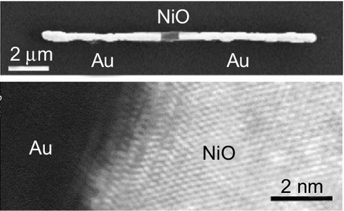
Figure 16.12 shows the I–V characteristics of individual Au–NiO–Au nanowire devices. The device showed the bipolar resistive switching. The voltage range was ≤ 6 V, whereas the current range was as high as a few hundred μA. These characteristics were similar to the unipolar resistive switching observed in the polycrystalline NiO nanowire device (Kim et al., 2008); thereby, the direct comparison with the report in single crystalline anionic memory is rather difficult. Also, the NiO segment length of 900 nm was achievable by the conventional lithographic technique. However, the methodology introduced in this section is still promising to reduce the operation voltage because the length of resistive switching segment can be scaled down to tens in nm scale by controlling the thickness of Ni during the electrochemical deposition. In fact, it was demonstrated that the voltage was reduced below 2 V by decreasing the length of NiO segment to 20 nm (Heber et al., 2012).

16.2.3 Resistive switching in a nanowire crossbar array
Although the oxide nanowire-based resistive memory was reviewed earlier, and the oxide nanowire was found to be a powerful tool to investigate the feasibility of resistive switching at the sublithographic scale range, the integration of these nanowires for a high-density memory device is a big challenge. Because two electrodes are required for addressing the target memory device independently, the total number of electrodes is estimated to be 2N, where N is the number of nanowire memory, which limits the density of memory integration. Nevertheless the number of electrodes can be reduced to N + 1 by wiring the multielectrodes on the nanowire. The footprint of individual memory cell is determined by the gap size between the electrodes, and therefore the number density of the memory device is still limited by the lithographic technique. The ultimate architecture for high-density memory can be achieved by the crossbar array, where the switching area is located at the junction of crossbar structure. The crossbar array architecture allows reduction of the number of electrodes down to (2N)0.5. To realize the crossbar array structure using oxide nanowires, two points must be addressed. First, the switching part should be only at the crossbar junction, whereas the other area should be electrically conductive. Second, the adjacent nanowires should be electrically isolated while keeping its conduction. In this regard, the metal-oxide core–shell nanowire structure may be promising to realize the crossbar array architecture (Figure 16.13).

Cagli et al. reported the proof of concept for the crossbar nanowire memory array (Cagli et al., 2011). They utilized the Ni–NiO core–shell nanowires fabricated by combining the AAO template method and the moderate thermal oxidization treatment. First, the Ni nanowires were fabricated by the electrochemical deposition of Ni in AAO template. Then the Ni nanowires with 200 nm diameter were aligned onto the silicon substrate with 150 nm thick SiO2 layer. Because Ni has a ferromagnetic nature, the orientation of Ni nanowires can be arbitrarily controlled by the external magnetic field (Figure 16.14). After aligning the Ni nanowires, the thermal oxidization treatment was carried out. The bottom nanowires were annealed at 300 °C for 3 h in air while the top nanowires were spontaneously oxidized at room temperature in air to avoid overoxidization of the bottom nanowires. Figure 16.14 also shows the transmission electron microscope (TEM) image and Ni–NiO core–shell nanowire and electron energy-loss spectroscopy (EELS) line profile. The presence of an amorphous NiO shell layer with a thickness of 15 nm was confirmed.


Figure 16.15 shows the device structure and the I–V characteristics of Ni–NiO nanowire crossbar junction (Cagli et al., 2011). The device shows the unipolar resistive switching continuously. The resistive switching at the crossbar junction was justified by analysing the local resistance of the nanowire crossbar device including the contact between nanowire and metal electrode (Table 16.2). Thus the proof of concept for the nanowire crossbar array memory was demonstrated. These results highlighted that the nanowire crossbar junction might be a promising approach to integrate the nanowire memory for high-density memory device applications.


Table 16.2
Local resistance analysis for nanowire crossbar junction
| State | Description of state | RAC (Ω) | RBD (Ω) | RAB (Ω) |
| 1 | Initial | > 107 | > 107 | > 107 |
| 2 | AC, BD forming | 180 | 326 | > 107 |
| 3 | AB forming | 180 | 326 | 265 |
| 4 | AB reset | 182 | 351 | 1.6 × 10⁷ |

Reprinted with permission from Cagli et al. (2011). © 2011 John Wiley and Sons.
In summary, the resistive switching in oxide nanowire was reviewed, covering the cationic memory and the anionic memory. Resistive switching was ensured at about the 10 nm scale and up to 108 cycles of endurance. Also, the low power consumption effect would be expected as a derivative of the scaling. Thus the review strongly supports the scaling of ReRAM down to the sublithographic scale to increase the density of memory device integration and the memory performance. Furthermore, the crossbar array using the metal-oxide core–shell nanowire was demonstrated as proof of concept for the high-density memory device. This result opens up opportunities for nanowire-based nonvolatile memory applications.
16.3 Oxide nanowire for exploring nanoscale mechanism of memory
Although ReRAM is known as a potential next-generation nonvolatile memory alternative to flash memory technology due to its excellent memory performance, unfortunately the mechanism of resistive switching has been controversial (Waser et al., 2009; Yang et al., 2008, 2012; Yanagida et al., 2013; Kwon et al., 2010; Valov et al., 2013). Because the nanoscale conducting filaments that govern the resistive switching phenomena are buried in the oxide matrix and the identification of the exact location of the conducting filaments is difficult, extracting the fundamental physical and chemical events in the conducting filaments has been quite difficult in conventional thin film devices. Oxide nanowire serves as a powerful tool to extract the fundamental mechanism of resistive switching by analysing the conductive filaments restricted into the nanowire structure. This section reviews the nanoscale mechanisms of resistive switching identified by using an oxide nanowire device. Especially the mechanism of the anionic resistive switching has been investigated. The oxide nanowire facilitates identification of the electrical properties, the chemical properties and the spatial information of the conducting filament, which had been impossible by conventional thin film device (Figure 16.16).

16.3.1 Chemical analysis of conducting filaments using oxide nanowire device
The chemical properties of conducting filaments can be evaluated by varying the surrounding atmosphere of the oxide nanowire device because the conducting filaments in the oxide nanowire are exposed to the environment and should sensitively interact with the ambient atmosphere. Nagashima et al. utilized the MgO–CoOx core–shell nanowire device to investigate the chemical properties of conducting filaments for the anionic resistive memory (Nagashima et al., 2011). The individual MgO–CoOx nanowire was electrically contacted with Pt electrodes. The reason why Pt was employed was to avoid the unexpected oxidization of electrodes, which makes the analysis complicated. The stable bipolar resistive switching in MgO–CoOx nanowire was confirmed by the endurance properties up to 108 cycles. To investigate the chemical properties of a conducting filament, first the resistance state of the device changed into the conductive ON state in air condition. Then the chamber was evacuated to 10− 2 Pa within 2 min, followed by the introduction of reactive gas. Prior to the measurement, the pressure of reactive gas was controlled to be 10− 1 Pa and kept for 5 min. Because the electrical transport in oxides is known to be varied by the concentration of oxygen, a redox might affect the mobile carries of oxides, and the experiment using redox gases enables identification of the conducting properties of resistive switching. On the basis of the earlier hypothesis, the effect of reactive gas such as O3 (7% in O2), pure O2, dry air (20% O2 in N2) and H2 (4% in Ar) for the conduction properties was examined. Figure 16.17 shows the retention measurement in the reactive gases. The reading of the nanowire resistance was performed only at the data points shown in the figure to avoid the unintentional resistive switching during measurement. The readout voltage was 2 V. Interestingly, the conduction of MgO–CoOx nanowire tended to be enhanced when O3 contained oxidization gas was introduced, whereas H2 contained reduction gas suppressed the conduction. The conduction properties of MgO–CoOx nanowire were found to vary systematically corresponding to the ability of the redox reaction of gases. Because cobalt oxide is known to show the p-type carrier transport where the conduction is caused by the cation deficiency or the excess oxygen, the trend observed in the retention measurement was consistent with the p-type transport nature of cobalt oxide (Wdowik and Parlinski, 2008; Hed, 1969; Shinde et al., 2006).

Similar experiments were reported in MgO–NiO core–shell nanowire and MgO–TiO2 core–shell nanowire (Oka et al., 2010; Nagashima et al., 2012a). The results showed that the trend in MgO–NiO nanowire was almost same as MgO–CoOx nanowire. In contrast, MgO–TiO2 showed the opposite trend, that is, the H2 contained reduction gas enhanced the conduction, but the O3 contained oxidization gas strongly suppressed the conduction. Because NiO and TiO2 are p-type and n-type oxides, these results were rational. Although the results from the atmosphere control measurement seems to be natural and not so surprising from the aspect of oxide electronics, these results demonstrated the significance of the redox event on the resistive switching and gave one answer for the discussion on the controversial conduction mechanism of anionic resistive switching. More practically, the knowledge provides the logical pathway to design the nanoscale ReRAM.
16.3.2 Electrical analysis of conducting filaments using oxide nanowire device
The planar structure of an oxide nanowire memory device offers the unique analysis tool to evaluate the electric properties of conducting filaments. Figure 16.16 shows a schematic of the oxide nanowire FET device to analyse the carrier type in the conducting filaments. The electrical transport of the oxide nanowire memory is in principle modulated by the electric field from the gate electrode. This methodology is difficult to be taken in a conventional thin film device due to the difficulty in introducing the gate electrode near the conducting filaments. The carrier property of resistive switching was directly evaluated by Nagashima et al. using MgO–CoOx core–shell nanowire FET device (Nagashima et al., 2011). Figure 16.18 shows a scanning electron microscope (SEM) image of the MgO–CoOx nanowire FET on the silicon substrate covered with 300 nm SiO2. Pt was utilized as contact electrodes. The gap size between source (S) and drain (D) was about 400 nm.

Prior to the FET measurement, the device was set into the conductive ON state with the compliance current of 10− 9 A. After confirming the small distribution of conduction within 0.3 × 10− 10 A at 15 V, the measurement was carried out. When the positive + 8 V (VG) was applied to the gate electrode, the source–drain current (ISD) decreased, whereas ISD increased for the negative − 8 V. The detailed trend could be seen in the transfer curve (ISD–VG) as shown in the inset of Figure 16.18b, clearly showing that ISD increased as the gate voltage decreased. These results indicated that the electrical conduction in bipolar resistive switching of CoOx is governed by the p-type carrier transport, which was consistent with the result of chemical properties analysis discussed earlier (Nagashima et al., 2011). Thus the oxide nanowire was found to be able to utilize as an analysis tool to evaluate the carrier transport of the resistive switching.
16.3.3 Spatial analysis of conducting filaments using oxide nanowire device
Identifying the exact location of resistive switching is one of the important clues to understanding the mechanism of ReRAM because it is related to the generation and the evolution of conducting filaments. Previously, the switching location was evaluated by investigating the effect of anode/cathode electrode material on the resistive switching event (Seo et al., 2005; Lee et al., 2007, 2008). However, such an evaluation method contains a serious problem, that is, the switching location would be changed when the electrode such as Ti, Ag and Al is oxidized, and the electrode/oxide interface governs the resistive switching. To avoid this problem, the direct identification of switching location using a planar-shaped nanowire device might be promising. Nagashima et al. applied a multiprobe measurement to identify the switching location of bipolar resistive switching in p-type cobalt oxide (Nagashima et al., 2011). Several Pt electrodes were contacted on the MgO–CoOx core–shell nanowire as shown in Figure 16.19.

The location for resistive switching was examined by using three electrodes, namely electrode A, electrode B and electrode C in the figure. First, the forming process was performed between electrodes A–C, where the voltage was applied to electrode A while electrode C was grounded. After the forming process, the device showed the bipolar resistive switching as shown in Figure 16.19b and Table 16.3. The local resistance change was monitored before and after the resistive switching via the intermediated electrode B. Clearly, the resistance change between electrodes B and C (cathode side) was larger (ON/OFF ratio ~ 17.1) than that between electrodes A and B (anode side; ON/OFF ratio ~ 2.2), indicating that the resistive switching of cobalt oxide occurred at the cathode side. Although the switching location in n-type oxide, of which the conduction mechanism is based on the oxygen vacancies, had been known to be the anode side (Yang et al., 2008; Kwon et al., 2010), the switching location in p-type oxide was demonstrated for the first time using oxide nanowire. Taking into account the carrier generation mechanism of oxides, the opposite switching location between n-type and p-type oxides can be rationally understood.
Table 16.3
Summary of the resistances for each area highlighted in Figure 16.19
| Measured area | ON state resistance (Ω) | OFF state resistance (Ω) | ON/OFF ratio |
| A(anode)–C(cathode) | 2.06 × 10¹⁰ | 3.02 × 10¹¹ | 14.7 |
| A–B(anode side) | 4.74 × 10⁹ | 1.06 × 10¹⁰ | 2.2 |
| B–C(cathode side) | 1.20 × 10¹⁰ | 2.05 × 10¹¹ | 17.1 |

Reprinted with permission from Nagashima et al. (2011).
© 2011 American Chemical Society.
The switching location of p-type oxide was also reported by Oka et al. using NiO nanowire (Oka et al., 2011). They utilized the asymmetric SiO2 passivation layers onto NiO nanowire devices. The four types of the devices were prepared such as NiO nanowire device (Type I) passivated at anode side, (Type II) passivated at cathode side, (Type III) without passivation and (Type IV) fully passivated as shown in Figure 16.20. The I–V characteristics of the NiO nanowire device without passivation showed a symmetric bipolar resistive switching, whereas the fully passivated NiO nanowire device showed an asymmetric bipolar resistive switching. The prominent passivation effect was confirmed only when the cathode side was passivated, obviously indicating that the resistive switching occurred at cathode side. Although the role of passivation effect on the resistive switching was not well understood, these results highlighted that the switching location of bipolar resistive switching in p-type oxide commonly occurred at cathode side.


Thus, the methodology using oxide nanowire offered the powerful tool to identify the location of resistive switching. The extracted information on the switching location is very important not only to understand the underlying mechanism of resistive switching but also to design and improve the performance of ReRAM.
16.3.4 Stability of resistive switching in nanoscale resistive memory device
As the cell area scales down to nanometer, the size of conducting filaments becomes comparable to the device size, and the interaction with the surrounding atmosphere must be increasingly crucial for the performance of ReRAM. The electrically programmed resistance state should somehow survive by competing with the surrounding atmosphere for the nonvolatility. Such knowledge is rather important to design the resistive switching at nanoscale and therefore toward the high-density ReRAM. However, such interaction with surroundings had not been accessible due to the limitation in conventional lithography.
Nagashima et al. investigated the role of the surrounding atmosphere on the stability of nanoscale resistive switching (Nagashima et al., 2012b). They prepared the planar-type resistive memory devices utilizing several oxide nanowires, including TiO2 − x nanowire (n-type), MgO–NiO nanowire (p-type) (Oka et al., 2010) and MgO–CoOx nanowire (p-type) (Nagashima et al., 2010a, 2011). The TiO2 − x nanowires were fabricated onto SiO2/Si substrate by combining PLD and electron beam lithography (Nagashima et al., 2012b). The deposition of TiO2 − x was performed at room temperature in 10 Pa of oxygen pressure. The thickness and width of TiO2 − x nanowire were 80 and 100 nm, respectively. The fabrication of MgO–NiO nanowire and MgO–CoOx nanowire was similar to that in Section 16.2. The oxide nanowires were electrically contacted with Pt electrodes, of which the gap size was 200 nm.
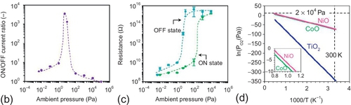
Figure 16.21 shows the I–V characteristics and the retention data of planar structured oxide nanowire devices measured at room temperature in air. The TiO2 − x nanowire didn’t exhibit a resistive switching, whereas the MgO–NiO nanowire and the MgO–CoOx nanowire clearly showed the bipolar resistive switching with 104 s of retention. Because the bipolar resistive switching in TiO2 thin film devices was reported (Nagashima et al., 2012a), no switching behaviour in TiO2 − x nanowire might be caused by the interaction with surrounding atmosphere. Therefore, the surrounding condition was varied by changing the pressure of the measurement chamber. Figure 16.22 shows the I–V characteristics of TiO2 − x nanowire devices measured under various ambient pressures. Interestingly, the hysteresis of I–V curves tended to increase as the pressure was reduced to 1 Pa and the clear bipolar resistive switching was seen. Further reducing the ambient pressure resulted in the decrease of hysteresis. The ON/OFF current ratio and the resistances of ON state and OFF state as functions of ambient pressure were shown in Figure 16.22b and c, respectively. The ON/OFF current ratio was found to have a maximum value at 5 Pa. Because it is well known that the oxygen vacancies act as a donor for the electrical conduction in n-type oxides, the results could be interpreted in terms of the amount of oxygen vacancies. These results demonstrated that the resistive switching can be stably performed in nonstoichiometric TiO2 − x between stoichiometric insulative TiO2 and highly conductive TiO2 − x with plenty of oxygen vacancies. In the thermodynamic diagram of oxides, the equilibrium line of TiO2 is located much below the atmospheric oxygen pressure. Therefore, the interaction with surrounding air condition strongly drives TiO2 − x back to stoichiometric TiO2. On the other hand, the equilibrium lines of NiO and CoO are close to the atmospheric oxygen pressure, enabling the stable resistive switching in air condition because the driving forces to drive back to the stoichiometric state for NiO and CoO should be much smaller than that for TiO2. Although the dynamic reaction at the grain boundaries and the surface of oxides cannot be captured quantitatively, the discrepancy between TiO2 − x, NiOx and CoOx on the resistive switching at atmospheric pressure should be qualitatively significant. Furthermore, the results in TiO2 − x implied that it is important to design the surrounding condition, for example, via the passivation layer, toward the highly stable nanoscale ReRAM.


The impact of the passivation layer on the stability of resistive switching was examined in the TiO2 − x nanowire device. Amorphous SiO2 with 300 nm thickness was selected as the passivation layer because the diffusion of oxygen in SiO2 is much slower than that in air. Figure 16.23 shows the device structure and the electrical characteristics of the SiO2 passivated TiO2 − x nanowire device. The measurement was performed under atmospheric conditions. In contrast to the I–V curve of the bare TiO2 − x nanowire device as shown in Figure 16.21, the passivated device clearly showed the bipolar resistive switching. The endurance was stably repeated until 106 cycles. Although further investigations need to be undertaken to realize a much higher stability of resistive switching, these results strongly encourage tailoring a resistive switching at nanoscale.

16.3.5 In situ analysis of resistive switching using transmission electron microscopy
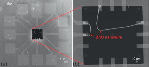
As discussed earlier, the oxide nanowire structure enables identification of the mechanism of resistive switching more directly than conventional thin film form. However, these investigations are still indirect, and the dynamic behaviours of resistive switching cannot be captured. In situ analysis combining the electrical measurement and the TEM observation is elegant solution. Huang et al. reported the in situ analysis of resistive switching using ZnO nanowire device (Huang et al., 2013). In this report, ZnO nanowires were fabricated by a VLS mechanism in the furnace. The diameter and the length of ZnO nanowires were 100 nm and 5 μm, respectively.
The TEM specimen for in situ analysis was constructed via the photolithography and electron beam lithography. First, 30 nm SiO2 and 60 nm Si3N4 were deposited on silicon substrate by low-pressure CVD. A window for TEM observation was then created via the reactive ion etching by removing the SiO2 and the Si3N4 layers, followed by the silicon etching through KOH chemical etching. After creating the window, the conventional lithography was applied to make an electrical contact with Ti/Au electrodes as shown in Figure 16.24.
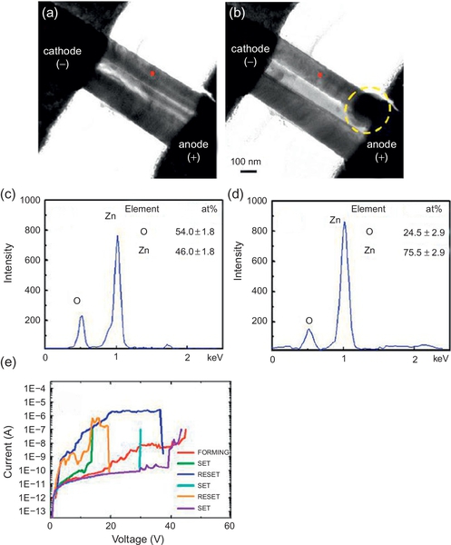
The electrical measurement of ZnO nanowire was conducted in the TEM chamber. Figure 16.25 shows the series of TEM images taken from video when a positive voltage of 3 V was applied to the electrodes. Interestingly, the portion near the anode tended to expand after the SET process (resistive switching into conductive state). This trend was reproducibly observed in the Au/ZnO nanowire/Au device structure. Figure 16.26 shows another sample of the ZnO nanowire memory device composed of two ZnO nanowires between electrodes. The device continuously showed the unipolar resistive switching after a forming process. Similar to the image in Figure 16.25, the portion near the anode expanded after the SET process. The composition analysis was then performed to identify what changed during the resistive switching process. Energy dispersive spectroscopy (EDS) analysis in Figure 16.26c and d exhibits the compositional change at the middle area of ZnO nanowire during the resistive switching. In the virgin state, the Zn/O ratio was almost 1 (Zn:O = 46.0:54.0 at.%) as shown in Figure 16.26c. When the SET process was performed, the Zn/O ratio increased (Zn:O = 75.5:24.5 at.%), indicating that the oxygen vacancies were induced via the SET process. Contrary, the Zn/O ratio returned to be almost 1 (Zn:O = 42.6:57.4 at.%) after the RESET process (resistive switching into insulative state). These results supposed that the formation and rupture of the oxygen vacancies-based conducting path were crucial for the resistive switching phenomena in ZnO. EDS mapping near the anode further evidenced the dynamic migration of oxygen during the resistive switching (Figure 16.27). After the SET process, the Zn/O ratio near the anode was much higher than the virgin state (Zn:O = 9.4:90.6 at.%). These results give us an important clue to understand the dynamic mechanism of resistive switching. First, the oxygen was decomposed to oxygen vacancies and oxygen ions through the electrical breakdown process. Because the oxygen ions are negatively charged, the oxygen ions migrated toward the anode side under the electric field, leaving the oxygen vacancies based conducting path. This caused the low resistance, conductive ON state. The electrode should have an ability to restore the oxygen ions to exhibit nonvolatility. In the RESET process, the oxygen ions solely cannot be driven back from the anode under the electric field because the polarity of bias for SET and RESET processes was not changed in unipolar switching. The complementation of oxygen vacancies during the RESET process might be achieved by the removal of oxygen ions from the anode with the assist of Joule heating. Consequently, the conducting path was ruptured and the insulative state obtained with the stoichiometric composition of ZnO. Thus, the in situ analysis combining the electric measurement and TEM/EDS observation on oxide nanowire device was demonstrated as a powerful tool to capture and extract the intrinsic nature of conducting path for the full understanding of the resistive switching mechanism.


In summary, this section reviewed the mechanisms of ReRAM, which is especially for the anionic resistive switching, extracted by the oxide nanowire device. The oxide nanowire offered unique analysis tools, which had never been accessible by the conventional thin film device form. The carrier type of the conducting filaments was identified electrically and chemically by using the nanowire FET structure and the atmosphere controlled measurement, respectively. Also the location of resistive switching could be analysed via the multiprobe measurement and the asymmetric passivation technique. The interaction with surrounding atmospheres gave a fundamental understanding for the emergence of nonvolatility in oxide-based resistive switching. The in situ analysis combining the electric measurement and the TEM observation enabled evaluation of the dynamics of resistive switching phenomena. The results obtained from the oxide nanowire device revealed the new aspects of the resistive switching and allows one to tailor the performance of nanoscale ReRAM.
16.4 Perspective
In this chapter, the significance of oxide nanowire for investigating the potential scalability and the fundamental mechanisms of resistive switching were discussed. The chapter demonstrated that the oxide nanowire devices gave us the fruitful wisdom to understand fully and tailor the nanoscale resistive switching system. Also, the bottom-up nanowires have the structural uniqueness that is difficult to be realized by the conventional lithographic technique, offering the platform of oxide nanowire-based nonvolatile memory applications. However, there are several challenging issues to be addressed for the breakthrough of nanowire memory applications as discussed next.
First, the nanowire/electrode contact should be ensured for stable resistive switching. The importance of nanowire/metal interface on the transport properties of oxide nanowire has been discussed (Léonard and Talin, 2011; Nagashima et al., 2010b). When the contact resistance exists in the oxide nanowire device, the applied voltage drops at the interface, and the substantial voltage to the memory cell becomes small, resulting in the large operation voltage. Furthermore, when the contact resistance is much higher than the resistance of memory cell, the resistance change of the memory cell is buried in the circuit resistance. Because the metal/oxide interface was found to affect the resistive switching event (Seo et al., 2005; Lee et al., 2007, 2008), the precise control of nanowire/metal interface would be important to exploit the full potential of oxide nanowire.
Second, the structural uniformity of bottom-up oxide nanowires should be acquired. Generally, the bottom-up oxide nanowire has the structural distribution that comes from the inhomogeneous nucleation formation at initial state of nanowire growth. Because the conduction of nanowire is proportional to the cross-sectional area (i.e., πr2), where r is the radius of nanowire, the size distribution of the nanowire radius causes the wide variation in nanowire resistance. The grain boundaries in polycrystalline nanowire form are also the factor of the variation in nanowire properties. As the nanowire size becomes small, the number of grain boundaries is limited. Because the grain boundaries are well known to influence the transport property of semiconductors, the difference of the number of grain boundaries between nanowires also yields the variation in the conduction property. Thus, controlling the distribution not only in nanowire size but also in grain boundaries is quite important for realizing the homogeneous device performance.
Third, the passivation of nanowire memory devices should be designed to stabilize the resistive switching phenomena. Because the importance for maintaining the nonstoichiometric state of oxide on resistive switching was discussed in last section (Nagashima et al., 2012b), designing the passivation layer by taking into account the oxygen affinity is crucial to develop the robust, reliable and high-performance nanowire nonvolatile memory.
Fourth, the postgrowth alignment of oxide nanowires is necessary to integrate the nanowires into desired electric circuit. Because the bottom-up grown nanowires are randomly distributed on the growth substrate, a technique of postgrowth alignment of nanowires on desired substrate is a common inevitable issue for the research of bottom-up nanowires. Especially, for the nonvolatile memory applications, each oxide nanowire should be individually connected to electrodes, and adjacent nanowires should be electrically isolated. On this point of view, a nanowire alignment method using a water/oil interface demonstrated by Nakagawa et al. might be promising to satisfy this requirement (Nakagawa et al., 2008). In this method, the hydrophilic/hydrophobic patterned substrate was prepared. When water was coated over the substrate, the water was placed only onto the hydrophilic surface. Then the nanowire suspended 1,4-dichlorobutane (oil) was coated, and the clear water/oil interface was created. Because the nanowire surface was chemically modified to minimize the Gibbs’ free energy at the water/oil interface, the nanowires were selectively captured at the interface (i.e., prepatterned hydrophilic surface). The yield of nanowire alignment was around 99%. However, it is still challenging to align the nanowires precisely at the desired position with low crossing defect density. Another impressive method for individual nanowire alignment technique was demonstrated by Yao et al. (2013). It is the so-called nanocombing alignment technique. They partially anchored the nanowire onto the substrate, then draw out over the chemically modified nonadhesive surface. The yield of nanowire alignment and the tilting angle were 98.5% and within ± 1%, respectively. The arrays have a crossing defect density of ~ 0.04 nanowires per micrometer. Also, the method allows aligning the millimeter long nanowires, and the nanowires were able to be uniformly trimmed to the same length after the alignment. Furthermore, the integration of the nanowires in the form of cross-bar array was demonstrated. Inherently, the methodology was applicable to any substrate surface, strongly encouraging the nanowire-based unique device applications.
Finally, the possible application fields of oxide nanowire-based nonvolatile memory were discussed. Although the nanowire alignment methods discussed earlier gave a big impact for the nanowire research field, the bottom-up nanowire in principle cannot overcome the top-down devices on its memory density as long as the lithographic technique is utilized for the nanowire alignment process. Even the densely packed nanowire array could be achieved by self-assembling technique (Whang et al., 2003); an electrical contact to individual nanowire should be defined by the lithographic technique.
One possible way for the oxide nanowire memory to overcome the top-down memory is to apply the oxide nanowire memory to the flexible electronic systems where the top-down memory is unfeasible. Flexible electronics is an emerging field in electronics and is intensively investigated for the portable and wearable electronic system (Nathan et al., 2012; Son et al., 2014). A flexible nonvolatile memory is an important component for the self-standing devices. In fact, many efforts have been devoted to synthesize the flexible memory (Kim et al., 2011; Cheng et al., 2011; Han et al., 2013). Due in strength of material, a strain is calculated by the equation ɛ = y/ρ, where y is the distance from the neutral surface and ρ is curvature radius, a small diameter of the nanowire is beneficial for being bent with small strain. In addition, the single crystalline nature of nanowires further encourages the flexible device applications due to the lack of mechanically weak grain boundaries. Thus the oxide nanowires are promising nanomaterial for flexible nonvolatile memory applications. Especially in wearable devices for monitoring the health of humans in the dairy life, the nonvolatile memory may be utilized for storing temporary information before transferring to the analytic device. In this case, the memory capacity of the health monitoring device doesn’t have to be as large as that of conventional information storage. Therefore, the flexible health monitoring device may be one of the solutions to take full advantage of the nanowire-based nonvolatile memory.