
Multiferroic and heterogeneous ferromagnetic nanowires prepared by sol–gel, electrodeposition, and combined techniques
L.A.S. de Oliveira1; R. López-Ruiz2; K.R. Pirota2 1 Universidade Federal do Rio de Janeiro, Rio de Janeiro, Brazil
2 Universidade Estadual de Campinas, Campinas, Brazil
Abstract
This chapter will give a concise review of the fabrication methods of multiferroic and heterogeneous ferromagnetic nanowires. First, a general overview about nanowire synthesis is presented. In the context of an alumina membrane template-assisted method, we present the approaches to modulate the geometry or the composition of ferromagnetic nanowires by electrodeposition. In the same way, sol–gel methods can produce more versatile compounds as multiferroic materials (when two or more ferroic properties coexist in the same phase, namely, ferroelectricity, ferromagnetism, or ferroelasticity). They possess great potential for sensor applications as well as open several branches of fundamental science research. Finally, the fabrication of other structured nanowires composed of both ferromagnetic and multiferroic phases by combined techniques is presented.
3.1 Introduction and background
A key in the competitive development in this century will be, undoubtedly, the development of products with a wide range of functional aspects. In this context, multifunctional materials known as smart materials will play a decisive role (Gandhi and Thompson, 1992). Among many other systems, multiferroic materials stand out for their great applicability.
Ferroic is the generic name for a material that exhibits ferromagnetic, ferroelectric, or ferroelastic behavior. A characteristic spontaneous magnetization, electric polarization, or strain appears, respectively, on those materials (Wadhawan, 2000). A material is called multiferroic when two or more of these ferroic properties coexist in the same phase, namely, magnetoelectricity (ferromagnetism and ferroelectricity) (Bichurin and Wiehland, 2012), magnetostriction (ferromagnetism and ferroelasticity) (Gibbs, 2000), or piezoelectricity (ferroelectricity and ferroelasticity) (Taylor, 1985).
The present increasing need for miniaturization of electronic devices and the great advances in nanotechnology and materials engineering allow us to manufacture multiferroic-based devices at the nanoscale. At this size range, the objects exhibit new physical properties different from the bulk analogs (Stefanita, 2008). These new properties have attracted the attention of the scientific community due to the emergence of new effects that could expand the technological applications. Because of their properties, which are particularly dependent on the dimensionality, several studies of 1-D nanostructures have been performed. Thus, there is an increasing interest in the synthesis of nanowires (He and Tao, 2004), nanorods (Tien et al., 2008), nanotubes (Daub et al., 2007), or nanobelts (Wang, 2004), linked to the study of these low-dimensional systems.
The nanowire is a model in the study of the size-confinement and surface effects on the magnetic, electrical, or optical behavior (Liz-Marzán and Giersig, 2003). For instance, exotic new magnetic and electric polarization states like helical antiferromagnetism can be present in this scale due to geometric frustration and breaking of the long-range coupling (Young et al., 2014). Also, in this scale, novel quantum effects associated with 1-D singularities in the electronic density of states can be observed. On the other hand, 1-D nanostructures have a great appeal in technologies as sensors (Patolsky et al., 2006), high-density magnetic storage media (White, 2000), optics (Agarwal and Lieber, 2006), or electronic technologies (Capasso and Datta, 1990). Furthermore, they can be part of components in devices and nanocircuits (Yan et al., 2014). To fabricate such structures, the template-assisted methods have been revealed to be conceptually simple and effective (He and Tao, 2004). These templates usually contain cylindrical pores, with diameters of tens or hundreds of nanometers, which act as the negative of the desired material. The most used template is probably anodized aluminum oxide (AAO). Its versatility has been proven in the manufacture of materials with different morphologies (nanowires, nanotubes, or antidot thin films) or compositions (inorganic, organic, or inorganic–organic hybrids). Although disordered AAO membranes were used to embed magnetic materials (Keller et al., 1953; Huysmans et al., 1988) a long time ago, the fabrication of nanowires using AAO as a template became common only after Masuda’s group published the conditions to produce a self-ordered regular nanoporous structure in alumina in 1995 (Masuda and Fukuda, 1995). Nevertheless, the achievement of an AAO template had come earlier, in 1989 (Furneaux et al., 1989). After the subsequent use of AAO as filters or masks (Masuda and Satoh, 1996), there has been an increased interest in the tuning of such nanostructures with controlled morphology parameters as pore diameter or interpore distance.
In order to fill the template, several strategies can be employed. An AAO template allows the use of many different techniques to fill up the pores. A widely used technique is electrochemical deposition or electrodeposition. Ferromagnetic nanowires were fabricated by electrodeposition a long time ago for decorative purposes (Wernick et al., 1987), and nowadays there are simple techniques to build inhomogeneous wires modulated along their length in diameter or composition. Also, alloy nanowires can be produced, see for instance (Fei et al., 2007). By means of the sol–gel chemical route, high-purity nanoparticles, in particular oxides of magnetic materials as ferrites or perovskites, have been obtained. The sol–gel technique creates the possibility to fabricate oxide magnetic nanowires (Pechini, 1967), particularly interesting for their multiferroic properties, as was published very recently in de Oliveira and Pirota (2012).
First, this chapter will focus on the preparation of template-assisted heterogeneous ferromagnetic nanowires modulated in geometry or composition by means of conventional electrodeposition filling. Also, sol–gel nanowire production is presented. Finally, we pay special attention to the combination of the two so-called fabrication methods, sol–gel and electrodeposition. This combination allows for the fabrication of core–shell metallic or insulating structures. In these heterogeneous materials, in which metal or insulator components can be placed in both core or shell parts, the individual properties of each constituent can become quite different. Also, possible exchange relations (e.g., exchange bias, exchange spring) or ferroic coupling (e.g., magnetoelectricity induced by mechanical stress) makes them especially interesting. Also, ferromagnetic–multiferroic combinations inside the wire can be produced.
3.2 Nanowire synthesis: A general overview
A general overview of the synthesis of nanowires is sketched in Figure 3.1. Besides top-down lithographic methods, which are out of the scope of this chapter, bottom-up synthetic methods are presented. Although, in some cases, direct reactions will give rise to nanowire structures (Sun et al., 2002; Yu et al., 1997), in a surfactant organized media or positive-template mediated in DNA chains (Mbindyo et al., 2001) or carbon nanotubes (Fullam et al., 2000) in solution, most nanowires are produced by template-assisted methods. The essential features of a good template are chemical stability, the mechanical properties, and homogeneity of the pore ordering, namely, density and diameter. Block co-polymer templates are based on the synthesis of a structure of two noncompatible monomers that tend to be self-organized in macroscopic structures as lamellas or cylinders. In the last case, a selective removal of the cylindrical monomer phase gives rise to a porous polymer template. The most well-known system is the polymethylmethacrylate/polystyrene (Thurn-Albrecht et al., 2000a,b). In the track-etched membranes, a nonporous substrate, mica (Sun et al., 1999, 2000) or a polymer (polycarbonate or polyester) (Ferre et al., 1997), is bombarded with an ion beam in order to create damaged tracks. The membrane formed can be chemically etched to obtain the desired pores (Fleisher et al., 1975). Although the resulting pores have a uniform diameter, the drawback of this technique resides in the lack of porous ordering. The porous alumina membranes are also widely used and will be extensively described in the following text. After the porous template is created, in addition to metals, several materials can be grown inside the pores, for instance, polymers (Martin et al., 1993), semiconductors (Lakshmi et al., 1997), carbon (Manoharan, 2009), oxides (Wang et al., 2007), or intermetallic materials (Huang et al., 2002).

3.3 Advanced heterogeneous ferromagnetic nanowires by electrodeposition
AAO membranes are usually fabricated from a high-purity aluminum foil by the well-known two-step anodization process (Masuda and Fukuda, 1995). The resulting structure is a honeycomb in which a scalloped oxide barrier layer separates the porous zone and the sustaining aluminum. Highly ordered pore arrangement with narrow size distribution is obtained for some optimum values of voltage and temperature (Nielsch et al., 2002) or via previous prepatterning methods such as imprint lithography (Choi et al., 2003a) or e-beam lithography. In order to control the temperature, a specially designed electrochemical cell is usually required.
The field-assisted alumina solution at the electrolyte–oxide interface (bottom of the pore) is compensated by oxide growth at the oxide–metal interface (Parkhutik and Shershulsky, 1992); the pores grow downward, arranging with time in a regular array. Although the true reason for the self-ordering is still unknown, in Jessensky et al. (1998) it was suggested that the mechanical stress, which is associated with the expansion of the aluminum during oxide formation, is the cause of repulsive forces between neighboring pores during the oxidation process and leads to self-organized formation of hexagonal pore arrays. Other explanations have been proposed (Pashchanka and Schneider, 2011; O’sullivan and Wood, 1970; MacDonald, 1993).
In order to reduce the time and manipulation that are required for double anodization, great advances have been achieved using nanoimprint and lithographic techniques before anodization (Asoh et al., 2001) (see Choi et al., 2003b, for substrates different than Al). Nanostructured titanium nitride (TiN) molds have recently been developed (Navas et al., 2007), following the procedure described in Figure 3.2. TiN thin films were grown by reactive magnetron sputtering using a Ti target (99.995% purity) on different AAO membranes as substrates (Figure 3.2a). In all cases, the mean thickness of the plain TiN films is 0.7 μm, controlling the deposition rate. Ti layers of around 1 μm were sputtered to achieve a larger stability, and an aluminum/alumina specimen can be detached by means of selective chemical etching as described in Pirota et al. (2004). The TiN films and the Ti/TiN bilayer were attached to a silicon wafer to facilitate the manipulation (Figure 3.2b).

Prepatterned aluminum can be obtained by applying pressure with the nanoimprint tool (Figure 3.2c). Finally, with this mechanically puckered aluminum, only one anodization is needed to obtain highly ordered AAO membranes without the tedious anodization/removal puckering described in the two-step anodization process. Due to their great hardness and chemical passivation, the TiN molds can be used several times and without corrosion. An atomic force microscope (AFM) image of a typical prepatterned Al foil is shown in Figure 3.2d.
It is quite interesting and easy to produce structures with variable diameters but that have the same distance between wires via wet etching. After the widening process is calibrated by rinsing in a phosphoric acid solution, the later filling gives rise to systems that can be used as a model to evaluate dipolar effects. A typical scanning electron microscopy (SEM) image from a widened AAO surface fabricated from an original 35 nm diameter pore is shown in Figure 3.3.

3.3.1 Geometry modulation
3.3.1.1 By pore widening and third anodization
The combination of the conventional growth of alumina and pore chemical widening (procedure in Figure 3.4) allows researchers to produce templates in order to get double-diameter nanowires, which are important for thermoelectric energy conversion (Zianni, 2010) and for computing purposes (Parkin et al., 2008). Basically, the Al is anodized in two steps, and the resulting template is pore-widened in accordance with the processes explained before (steps a–e). The third anodization (step 5) produces the bottle-neck and the diameter modulation of the pore (f). See an SEM micrograph of a modulated-diameter sample in Figure 3.5. The geometry of the pores can be easily manipulated via the anodization voltage, etching widening time (step 4 of Figure 3.4), and the second/third anodization time ratio (steps 3 and 5 of Figure 3.4).


3.3.1.2 By hard-mild anodization change
Essentially in a conventional anodization, as the electrolyte acid force increases, the applied voltage has to be reduced in order to prevent vigorous fizzing and strong heat emission. When this occurs, the alumina becomes yellow and sequentially darker, giving rise to a disordered and cracked alumina coating (Wernick and Pinner, 1972). This “hard” anodization, used in the industry since the 1960s with a high current density in an electrolyte at zero or negative temperatures, has been recently developed for research purposes by Lee et al. (2006), producing the so-called honeycomb structure. To stabilize the fast growth rate requires (1) the use of a specially designed cell in order to mitigate the large amount of heat generated and (2) the previous growth, before start the hard anodization, of a low-voltage coating alumina. In this system, the growth rate of the alumina layer increases drastically, avoiding the necessity of manipulation and the time-consuming double anodization. In Figure 3.6, we can observe the pore diameter variation with the applied voltage in this system. Samples reveal lower porosity values: 3–4% in contrast to the 10% that is expected using conventional conditions. Interestingly, for the conditions in which the interpore distance is equal in both systems, the hard anodization process produces narrower pores. This fact can be used to modulate the pores exchanging the anodization conditions (Lee et al., 2006).

3.3.2 Composition modulation
Electrochemical deposition is the most common tool used to fill the membranes in order to produce nanowires. For instance, nickel nanowires are usually deposited from the Watts bath electrolyte (Watts, 1916). To apply this technique in an AAO template, it is necessary to remove (Fert and Piraux, 1999) or decrease the thickness of the isolating barrier layer that separates the pore ending and the metallic Al electrode. A good method is presented in Cheng et al. (2007) by means of formation of a dendritic pore structure at the pore’s end using an exponential decrease of the anodization potential. It is quite versatile, and it allows for the deposition of metals (e.g., Co, Cu, Fe, Bi, Ag, and Au), polymers (Martin, 1994), superconductors (Pang et al., 2002), semiconductors (Mondal, 2007), and heterostructures (e.g., Cu/Co) (Fert and Piraux, 1999). The electrodeposition of metals can be done in DC (Fert and Piraux, 1999), AC (Metzger et al., 2000; Li et al., 1998; AlMawlawi et al., 1991), or current–voltage pulses (Tang et al., 1995; Nielsch et al., 2000).
Another way to modulate ferromagnetic nanowires is the fabrication of in-composition multisegmented nanowires. It can be done via two different procedures. The first one consists of a potential selective method, in which the two metals are in the same solution. By switching between the redox potentials of the two constituents, multisegmented composition nanowires can be produced. As opposed to conventional nanowires, this method requires the use of a three-electrode cell (Piraux et al., 1994; Blondel et al, 1994; Liu et al., 1995; Dubois et al., 1997; Wang et al., 1996). The second way is to perform sequential depositions using two different electrolytes (Blondel et al., 1997; Pirota et al., 2005). Using this approach, ferromagnet/insulator/ferromagnet multilayers for magnetoresistive tunnel junctions have been successfully grown (Liu et al., 1995).
3.4 Nanowires prepared by the sol–gel technique
3.4.1 The sol–gel technique
Sol–gel is probably the most versatile technique employed to produce nano-phased materials, and it has been extensively used since the mid-1800s (Hench and West, 1990). Generally, it starts with atomic or molecular precursors, allowing for control of the structure on the nanoscale from the earliest stages of the process, having lower distribution in the final particle size. Some advantages compared with conventional ceramic processes are high homogeneity, high phase purity, and lower processing temperatures. The sol–gel technique is defined as a colloid, that is, a dispersion of solid particles with diameters ranging from 1 to 100 nm in a liquid, in which, after some process, the particles become interconnected, forming a rigid network with pores of submicrometer dimensions or polymeric chains (Brinker and Scherer, 1990).
The whole sol–gel process can be divided into several steps as explained below:
Mixing: After selecting and weighing the precursors, they are diluted and mixed together, under constant stirring. At this first step, colloidal particles, with diameters that range from 1 to 100 nm, are dispersed in a liquid medium with a controlled pH, in order to prevent the precipitation of the different constituents. During this step, while mixing occurs, hydrolysis and polycondensation reactions initiate at numerous sites within the solution. When sufficient interconnected bonds are formed, the reaction mixture starts to respond cooperatively as colloid particles or as sol. The size of these sol particles depends on several variables, for instance, pH or alkoxide precursor/H2O or alcohol ratio, not discussed here.
Casting: Under usual conditions, the sol is a low-viscosity liquid that can be cast into a template for subsequent solidification in order to fabricate nanowires or nanotubes. The template must be well selected to avoid gel adhesion.
Gelation: With time the colloidal particles link together by physical or chemical interactions, forming a three-dimensional solid network containing liquid trapped in the interstices (Iler, 1979). Figure 3.7 shows a schematic view of gels formed by physical (Figure 3.7a) and chemical interactions (Figure 3.7b), giving rise to a colloidal or a polymeric system, respectively. There are several physical interactions that maintain the cohesiveness of the colloidal system (dipole–dipole, crystallinity traces, multiple helices, and so on) (Sperling, 1992). On the other hand, the linking in the gels formed by chemical interactions is a result of hydrolysis and polycondensation reactions.

The physical performance of the gel depends greatly on the kind of constituents (i.e., colloidal particles or macromolecules), size of these constituents, and physical extent of the cross-linking before gelation. In this stage, viscosity increases sharply, and a solid object results in the shape of the mold.
Aging: The aging of the gel involves storage of the cast object for a period ranging from hours to months. A series of changes in its physical or chemical nature may occur during this period. Polycondensation continues, increasing the thickness of interparticle necks and decreasing the porosity. The polycondensation rate strongly depends on the temperature, pH, and concentrations. As a result of water and alcohol formation, retraction and expulsion of these liquids from the gelatinous body may occur. This phenomenon is known as syneresis, and it can be revealed not only as a macroscopic retraction but also, in a more localized region, as a pore (microsyneresis). The strength of the gel thereby increases with age, enough to resist cracking during drying.
Drying: In this stage, liquid removal from the interconnected pore network, retraction, and consequent hardening of the body are observed. Many forces are involved, such as osmotic pressure resulting from differences in the chemical potential between solution regions with different concentrations, disruptive tensions associated with small intensity forces resulting from solid–liquid interfaces, and particularly in the case of pore filling, capillary stresses generated between the liquid end and the small pore. The liquid shows a concave meniscus within the pore as observed in Figure 3.8. This capillary pressure can be large and can cause a catastrophic crack in the gel unless the drying process is well controlled. It is proportional to the inverse of the meniscus curvature, namely, P = − 2γ/r, where γ is the surface tension of the liquid and r the meniscus radius.

Sintering: Control of both densification and grain growth is performed in this step, which involves the heating of the porous gel at high temperatures. It causes densification and reduces the porosity. The sintering temperature depends considerably on the pore dimensions and the connectivity between them and the surface area. Grain growth naturally occurs during the high temperatures of the sintering. The reduction of this process in ceramic manufacturing is an important challenge for material engineers.
The sol–gel process, or at least a great part of it, should somehow happen within the template pores in order to get 1-D nanostructures. Although some of the peculiarities, such as capillarity forces or inside-pore syneresis, have already been treated, we are going to discuss the sol–gel filling in more detail in the next section.
3.4.2 Anodic aluminum oxide template filling
In our experience, the sol–gel process is the most straightforward and versatile method of direct template filling. The template is directly filled by the sol during the casting stage. The obvious drawback lies in the uncertainty of the total filling of the pores. To solve this difficulty, some parameters have to be met during the casting, namely, (a) well-controlled pH, (b) viscosity, (c) size of the colloidal particles, and (d) sol adhesion to the template. Sometimes, although choosing the best solution parameters, vacuum techniques are required to achieve complete filling. Figure 3.9 presents some ways to force template filling by applying a difference of pressure. After a time, the pores become overloaded, and the casting can be interrupted.

Depending on the nucleation mode and the sol adhesion, nanowires or nanotubes can be obtained. A weak pore wall/sol adhesion favors nanowire production. If the nucleation starts at the bottom of the pore and the material grows uniformly throughout the pore length, a wire is produced. On the other hand, in strong pore wall/sol adhesion conditions, the nucleation starts homogeneously through the pore walls, and nanotubes are formed. The nanotube wall grows, and if the process is slow enough, we can control the wall thickness of the nanotube or, for longer times, achieve the wall coalescence and produce a nanowire.
3.5 Combined techniques of synthesis
It is possible to combine two or more synthesis techniques in order to obtain a complex 1-D nanostructure. In the following, we will highlight the core–shell nanowires, denoted as core@shell. The combination of the production techniques described above (sol/gel and electrodeposition) can result in many different variable geometry and composition materials: metallic/insulating, smooth/modulated profile, or nanowires/nanotubes.
An easy strategy to obtain core–shell nanowires is to oxidize the metallic wires produced by electrodeposition extracted from the template. Using this approach, several different types of core–shell nanowires were produced, for instance, Fe@FeOx (Lee et al., 2008), Bi@Bi2O3 (Li et al., 2006), Si@SiOx (Lin et al., 2010), and Ni@NiO (Hasan et al., 2012; Kim et al., 2012).
Another way is to synthesize the shell before the core filling. The processes can be performed (1) only by electrodeposition, which has been successful in the fabrication of M@MxOy structures (M = metal) or (2) by a combination of sol–gel and electrodeposition. The clear advantage of this last way resides in the versatility of the core–shell nanowire types produced. For instance, D@M nanowires (D = dielectric) can be made by electrodepositing metallic nanotubes inside the AAO template, followed by sol–gel casting of a dielectric inside the tubes (Huang and Hao, 2009). Because the diameter required to grow the core wire is reduced with respect to the AAO pore section, casting the tubes with the sol component involves difficulties resulting in the manufacture of thick-nuclei core–shell nanowires. The inverse M@D nanowires can be synthesized thinner than those of D@M by an inverse procedure: the dielectric shell growth by sol–gel technique and the subsequent metallic electrodeposition of the core. Previously, the template/nanotube specimen had to be annealed at 400–500 °C to get rid of the organic counterpart. Depending on the material, the annealing can result by sintering in the desired phase.
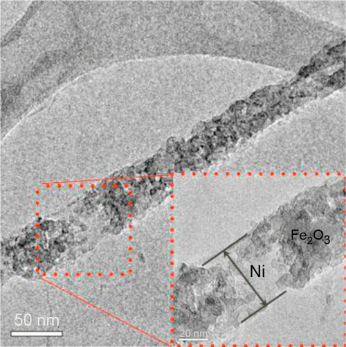
Figure 3.10 shows a TEM image of an M@D nanowire made by our group with this combined technique: A Ni electrodeposited core is wrapped by Fe2O3 nanoparticles produced by a modified sol–gel technique (Pechini, 1967).
The combined techniques allow combining the individual properties of the constituent materials to obtain new, fascinating properties. The resulting composite material has effects derived from the core–shell interaction, such as exchange bias (Nogues and Schuller, 1999), exchange spring magnets (Kneller and Hawig, 1991), and magnetoelectric effects resulting from magnetostriction and piezoelectricity (Eerenstein et al., 2006).
3.6 Multiferroic nanowires
A ferroic material presents spontaneous polarization, magnetic or dipole moment for ferromagnetic or ferroelectric materials, respectively, and strain alignment for a ferroelastic material. Every ferroic behavior can be switched by applying a magnetic, electric, or stress field. These materials by themselves already represent a very well studied class with various technological applications. Multiferroics are an interesting class of materials that are attracting considerable attention because of the interesting fundamental physics involved and their promising practical applications. They combine two or more ferroic properties (Figure 3.11) and can be divided into single phase or multiphase.

3.6.1 Single-phase multiferroic synthesis
Bulk multiferroic properties are rare in nature. For instance, in a ferroelectric crystal, the long-range order exchange required for the electric and the magnetic properties is usually induced by opposed situations with respect to the symmetry of the constituents (Schmid, 2008). However, in structures formed by strongly coupled spin sub-arrays, a strong spin frustration gives rise to complex temperature spin reorganizations. In these situations, the inversion symmetry is broken and makes ferroelectricity possible in the magnetic material. Recently, in manganite rare earths (see Kimura et al., 2003, for RMnO3 and Hur et al., 2004, for RMn2O5 families where R is a rare earth element), a reasonable coupling between ferroic properties is observed. There are other materials that present ferromagnetic and ferroelectric order at the same phase (Hill, 2000; Hill and Filippetti, 2002).
One great example of a room temperature single-phase magnetoelectric material is bismuth ferrite (BiFeO3). This material has an ABO3-type perovskite structure, where the A site has a 12-fold oxygen coordination while the B site has an octahedral oxygen coordination. Although in bulk state this material presents spontaneous ferroelectricity (TC = 1100 K) and antiferromagnetism (TN = 663 K) at room temperature, it can be found presenting a small ferromagnetism in nanoscale (< 62 nm). That happens because BiFeO3 has a g-type antiferromagnetism with a helical ordering of the magnetic moments with approximately 62 nm of cycle. If this helical ordering is interrupted, a small ferromagnetism effect can be viewed (de Oliveira and Pirota, 2013).
However, these single-phase multiferroics are not very attractive for technological applications in the short term because any of the existing materials combine large and robust electric and magnetic polarizations at room temperature (Spaldin and Fiebig, 2005; Spaldin et al., 2010).
The importance of the so-called single-phase multiferroic nanowires lies in how low dimensionality affects the relation between the ferroic properties (Morozovska et al., 2011). For instance, a ferroelectric nanowire would lead to very interesting applications in electronics, the sensor industry, or spintronics via control of the electric behavior by a magnetic field. The need for high-quality single crystals restricts the synthesis of single-phase nanostructures (Chen et al., 2007). They are usually formed by a direct synthesis reaction, usually solvo-thermal processes (Sun et al., 2014; Hu et al., 2008).
3.6.2 Multiphase multiferroic synthesis
The difficulties associated with the coexistence of ferromagnetism and ferroelectricity at the same phase have been solved with the manufacture of two-phase multiferroics in which the ferroelectric and ferromagnetic are different phases. In a general view, such materials can be obtained in different shapes and structures: (1) ferromagnetic nanoparticles by a chemical route embedded in a ferroelectric matrix as in Figure 3.12a, (2) thin film ferromagnetic/ferroelectric multilayers (Figure 3.12b), or (3) ferromagnetic nanowires inside a ferroelectric matrix (Figure 3.12c). In these cases, the coupled effect arises from interface effects between the elastic components of the ferromagnetic and ferroelectric phases. An electric field causes strain in the ferroelectric phase, and this strain is transferred to the ferromagnetic phase, causing magnetization. Thus, the magnetoelectric effect will be greater if we increase the coupling between the interfaces. Larger surface areas with a large magnetostrictive or piezoelectric response are desired in these materials. Employing the combined techniques described in Section 3.5, it is possible to fabricate composite multiferroic nanowires using AAO as a template in core@shell morphology.

3.7 Conclusions
In conclusion, the controlled fabrication of multifunctional single- or multiphase nanowires can play an important role in the design of smart nanodevices. In this chapter, we focus on the fabrication methods based on filling anodic aluminum oxide by electrodeposition or sol–gel techniques. An insight of using the combined techniques was also given, creating the opportunity to fabricate multiphase nanowires with desirable properties. As a perspective, in the case of nanowires or nanotubes fabricated using the anodic aluminum oxide template, it will be very important to develop reproducible methods of single nanowire separation. That can allow for handling of isolated nanowires, which is a very important factor, both for technological applications and for the study of fundamental material properties.