
Spin Hall torque–driven chiral domain walls in magnetic heterostructures
J. Torrejon1,2; M. Hayashi1 1 National Institute for Materials Science, Tsukuba, Japan
2 Unité Mixte de Physique CNRS/Thales, Palaiseau, France
Abstract
The motion of magnetic domain walls in ultrathin magnetic heterostructures driven by current via the spin Hall torque is described in this chapter. We show results from perpendicularly magnetized CoFeB/MgO heterostructures with various heavy metal underlayers. The domain wall moves along or against the current flow, depending on the underlayer material. The direction in which the domain wall moves is associated with the chirality of the domain wall spiral formed in these heterostructures. A one-dimensional model is used to describe the experimental results and extract parameters such as the Dzyaloshinskii–Moriya exchange constant, which is responsible for the formation of the domain wall spiral. Fascinating effects arising from the control of interfaces in magnetic heterostructures are described.
Acknowledgements
The authors thank J. Sinha for preparing samples and characterizing films; J. Kim for measuring the spin Hall effective fields; and M. Yamanouchi, S. Takahashi, S. Mitani, S. Maekawa, and H. Ohno for helpful discussions. This work was supported in part by a Grant-in-Aid (25706017) from the Ministry of Education, Culture, Sports, Science and Technology, Japan (MEXT) and the Funding Program for World-Leading Innovative R&D on Science and Technology (FIRST Program) from Japan Society for the Promotion of Science (JSPS).
10.1 Introduction
Spin transfer torque (STT) (Slonczewski, 1996; Berger, 1996) has enabled control of the direction of magnetization in magnetic nanostructures. In magnetic nanowires, STT allows domain walls, which are boundaries between magnetic domains, to be moved along the wire by a current (Tatara and Kohno, 2004; Zhang and Li, 2004; Thiaville et al., 2005; Barnes and Maekawa, 2005). Such current-controlled motion of domain walls is the key technology of the “racetrack memory” (Parkin et al., 2008), a storage-class, nonvolatile memory that may alter the landscape of storage devices. A series of domain walls can indeed be moved in sync with the application of current pulses (Hayashi et al., 2008; Chiba et al., 2010; Kim et al., 2010). Many of the underlying physics of STT-driven domain wall motion have been uncovered (Thomas et al., 2010; Koyama et al., 2011, 2012), and some prototype devices were recently demonstrated (Fukami et al., 2009; Thomas et al., 2011).
The current-driven motion of domain walls via STT can be considered a bulk effect; the effect of layers adjacent to the magnetic layer is negligible in most cases. However, exciting new phenomena are being discovered in perpendicularly magnetized, ultrathin magnetic heterostructures in which the neighboring layers seem to play a significant role in moving domain walls. First, domain walls can be moved along the current flow, opposite to the STT-driven motion of domain walls, in an ultrathin magnetic layer sandwiched between heavy metal layers or between a heavy metal layer and an insulating oxide layer (Kim et al., 2010; Moore et al., 2008; Miron et al., 2011). More recently, it has been reported that domain walls move either along or against the current flow, depending on the material and stacking order of the heterostructures (Haazen et al., 2013; Ryu et al., 2013; Emori et al., 2013; Koyama et al., 2013; Ryu et al., 2014; Torrejon et al., 2014). These results suggest the importance of the interface(s) of the magnetic layer. Thiaville et al. (2012) suggested that domain walls, provided that they are Neel type, can theoretically be driven by spin current generated in a neighboring layer that diffuses and impinges upon the magnetic layer. The spin Hall effect (SHE) can generate spin current that is large enough to alter the magnetization direction of a magnetic layer placed next to the heavy metal layer (Liu et al., 2012; Pai et al., 2012; Yamanouchi et al., 2013). The torque exerted on the magnetic moments by the impinging spin current is typically called the “spin Hall torque” (Liu et al., 2012), which is to be differentiated from conventional STT as spin orbit coupling plays a role in generating the spin current and possibly the torque.
In a typical perpendicularly magnetized wire, the stable domain wall structure is a Bloch wall (Hubert and Schafer, 2001), in which the magnetization of the domain wall is parallel to the domain boundary. If the width of the wire is sufficiently reduced, magnetostatic energy can force the magnetization of the domain wall to point normal to the boundary (i.e., along the wire’s long axis) and form a Neel wall. Such transition in the wall structure has been observed, for example, in perpendicularly magnetized cobalt (Co)/nickel (Ni) multilayers (Koyama et al., 2011). The magnetization direction of the Neel walls in wires with a narrow width is likely to be random. To move series of domain walls in sync using the spin Hall torque, however, the magnetization direction of neighboring domain walls need to alternate, that is, the chirality of the wall needs to be identical for all domain walls within the wire. This is not possible just by reducing the width of the wire. Such chiral domain walls (Heide et al., 2008) can be realized if the Dzyaloshinskii–Moriya interaction (DMI) (Dzyaloshinskii, 1957; Moriya, 1960), an antisymmetric exchange interaction present in bulk crystals with broken inversion symmetry (Grigoriev et al., 2008; Yu et al., 2010) or at surfaces (Bode et al., 2007) and interfaces (Ryu et al., 2013; Emori et al., 2013; Ryu et al., 2014; Torrejon et al., 2014; Fert, 1990; Chen et al., 2013a,b; Hrabec et al., 2014), is introduced into the system. The coexistence of the SHE and the DMI enables motion of multiple domain walls in sync along or against the current flow (Thiaville et al., 2012; Khvalkovskiy et al., 2013).
In this chapter, we describe spin Hall torque–driven chiral domain walls in ultrathin magnetic heterostructures. The modified Landau Lifshitz Gilbert (LLG) equation, which includes both STT and spin Hall torque, is used to derive the one-dimensional (1D) model of a domain wall (Malozemoff and Slonczewski, 1979). The 1D model is used to analyze the dependence of domain wall velocity on the external magnetic field, which allows the Dzyaloshinskii–Moriya (DM) exchange constant of the system to be extracted. Experimental results of current-driven domain wall motion in magnetic heterostructures are shown to compare them with the 1D model.
10.2 The 1D model of domain walls
The LLG equation that includes adiabatic/nonadiabatic STT and spin Hall torque can be written as (Thiaville et al., 2005; Zhang et al., 2002) follows:

where ![]() and
and ![]() represent unit vectors of the magnetic layer’s spatially varying magnetization and the current flow along the wire, respectively; t is time.
represent unit vectors of the magnetic layer’s spatially varying magnetization and the current flow along the wire, respectively; t is time. ![]() represents the adiabatic STT term, where μB and e are the Bohr magnetron and the electron charge (we define e > 0 for convenience), respectively; P and MS are the current spin polarization and saturation magnetization of the magnetic layer, respectively; and J is the current density that flows through the magnetic layer. β is the nonadiabatic STT term, γ is the gyromagnetic ratio, and α is the Gilbert damping constant. E is the total magnetic energy of the system that includes, for example, the demagnetization, anisotropy, exchange, magnetoelastic, and Zeeman energies.
represents the adiabatic STT term, where μB and e are the Bohr magnetron and the electron charge (we define e > 0 for convenience), respectively; P and MS are the current spin polarization and saturation magnetization of the magnetic layer, respectively; and J is the current density that flows through the magnetic layer. β is the nonadiabatic STT term, γ is the gyromagnetic ratio, and α is the Gilbert damping constant. E is the total magnetic energy of the system that includes, for example, the demagnetization, anisotropy, exchange, magnetoelastic, and Zeeman energies. ![]() .
.
In Eq. (10.1), the spin Hall torque is included in the form of an effective magnetic field: aJ and bJ correspond to the damping-like (Slonczewski, 1996; Berger, 1996) and the field-like (Zhang et al., 2002) components of the effective field, respectively. ![]() is an unit vector representing the spin direction of the electrons impinging upon the magnetic layer via the SHE.
is an unit vector representing the spin direction of the electrons impinging upon the magnetic layer via the SHE.
We use the 1D model of a domain wall derived by Malozemoff and Slonczewski (1979)). The definition of the coordinate system is shown in Figure 10.1. The following ansatz is used for the magnetization profile along the wire:


where θ and φ represent the polar and azimuthal angle, respectively, of the magnetization ![]() that depends on position x and time t. q and ψ are the center position and the magnetization angle of the wall, respectively. ψ = 0, π and ψ = π/2, 3π/2 correspond to perfect Neel and Bloch walls, respectively. Δ is the domain wall width parameter; the physical width of the wall is ~ πΔ. We assume ψ is constant within the domain wall and Δ is independent of both time and space. After some algebra, two coupled ordinary differential equations are obtained from Eq. (10.1):
that depends on position x and time t. q and ψ are the center position and the magnetization angle of the wall, respectively. ψ = 0, π and ψ = π/2, 3π/2 correspond to perfect Neel and Bloch walls, respectively. Δ is the domain wall width parameter; the physical width of the wall is ~ πΔ. We assume ψ is constant within the domain wall and Δ is independent of both time and space. After some algebra, two coupled ordinary differential equations are obtained from Eq. (10.1):

HK is the magnetic anisotropy field associated with the domain wall magnetization; it corresponds to the field needed to cause a transition between the Neel and Bloch walls. The effect of a pinning potential is described by the term with ![]() , where σPIN denotes the wall-pinning potential energy density. HZ, HX, and HY correspond to the out-of-plane, in-plane longitudinal (along the current flow direction), and in-plane transverse (transverse to the current flow direction) external fields, respectively. Γ represents the domain pattern; Γ = + 1 for ↑↓ wall and Γ = − 1 for ↓↑ wall. The effect of DMI on the wall magnetization is included (Ryu et al., 2013; Emori et al., 2013; Ryu et al., 2014; Torrejon et al., 2014; Thiaville et al., 2012) as a longitudinal offset field HDM directed along the wire’s long axis.
, where σPIN denotes the wall-pinning potential energy density. HZ, HX, and HY correspond to the out-of-plane, in-plane longitudinal (along the current flow direction), and in-plane transverse (transverse to the current flow direction) external fields, respectively. Γ represents the domain pattern; Γ = + 1 for ↑↓ wall and Γ = − 1 for ↓↑ wall. The effect of DMI on the wall magnetization is included (Ryu et al., 2013; Emori et al., 2013; Ryu et al., 2014; Torrejon et al., 2014; Thiaville et al., 2012) as a longitudinal offset field HDM directed along the wire’s long axis. ![]() , where D is the DM exchange constant.
, where D is the DM exchange constant.
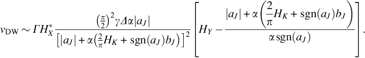
When the spin Hall torque is the dominant driving force in moving domain walls, the steady-state magnetization tilt angle during the current application approaches ψ ~ ± π/2. In the absence of pinning (![]() ), one can then linearize Eqs. (10.3a) and (10.3b) around ψ ~ ± π/2 to obtain the following analytical form of the domain wall velocity (Ryu et al., 2013; Emori et al., 2013, Torrejon et al., 2014):
), one can then linearize Eqs. (10.3a) and (10.3b) around ψ ~ ± π/2 to obtain the following analytical form of the domain wall velocity (Ryu et al., 2013; Emori et al., 2013, Torrejon et al., 2014):

The ± symbol corresponds to the case when ψ approaches ± π/2. From here on, we assume HZ = 0 and β = 0 because the out-of-plane field HZ is set near zero during the measurements of current-driven domain wall velocity, and contribution from the nonadiabatic STT term has been reported recently to be negligible in perpendicular magnetized CoFeB ultrathin films (Fukami et al., 2011). For spin Hall torque–driven domain wall motion, the ± symbol in Eq. (10.4) is given by ![]() . Replacing the ± symbol with
. Replacing the ± symbol with ![]() and substituting HZ = β = 0 in Eq. (10.4) give:
and substituting HZ = β = 0 in Eq. (10.4) give:

Equation (10.5) shows that wall velocity is linear against the in-plane longitudinal field (HX). The intercept between this linear line and the horizontal axis with vDW = 0 gives the compensation field HX*, which contains information on HDM, that is,

If the contribution of STT to the wall motion is absent (i.e., u = 0), then HX* is exactly equal to − HDM. In the heterostructures studied here (X/CoFeB/MgO), however, it turns out that we cannot neglect the influence of u when calculating HDM from HX* because a fraction of current flows into the magnetic layer.
The dependence of the wall velocity against the in-plane transverse field (HY) can be extracted from Eq. (10.4) if HY is small compared with the domain wall anisotropy field HK. Assuming ![]() and substituting HX = 0 in Eq. (10.4) give the following relation between the velocity and HY:
and substituting HX = 0 in Eq. (10.4) give the following relation between the velocity and HY:
Equation (10.7) shows that in the small HY limit, where the wall velocity is linear with HY, the slope of vDW versus HY contains information of HDM via HX*. The magnitude of the slope includes contribution from other parameters (aJ, HK, α, and bJ if any), thus hindering direct evaluation of HDM. The sign of the slope, determined by the product of the wall type and the compensation field, that is, ΓHX*, represents the domain wall chirality if contribution from the STT term is absent (i.e., u = 0): ![]() for left-handed chirality and
for left-handed chirality and ![]() for right-handed chirality.
for right-handed chirality.
In the presence of pinning, the threshold current to move (i.e., depin) a domain wall is obtained by assuming a parabolic pinning potential (Thomas et al., 2006):
where V and q0 are the depth and width of the potential well, respectively, and ϑ(q) is a Heaviside step function. The threshold current is defined as the current needed to shift the equilibrium position of a domain wall out from the well. As described below, the threshold current depends on whether the domain wall is a Neel wall or a Bloch-like wall (Torrejon et al., 2014). To stabilize a Neel wall, the longitudinal offset field HDM needs to overcome the anisotropy field associated with the wall, that is,

If HDM is smaller than HDMNEEL, the wall becomes Bloch-like because the wire width is large enough to stabilize Bloch walls. Reducing the wire width to less than ~100 nm allows, in general, stabilization of Neel walls via a gain in magnetic shape anisotropy (HK then will be negative in Eq. 10.2a and 10.2b). As noted above, one can introduce Neel walls by scaling down the wire width, but the chirality of the domain walls is more or less random, which does not allow in-sync motion of multiple domain walls with the spin Hall torque.
The threshold spin Hall effective fields for depinning the Bloch- and Neel-like walls are expressed as (Torrejon et al., 2014):


where HP is the propagation (depinning) field, which depends on the strength of pinning, that is, ![]() . aJC decreases as the domain wall changes its magnetization direction from a Bloch-like configuration (
. aJC decreases as the domain wall changes its magnetization direction from a Bloch-like configuration (![]() ) to that of a Neel wall. For a perfect Neel wall (
) to that of a Neel wall. For a perfect Neel wall (![]() ), aJC depends only on HP.
), aJC depends only on HP.
10.3 Experimental results
10.3.1 Sample preparation and experimental methods
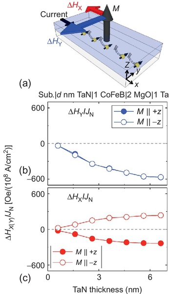
We study magnetic heterostructures consisting of substrate|d X|1 Co20Fe60B20|2 MgO|1 Ta (units in nanometers) using different heavy metal underlayers (X = hafnium [Hf], tantalum [Ta], tantalum nitride [TaN], and tungsten [W]). Films are deposited on thermally oxidized Si(001) substrates (SiO2, 100 nm thick) using magnetron sputtering. The TaN underlayer is formed by reactively sputtering Ta in an argon gas atmosphere mixed with a small amount of nitrogen gas. The atomic composition of TaN is determined by Rutherford backscattering spectroscopy and contains 52 ± 5 at% nitrogen. Films are annealed at 300 °C for 1 h in a vacuum. The thickness of the underlayer X is linearly varied across the substrate to study the thickness dependence of various parameters. The film thickness of underlayer X is calibrated by comparing the resistance (and the anomalous Hall resistance) of a Hall bar patterned on the wedge film with that of a flat film with a constant thickness of X. The magnetic properties of the heterostructures are studied in vibrating sample magnetometry using flat films.
Hall bars and wires are patterned from the films using optical lithography and argon ion etching. A lift-off process is subsequently used to form the electrical contact 10 Ta|100 Au (units in nanometers). The Hall bars used to study current-induced (spin Hall) effective fields are 10 μm wide and 30–60 μm long, whereas the wires for domain wall motion experiments are 5 μm wide and 30 μm long. Details of the device preparation and magnetic, transport, and structural properties of the heterostructures can be found in Torrejon et al. (2014), Kim et al. (2013), Sinha et al. (2013).
10.3.2 Evaluation of the current-induced effective field
Adiabatic harmonic Hall measurements (Kim et al., 2013; Pi et al., 2010; Garello et al., 2013) are used to estimate the current-induced effective field arising from the spin Hall torque. A low-frequency (~ 500 Hz) sinusoidal voltage (amplitude VIN) is applied to the Hall bar and the in phase first (Vω) and the out of phase second (V2ω) harmonic Hall voltages are measured using lock-in amplifiers (Kim et al., 2013). An in-plane field is applied along (HX) or transverse to (HY) the current flow. The field dependence of the harmonic Hall voltages provides information on the longitudinal and transverse effective fields directed along the x and y axes, respectively (Hayashi et al., 2014):

We define ![]() ,
, ![]() , and
, and ![]() , where ΔRP and ΔRA are the planar Hall and the anomalous Hall contributions to the Hall resistance, respectively.
, where ΔRP and ΔRA are the planar Hall and the anomalous Hall contributions to the Hall resistance, respectively.
Both components of the effective field (ΔHX and ΔHY) scale linearly with the amplitude of the sinusoidal voltage (VIN) at low excitation. VIN can be converted to the current density that flows through the underlayer (JN) using the resistance of the wire, the resistivity, and the thickness of the underlayer X and the CoFeB layer. We fit ΔHX(Y) versus JN with a linear function to obtain the effective field per unit current density, ΔHX(Y)/JN.
Results of ΔHX(Y)/JN measured for the TaN underlayer films (substrate|d TaN|1 CoFeB|2 MgO|1 Ta) are shown in Figure 10.1b and c as a function of the TaN underlayer thickness. Solid and open symbols correspond to ΔHX(Y)/JN when the equilibrium magnetization direction is pointing along + z and − z, respectively. As is evident in Figure 10.1, both components of the effective field increase with increasing underlayer thickness. This is consistent with the picture of spin Hall torque, in which the magnitude of the torque scales with the underlayer thickness up to its spin diffusion length (Liu et al., 2011, 2012; Wang and Manchon, 2012; Haney et al., 2013), above which the torque saturates because spin current generated far from the underlayer–magnetic layer interface (a distance larger than the spin diffusion length) loses its spin information before reaching the interface.
Figure 10.1b and c shows that ΔHY/JN is the same regardless of the magnetization direction, whereas ΔHX/JN changes its direction when the magnetization direction is reversed. These results illustrate the correspondence between ΔHX (ΔHY) and aJ (bJ) in Eq. (10.1), that is,

As described after Eq. (10.1), ![]() is the spin direction of the electrons entering the ferromagnetic (FM) layer via the SHE that takes place in the nonmagnetic (NM) underlayer (Figure 10.1a). ΔHX and ΔHY can thus be considered the damping-like and field-like components, respectively. It was recently reported that some components of the current-induced effective field are dependent on the angle between the magnetization and the current (Garello et al., 2013; Pauyac et al., 2013; Qiu et al., 2014). Although these components are reported to be nonnegligible in many heterostructures, here we do not consider these angle-dependent terms when describing domain wall dynamics and thus assume Eq. (10.12) to hold.
is the spin direction of the electrons entering the ferromagnetic (FM) layer via the SHE that takes place in the nonmagnetic (NM) underlayer (Figure 10.1a). ΔHX and ΔHY can thus be considered the damping-like and field-like components, respectively. It was recently reported that some components of the current-induced effective field are dependent on the angle between the magnetization and the current (Garello et al., 2013; Pauyac et al., 2013; Qiu et al., 2014). Although these components are reported to be nonnegligible in many heterostructures, here we do not consider these angle-dependent terms when describing domain wall dynamics and thus assume Eq. (10.12) to hold.
The relative size of the damping-like and field-like terms depends on the materials and thickness of the underlayer and the magnetic layer. For Ta and TaN underlayer films, the field-like term (ΔHY/JN) seems to be two to three times larger than the damping-like term (ΔHX/JN) (Torrejon et al., 2014; Kim et al., 2013). The direction of the damping-like term is consistent with that originally predicted by Slonczewski if one assumes the spins that impinge on the magnetic layer point along the direction dictated by the sign of the spin Hall angle (Liu et al., 2012; Morota et al., 2011). The direction of the field-like term is opposite to that of the incoming spin direction, which is rather counterintuitive. The size and the direction of the field-like term is said to depend on how the electrons reflect and/or transmit the NM–FM interface (Stiles and Zangwill, 2002; Ralph and Stiles, 2008; Kim et al., 2014).
According to Eq. (10.5), the domain wall velocity is proportional to the size of the damping-like term aJ. Thus, based on Eq. (10.12), it is ΔHX/JN that provides the driving force in moving domain walls.
10.3.3 Measurements of domain wall velocity
An optical microscopy image of a typical wire used to evaluate domain wall velocity is shown in Figure 10.2a. The wire width is ~ 5 μm, and we studied the propagation of domain wall(s) over a distance of ~ 30 μm using Kerr microscopy imaging. A pulse generator, which can apply a constant-amplitude voltage pulse, is connected to the wire. Definition of the coordinate axes is the same as that shown in Figure 10.1a. A positive current corresponds to current flow along the + x direction. Exemplary hysteresis loops of the wire for two films with different underlayer materials (Hf and W) are shown in Figure 10.2b. Hysteresis loops are obtained by Kerr microscopy images of the wire captured during an out-of-plane magnetic field sweep (HZ). For all films analyzed here, the switching field is governed by the field needed to nucleate reverse domains and ranges between ~ 100 and ~ 500 Oe.

A domain wall (or domain walls) in the wire is prepared by applying large-amplitude voltage pulses. First, the CoFeB layer is uniformly magnetized by applying a large enough out-of-plane field (HZ). The field is then removed, and a large-amplitude voltage pulse is applied to the wire, which can trigger magnetization reversal (Miron et al., 2010; Shibata et al., 2005). This typically results in nucleation of one or two domain walls within the wire. In some cases, an additional field is applied after the voltage pulse to form an appropriate domain structure. The pulse amplitude needed to trigger magnetization reversal is, in general, larger than that needed to move domain walls; thus this sets the upper limit of the applicable pulse amplitude for studying current-driven domain wall motion.
For studying current-induced domain wall motion, we use ~ 100-ns-long voltage pulses (shorter pulses, 20–50 ns long, are used when the velocity of the wall becomes large). Kerr images are captured before and after the application of the voltage pulse(s) to estimate the distance the wall traveled. Figure 10.2c and d shows such Kerr images for the two films shown in Figure 10.2b. The top images show the initial state with two domain walls in the wire; the bottom images illustrate the magnetic state after application of the voltage pulse. As evident, the two domain walls move in sync with the application of the voltage pulse. The direction in which the walls move depends on the film structure, as discussed below.
Figure 10.2e and f shows successive positions of the two domain walls shown in Figure 10.2c and d, respectively, as voltage pulses are applied to the wire. The cumulated pulse length is shown in the horizontal axis to extract domain wall velocity from this plot. When the driving force is large enough, domain walls can be driven along the wire without pinning. In some circumstances, however, when the pinning is strong or when the driving force is weak, domain walls can get locally pinned. An example of such pinning is shown in Figure 10.2e, where the position of one of the domain walls does not change with the application of voltage pulses (the corresponding cumulated pulse length is ~ 1–2 μs). In this case, after application of a few voltage pulses, the wall depins and restarts its motion along the wire. The average domain wall velocity is estimated by fitting the wall position as a function of cumulated pulse length with a linear function. We exclude cases when the domain wall is locally pinned. The average value of the slope of the solid lines in Figures 10.2e and f gives the domain wall velocity.
Figure 10.3 shows the dependence of domain wall velocity on the current density JN flowing through the NM underlayer for four different film structures. Positive velocity means the domain wall moves along the + x direction. The threshold current needed to trigger the wall motion depends on the film structure (we do not consider creep motion here). According to Eq. (10.10a and 10.10b), domain walls can be moved if the spin Hall effective field aJ exceeds aJC, which depends on the wall structure (Neel-like or Bloch-like) and the domain wall propagation field HP. HP is studied using Kerr images and is defined as the average minimum out-of-plane field needed to move a domain wall along the wire. HP is listed together in each panel in Figure 10.3. The threshold effective field aJC can be calculated using the threshold current density JNC obtained from Figure 10.3 and the effective field per unit JN from Figure 10.1. For example, for a 6.6-nm-thick TaN underlayer film, JNC ~ 0.3 × 10⁸ A/cm2 from Figure 10.3c and ![]() from Figure 10.1c; thus
from Figure 10.1c; thus ![]() ~ 70 Oe (we assume Eq. 10.12 holds here). This is larger than the propagation field (HP ~ 30 Oe), indicating that the domain wall is not a perfect Neel wall. Using Eq. (10.10a), these values give
~ 70 Oe (we assume Eq. 10.12 holds here). This is larger than the propagation field (HP ~ 30 Oe), indicating that the domain wall is not a perfect Neel wall. Using Eq. (10.10a), these values give ![]() , which corresponds to the direction cosine of the magnetization angle with respect to the wire’s long axis (here, along the x-axis).
, which corresponds to the direction cosine of the magnetization angle with respect to the wire’s long axis (here, along the x-axis).

10.3.4 Determination of magnetic chirality
Figure 10.3 shows that the domain wall moves with the current flow for TaN and W underlayer films, whereas it moves against the current flow for the Hf and Ta underlayer films. The direction in which a domain wall moves is determined by the sign of the spin Hall angle and the wall chirality (Ryu et al., 2013; Emori et al., 2013; Ryu et al., 2014; Torrejon et al., 2014; Thiaville et al., 2012), that is, the DM exchange constant. The effective field measurements (e.g., Figure 10.1) can, in general, provide the sign of the spin Hall angle. We find the same sign of the spin Hall angle for all underlayer materials used here (Hf, Ta, TaN, and W) (Torrejon et al., 2014). Note that estimating the size of the spin Hall angle from such measurements is difficult because the size of the effective field depends on the product of the spin Hall angle and the spin mixing conductance of the NM–FM interface (Kim et al., 2014). As shown below, here it is the DM exchange constant that differs depending on the underlayer material; this constant consequently changes the direction in which a domain wall moves.
The in-plane field dependence of the domain wall velocity for the TaN underlayer film is shown in Figure 10.4. The velocity scales linearly with the in-plane field in this field range. For the longitudinal field (HX) sweep, the slope of this linear relationship changes its sign when the current direction is reversed or if the wall type is changed between ↑↓ and ↓↑ walls. By contrast, the slope is the same for ↑↓ and ↓↑ walls, as well as for the positive and negative currents, for the transverse field (HY) sweep. This trend agrees with the 1D model: According to Eqs. (10.5) and (10.7), the sign of the slope of vDW versus HX and vDW versus HY is given by ΓaJ and ΓHX*, respectively (Γ is 1 for the ↑↓ wall and − 1 for the ↓↑ wall). Because aJ depends on the current direction, the sign of the slope for vDW versus HX depends on the wall type and the direction of current flow. The slope of vDW versus HY does not change its sign with the wall type because HX* also depends on Γ via HDM (see Eqs. 10.6 and 10.7). The negative slope of vDW versus HY in Figure 10.4a and b thus indicates that the domain walls are right-handed for this film (TaN underlayer). The longitudinal compensation field HX* can be determined from the plots shown in Figure 10.4c and d.

Figure 10.5 shows the longitudinal field dependence of the wall velocity for three different underlayer films. The sign of the compensation field HX* is opposite for the Hf, Ta and the TaN, W underlayer films (see Figure 10.4c and d for HX* of the TaN underlayer films), which is in agreement with the direction in which domain walls move with current, as shown in Figure 10.3 (the thickness of the underlayer is slightly different in Figures 10.3–10.5). Equation (10.6) shows that HX* is constant regardless of the pulse amplitude (or JN) if the contribution from the STT term is small (u ~ 0). This applies for the Hf and W underlayer films. However, HX* changes appreciably when JN is varied for the Ta underlayer films.

To extract the DM exchange constant properly using Eq. (10.6), the adiabatic spin torque term u and the domain wall width parameter Δ need to be determined. First, the current density (J) that flows into the CoFeB layer needs to be substituted in the expression of u. J is calculated using the thickness and resistivity of each layer: ρCoFeB = 160, ρHf = 199, ρTa = 189, ρTaN = 375, and ρW = 124 μΩ cm (Torrejon et al., 2014). The saturation magnetization depends on the material and the thickness of the underlayer (Sinha et al., 2013); for simplicity, here we assume MS ~ 1500 emu/cm3, which is close to that of bulk Co20Fe60B20. The current spin polarization of the CoFeB layer has been reported to be ~ 0.7 in a similar system (Fukami et al., 2011); we use this value as a median and use the error bars to show the range of the DM exchange constant when P is varied from 0 to 1. The domain wall width parameter is inversely proportional to the effective magnetic anisotropy energy KEFF of the film, that is, ![]() , where A is the exchange stiffness constant. KEFF is determined from the magnetization hysteresis loops (Torrejon et al., 2014), and we use A ~ 3.1 erg/cm3 estimated from a different study reported previously (Yamanouchi et al., 2011).
, where A is the exchange stiffness constant. KEFF is determined from the magnetization hysteresis loops (Torrejon et al., 2014), and we use A ~ 3.1 erg/cm3 estimated from a different study reported previously (Yamanouchi et al., 2011).
In Figure 10.6 we show the compensation field HX* as a function of the underlayer thickness for four film structures. The background color indicates the direction in which a domain wall moves when current is applied. We fit the dependence of HX* on the underlayer thickness using Eq. (10.6); the change in KEFF with the underlayer thickness is taken into account for the fitting. This fitting assumes that the DM exchange constant does not depend on the thickness of the underlayer, which may not be the case, because the thickness can influence the state of the interface both structurally and electronically. The fitted values of the DM exchange constant for all film structures studied are summarized in Figure 10.6e. As evidenced, the DM exchange constant D changes as the underlayer material is varied. D is negative for the Hf underlayer and is nearly zero for Ta. It increases when nitrogen is added to Ta to form TaN, and D takes the largest value here for the W underlayer. These results show that the DM exchange constant can be controlled by the NM–FM interface (Torrejon et al., 2014).

10.4 Concluding remarks
We have described the underlying physics of current-driven domain wall motion in ultrathin magnetic heterostructures. With the introduction of spin Hall torque and a chiral magnetic structure, domain walls can be moved along the wire—either with or against the current flow, depending on the material and stacking order of the magnetic heterostructure. To fully utilize the spin Hall torque and chiral magnetic structure to move domain walls formed in ultrathin magnetic heterostructures, finding a film structure in which the spin Hall torque and the DMI are greatly enhanced is essential. According to the 1D model, Neel walls can be moved with current only when the spin Hall effective field exceeds the wall-pinning field. Thus, to simultaneously achieve thermally stable domain walls and a low threshold current, one needs to find a system in which the spin Hall torque becomes sufficiently large to overcome the large pinning field needed for high thermal stability. This is in contrast to adiabatic STT-driven domain walls, where the threshold current is not related to the pinning field. With the engineering of the film stack and material innovations, however, we hope that this field will grow further and develop viable technologies in the near future.