
Bimagnetic microwires and nanowires
Synthesis and characterization
G. Badini-Confalonieri1; D. Navas2 1 Instituto de Ciencias de Materiales de Madrid, Madrid, Spain
2 Universidade do Porto, Porto, Portugal
Abstract
This chapter reports recent advancements in cylindrical biphase magnetic systems with dimensions ranging from a few nanometers to several tens of microns. We cover the most common processes involved in the preparation of biphase wire systems. Details of appropriate treatments to be used during growth or after preparation are given, with the aim of optimizing the magnetic anisotropy of the systems. The reader is guided through a selection of magnetic materials commonly used in bimagnetic microwires and nanowires. How the properties of the composite fibers are closely linked to the choice of materials is described. A detailed overview of magnetic properties, describing the behavior of individual constituents as well as magnetostatic and magnetoelastic interactions between concentric layers in biphase magnetic systems, is provided. The effect of wire geometry and morphology on magnetic properties is discussed, and guidelines on selecting appropriate materials are given. An overview of proposed technological applications for biphase magnetic wires and nanowires is also presented, and the chapter concludes with a brief summary of the major achievements in the field. A series of suggestions is provided, touching on scientific and technological topics relevant to understanding and addressing the limitations of bimagnetic wires.
9.1 Introduction
This chapter focuses on bimagnetic phase micro- and nanowires. After a brief section introducing this novel family of composite materials and their characteristics, Section 9.2 describes the most common preparation methods. Section 9.3 introduces the core of the discussion, and the reader is guided through a selection of magnetic materials commonly used in bimagnetic microwires and nanowires. How the properties of the composite fibers are closely linked to the choice of materials is shown. A detailed overview of magnetic properties, describing the behavior of individual constituents as well as magnetostatic and magnetoelastic interactions between concentric layers in biphase magnetic systems, is provided. The effect of the micro- and nanowire geometry and morphology on magnetic properties is discussed. The section ends by providing guidelines on selecting appropriate materials to address specific design constraints and application requirements. Biphase magnetic wires have been proposed as potential components in several technological applications, the most promising of which are covered in Section 9.4. Section 9.5 concludes the chapter with a summary of the major achievements in the field, discussing what still needs to be done. A series of suggestions is provided, touching on scientific and technological topics relevant to understanding and addressing the limitations of bimagnetic wires.
Before moving any further in the discussion, we should clarify that this unique family of composite materials is characterized by the presence of at least two different distinct magnetic phases, which are geometrically found along the radius of a multilayer, concentric cylindrical wire or tube. Bimagnetic wires should not, therefore, be confused with other multilayer geometries with only one or no components made of magnetic materials, as described, for instance, in Chapters 7 and 8. Unlike those systems, and despite important similarities, bimagnetic wires have at least two magnetic phases that provide a combination of different magnetic coupling mechanisms that can be engineered into a highly tunable material.
In what might be seen as a somewhat bold move, both micrometric and nanometric composites systems are discussed jointly in the various sections of this chapter. As the reader will be able to appreciate, this allows for interesting comparisons between two families of materials otherwise seldom associated with each other. In any case, we should not forget that composite biphase magnetic microwires and nanowires have a very different history and were developed with techniques and for reasons that have little if nothing in common with each other.
Biphase magnetic microwires were first introduced in a seminal paper by Pirota and coworkers (2004). They made use of glass-coated microwire precursors and a combination of sputtering and electrodeposition techniques. The aim of their work was to obtain multifunctional materials for applications in sensing technologies. This first example of bimagnetic microwires was characterized by having the glass layer act as a nonmagnetic spacer between the two magnetic phases. A few years later, Torrejon and coworkers (2007a) introduced bimagnetic microwires.
Over the last decade, one-dimensional magnetic nanostructures, such as nanowires and nanotubes, have been studied for fundamental and technological interest because of their unique size-dependent properties and the possibility of being functionalized by the controlled modification of their surface properties. However, single-phase nanowires and nanotubes permit the functionalization of only one or two surfaces, respectively. Nanosystems with core/shell architectures, such as bimetallic core/shell nanowires and nanotubes, are being explored, allowing for selective surface modifications.
Although they originated in different ways and for different purposes, both nano- and micro-bimagnetic systems share important advantages:
(1) the ability to combine materials with different chemical and physical properties
(2) the possibility to introduce an inert layer (insulator, diffusion barrier, spacer)
(3) the ability to control each geometric parameter (core radius, shell thickness, and separation between them)
(4) scalability
In an attempt to create a preliminary classification, it is possible to identify two main families of biphase magnetic wires:
(1) Where two magnetic phases are in contact with each other.
(2) Where two magnetic phases are separated by a nonmagnetic spacer
We have described the geometry of bimagnetic cylindrical micro- and nanoelements as consisting of a magnetic wire and a tube that are in contact or separated by a nonmagnetic spacer. The wires are characterized by a length L; the internal wire or magnetic core, characterized by its outer radius (Rint); and the external tube or magnetic shell, characterized by its outer (Rext) and inner radii (rext) (shown in Figure 9.1). If present, a magnetically inert interlayer or nonmagnetic spacer is also characterized by its radii Rint and rext. We will see that the magnetic properties of a multilayer cylindrical wire can be tuned by controlling the dimensions of each component, such as length and radius. Depending on the separation between both magnetic phases, the magnetic coupling could be also controlled. Two kinds of magnetic behaviors are described in this chapter: (1) Bimagnetic structures in which the magnetic phases are in contact have magnetic properties that behave as single system and are mainly controlled by the material occupying the larger fraction of the element volume (Daly et al., 2006). (2) In micro- and nanoelements in which the magnetic phases are separated by a nonmagnetic layer, two magnetic switching events were experimentally observed (Chong et al., 2010) and theoretically confirmed by Sarli and Keskin (2012).

9.2 Preparation methods and choice of materials
Two main processing routes are used in the preparation of multilayer concentric wires: the “center-to-surface” route and the “surface-to-center” route.
9.2.1 Center to surface: an approach for biphase microwires
“Center to surface” refers to those methods where a precursor cylindrical fiber is used as substrate base, on top of which one or more layers are grown. This is typically the case for microwires systems in which the metallic central fiber is often obtained by a metallurgical route. In a second stage, the metallic fibers are coated using chemical or physical deposition methods or a combination of both. A more detailed description of these methods has been provided, for instance, in Chapters 7 and 8. In this chapter, because of their relevance, we remind readers about microwires prepared using the in-rotating-water quenching technique and the quenching and drawing technique. Both are rapid solidification methods that provide amorphous metallic wires, although with different diameter ranges. The main difference between both methods is that, in the latter, the metallic core is coated with a layer of Pyrex-like glass. This, as we will see in the following sections, has important consequences in defining the type and strength of coupling between the two magnetic phases. In both cases, however, the presence of an amorphous metallic core results in outstanding magnetic behavior as a consequence of the intrinsic atomic disorder (Handrich and Kobe, 1980).
A ferromagnetic nucleus covered by a Pyrex layer is obtained using the quenching and drawing method (Figure 9.2b). The diameter of the nucleus and the thickness of the glass cover a range between 1 and 20 μm. Because of the strong quenching rate (~ 105 K s− 1), the ferromagnetic nucleus typically exhibits amorphous structures conferring soft magnetic properties. Three different families of magnetic alloys with soft behavior, characterized by different values of saturation magnetostriction λs, have been considered: iron (Fe)-based (λs = 10− 5), cobalt (Co)-based (λs = − 10− 6), and CoFe-based alloys with vanishing values of saturation magnetostriction (λs = − 10− 7).

Several attempts were made to obtain microwires with harder magnetic behavior (Wang et al., 1997; Zhukov et al., 2000; Chiriac et al., 2001), making use of CoFeCr, CoNiCu, and CoFeMo alloys. These compositions require treatment at a suitable temperature to promote the crystallization of magnetic phases with strong crystalline anisotropy. Others alloys (FeNdB, FePt, FePtNdB, FePd, and CoSm) also were explored; however, their saturation magnetization significantly decreases after treatment at high temperatures. In this chapter we show, as an example, results of an FePt microwire after suitable thermal treatment: The transition from face-centered cubic (FCC) disorder to a face-centered tetragonal ordered phase hardens its magnetic behavior (Torrejon, 2009; Torrejon et al., 2008a).
Using electroplating, further layers are typically grown on top of the amorphous magnetic wires. When glass-coated microwires are used as substrate, a gold (Au) nanolayer (typically 30 nm thick) is grown, typically by sputtering, on top of the glass surface to serve as an electrode for the subsequent electroplating of the magnetic outer layer (Figure 9.2c–e). To date, two main families of magnetic alloys have been proposed as magnetic outer layers: FeNi (Torrejon et al., 2008a,b; Beach et al., 1996; Garcia et al., 2001) and CoNi (Pirota et al., 2005; Torrejon et al., 2007b), with soft and hard magnetic behavior, respectively. The nominal composition of the alloys is tailored through the current density of the electroplating, whereas the thickness is almost proportional to both time and current density. Other parameters affecting the quality and characteristics of electroplating are the electrolyte temperature (optimal temperature of 40 °C for these alloys) and mechanical stirring (Schlesinger and Paunovic, 2000). In some cases, a circular magnetic field is used during FeNi electroplating to induce helical anisotropy (Butta et al., 2009).
For the purposes of this chapter, we selected a series of representative compositions that allow bimagnetic composites with different combinations of hard and soft magnetic phases to be compared. The compositions reviewed, given in the format of nucleus/coating and indicating the magnetic character, are listed in Table 9.1.
Table 9.1
Composition of the samples considered in this chapter
| Sample (nucleus/coating) | Composition (nucleus/coating) | Magnetic character (nucleus/coating) |
| CoFe/CoNi | Co67.06Fe3.84Ni1.44Si14.47B11.53/Co90Ni10 | Soft/hard |
| FeSiB/CoNi | Fe77.5Si7.5B15/Co90Ni10a | Soft/hard |
| CoFe/FeNi | Co67.06Fe3.84Ni1.44Si14.47B11.53/Fe20Ni80 | Soft/soft |
| FeSiBP/FeNi | Fe76Si9B10P5/Fe20Ni80b | Soft/soft |
| FePt/FeNi | Fe63Pt27Si10/Fe20Ni80c | Hard/soft |
a Pirota et al. (2004), Pirota et al. (2005), Torrejon et al. (2007b), and Badini-Confalonieri et al. (2008).
The geometric characteristics of these systems are summarized in Table 9.2.
Table 9.2
Magnetic nucleus radius (Rn), intermediate glass thickness (tg), and range of magnetic outer shell thickness (tCoNi or tFeNi) for different biphase systems
| Sample (nucleus/coating) | Rn (μm) | tg (μm) | tCoNi/tFeNi (μm) |
| CoFe/CoNi | 8.5 | 12 | 0–20 |
| FeSiB/CoNi | 6 | 9 | 0–20 |
| FeSiBP/FeNi | 7 | 12 | 0–7.5 |
| CoFe/FeNi | 7 | 2.5 | 0–6 |
| FePt/FeNi | 20 | 10 | 0–20 |

The FeNi and CoNi electroplated growth results in an FCC and hexagonal close-packed (HCP) crystalline structure, respectively. On the other hand, FePt alloy exhibits an as-cast disordered FCC phase that transforms into to a face-centered tetragonal ordered phase after 15 min of thermal treatment at 823°K (Torrejon et al., 2008a; Torrejon, 2009). It is important to note that different ionic species result in electroplated phases with different surface topologies, which in turn affect the magnetostatic properties of the outer layer. While FeNi-based alloys grow a smooth front with roughness on the order of few tens of nanometers, CoNi alloys form an interlocked network of flakes like grains. This topography, shown in Figure 9.2d, is very similar to that found in gypsum crystal, also known as desert rose, and presents roughness values on the order of several micrometers.
9.2.2 Surface to center: an approach for biphase nanowires
Surface-to-center techniques represent a valid alternative route to prepare core/shell nanostructures, such as Co/magnetite and magnetite/Co nanowire arrays, using a porous anodized alumina template and a supercritical fluid inclusion phase technique (Daly et al., 2006; Kazakova et al., 2006).
Highly hexagonally ordered anodic alumina templates were prepared by a two-step anodization process (Masuda and Fukuda, 1995; Masuda et al., 1997). Self-assembled nanoporous templates are obtained with parallel pores, lengths ranging from a few nanometers to hundreds of micrometers, pore diameters ranging from ~ 10 to ~ 500 nm, and interpore distances from tens of nanometers to half a micron (Li et al., 1998). Thus templates should define the order of the material, the internanoelement distance, and the diameter of the wires or tubes. In this case, a porous anodic alumina substrate template with a pore diameter of 100 nm and a thickness of 60 μm was used. This method was widely described in previous chapters. Then, Co or magnetite nanotubes were synthesized inside the pores of the template in a 25-mL high-pressure cell. Dicobalt octacarbonyl (the Co precursor) or tri-irondodecacarbonyl (the magnetite precursor) was placed in a stainless steel reservoir and dissolved in supercritical carbon dioxide. A high-pressure pump (Isco Instruments, Lincoln, NE) was used to flow the precursor into the 25-mL high-pressure cell containing the anodic aluminum oxide membranes. Moreover, the cell must be placed in a furnace and simultaneously heated to 673°K and pressurized to 37.5 MPa. The chemical reaction is carried out until the entire precursor had passed over the porous membranes and nanotubes are obtained. Then core nanowires were grown inside the deposited nanotubes within a clean cell using the same procedure.
Transmission electron microscopy images of a free-standing Fe3O4 shell/Co core (Fe3O4/Co) nanowire are shown in Figure 9.3a and b after removing the alumina matrix by dissolving the alumina in a potassium hydroxide solution (6 M at 423°K) and washed with distilled water. The magnetite shell has an average wall thickness of 8 nm, while the Co core has a diameter of 84 nm. Both the magnetite shell and the Co core are clearly polycrystalline in nature; several different lattice planes are visible in both the core and the shell material. The Fe3O4 shell confirms the cubic crystallographic structure of magnetite (shown in Figure 9.3b). While the lattice plane 1 corresponds to (333) and they are separated by 1.6 Å (marked 1 in Figure 9.3b), lattice plane 2 corresponds to (311) and they are separated by 2.5 Å (marked 2 in Figure 9.3b). The lattice planes of the Co core (marked 3 in Figure 9.3b) are separated by 2.1 Å, corresponding to the (002) HCP structure of crystalline Co.

Figure 9.3c and d presents transmission electron microscopy images of an individual Co shell/Fe3O4 core (Co/Fe3O4) nanowire. In this case, the Co shell has an average wall thickness of 5.5 nm, while the magnetite core has a diameter of 90 nm. The Co–magnetite interface is shown in Figure 9.3d. The lattice planes of the (101) HCP structure of the crystalline Co shell (marked 4 in Figure 9.3d) are separated by 1.9 Å. The magnetite core shows polycrystalline grains with well-defined grain boundaries. The lattice planes correspond to (311) cubic magnetite and the planes are separated by 2.5 Å.
Regarding the crystallinity of the Co/Fe3O4 and Fe3O4/Co bimagnetic nanowire arrays, high-angle X-ray diffraction also was performed. The X-ray diffraction peaks were indexed and the phases were identified as the magnetite cubic structure (Joint Committee for Powder Diffraction Studies [JCPDS] card no. 74–0748) and the HCP Co phase (JCPDS card no. 01–1277). Moreover, a small amount of cubic-structured Co is also present in the Co shell, which was confirmed by the EXAFS analysis. In the Co shell, 16% of the material can be attributed to the cubic phase; the rest is attributed to the hexagonal phase.
An alternative route to prepare core/shell nanowires and nanotubes with a large aspect ratio is based on using nanoporous anodic alumina templates in combination with electrodeposition and atomic layer deposition (ALD) techniques (Bachmann et al., 2007). Again, highly hexagonally ordered anodic alumina substrates were used as templates. These porous matrices are usually filled with several metallic materials using electrodeposition (Whitney et al., 1993; Thurn-Albrecht et al., 2000). This technique is a versatile, well-established, and low-cost methodology. Although several kinds of nanowires (Metzger et al., 2000; Sun et al., 2000; Nielsch et al., 2000) and nanotubes (Cao et al., 2006; Tao et al., 2006; Han et al., 2009; Xu et al., 2008; Proenca et al., 2012) have been fabricated, this technique is limited to the growth of metallic materials.
To overcome this limitation, ALD is a promising alternative for the preparation of tubular thin films embedded in an aluminum oxide matrix (Sander et al., 2004). ALD allows conformal coating of the pore walls, supported by its self-limiting nature, to be prepared via chemical vapor deposition. The material deposition of individual layers requires chemical precursors and is based on sequential chemical reactions occurring at the sample’s surface. By repeating the process, thin films and multilayers with uniform surfaces, high conformity to template surface features, high control and accuracy of atomic-level thickness, and high reproducibility can be obtained (Puurunen, 2005).
Therefore, both bimagnetic nanowires (Chong et al., 2010) and nanotubes (Pitzschel et al., 2012) have been studied. The overall approach to the synthesis of magnetic multilayered nanowires, such as SiO2/Fe3O4/SiO2/Ni core nanowires, is shown in Figure 9.4. In this case, the porous anodic alumina template was prepared using a two-step anodization process with highly pure (99.999%) aluminum foils and aqueous solutions with 1 wt% phosphoric acid (H3PO4) at 18 °C and an applied potential of 200 V. Under these conditions, the self-ordered anodic alumina membranes show a hexagonally ordered pore array with an interpore distance of ~ 500 nm, a pore diameter of ~ 150 nm, and an ~ 20-μm length. Pores can be widened by immersing the templates in 5 wt% H3PO4 at 45 °C and result in an etching rate of 2 nm min− 1. The porous substrates can be coated onto the inner pore walls using an ALD reactor (Figure 9.4a) with different materials such as silicon oxide (SiO2) by the reaction of 3-aminopropyltriethoxysilane (heated to 100 °C), water (at 40 °C), and ozone (at room temperature) at a chamber temperature of 180 °C. After chemical dissolution of the aluminum substrate, a long H3PO4 etch is created to ensure complete dissolution of the barrier layer (Figure 9.4b) without risk of pore widening. Then, reactive ion etching is used to remove the SiO2-exposed tips, obtaining a membrane with open pores (Figure 9.4c). Finally, the multilayer nanotube arrays are obtained by depositing the subsequent thin layers using ALD (Figure 9.4d). In this case, an Fe oxide layer was grown by sequential pulses of ferrocene (at 100 °C) and ozone (at room temperature) at a reaction temperature of 230 °C, plus an extra thin layer of SiO2.

Before describing preparation of the nanowire core, we should note that the core diameter can be modified by varying the thicknesses of the ALD shell layers. Once the nanowire shell was obtained, an Au electrode was sputtered onto one side of the sample and nickel (Ni) was electrodeposited galvanostatically (10 mA cm− 2) from an aqueous Watts bath (300 g L− 1 of NiSO4·6H2O, 45 g L− 1 of NiCl2·6H2O, and 45 g L− 1 of H3BO3; Figure 9.4e) (Nielsch et al., 2001; Sellmyer et al., 2001). Also, we should remark that the inner silica tube serves as an electrical insulator. Finally, the Au electrode was chemically removed by KI3, and the Fe2O3 was reduced to Fe3O4 by a thermal treatment at 400 °C for 12 h and in a controlled atmosphere of 5% hydrogen/95% argon (Bachmann et al., 2007) (Figure 9.4f).
Figure 9.5 shows scanning electron microscopy images of the nanotube and nanowire arrays after various fabrication steps. The hexagonal order and diameter homogeneity of the nanotube and nanowire arrays, as well as the complete filling of the pores, was confirmed (Figure 9.5c and d). Isolated tubes and core/shell wires were investigated by transmission electron microscopy (Figure 9.5e–g), revealing that each ALD layer is uniform and smooth.

An SiO2/Fe2O3/SiO2 tube with an external diameter of 170 nm and a layer thicknesses of 5/12/10 nm, respectively, are shown in Figure 9.5e. After filling the tube core with electrodeposited Ni and the Fe2O3 reduction, SiO2/Fe3O4/SiO2/Ni shell/core nanowires were prepared. While Figure 9.5 presents a bimagnetic nanowire with an external diameter of 150 nm, a layer thicknesses of 5 nm (SiO2)/12 nm (Fe3O4)/10 nm (SiO2), and a 95-nm-diameter Ni core, a nanowire with a larger Fe3O4-to-Ni ratio and an external diameter of 130 nm, a layer thicknesses of 5 nm (SiO2)/18 nm (Fe3O4)/25 nm (SiO2), and a 35-nm-diameter Ni core is shown in Figure 9.5g. Controlling the amount of oxides deposited by ALD allows the diameter of the central ferromagnetic wire, the ferromagnetic shell layer, and the magnetostatic interactions between them to be set.
9.3 Magnetic materials and properties
This section guides the reader through a selection of magnetic materials commonly used in bimagnetic microwires and nanowires. How the properties of the composite fibers are closely linked to the choice of materials is shown. A detailed overview of magnetic properties is provided, describing the behavior of individual constituents as well as magnetostatic and magnetoelastic interactions between concentric layers in biphase magnetic systems. This section begins with a review of the properties of microwire systems, and readers will be able to appreciate the similarities between nanowire counterparts.
9.3.1 Static magnetic properties of biphase microwires
When dealing with systems that have two magnetic phases, it is possible to extract information on the behavior of the composite as a whole, as well as to study the contributions of individual elements. For this purpose, establishing measuring protocols in the field domain, the time domain, or both is important. Magnetic microwires are typically studied using a vibrating sample magnetometer and/or by inductive fluxmetric techniques. Useful information is obtained from hysteresis loops at (1) a high field to analyze the biphase character and (2) a low field (with a demagnetized or premagnetized hard phase) to determine magnetic interactions.
Major loops of biphase microwires present a typical behavior of two Barkhausen jumps. In soft/hard systems (Figure 9.6a), a low field jump corresponds to magnetization reversal of the soft phase—CoFe, FeSiB, or FeNi—whereas a wider jump at a higher field denotes the reversal process of the harder phase: CoNi or FePt. In a system of soft CoFe/soft FeNi, both layers reverse magnetization at a similar field range (FeNi presents higher permeability) (El Kammouni et al., 2011), whereas in FeSiBP/FeNi, magnetization at the outer shell reverses first, followed by the single Barkhausen jump of the nucleus (Infante et al., 2010). The fractional section of each layer determines the amplitude of each jump and the coercivity of the biphase system (Pirota et al., 2005; Torrejon et al., 2008b).
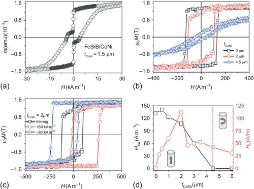
Minor loops, obtained after demagnetizing the hard phase, show practically only the magnetization process of the soft phase. Bistable magnetic behavior, with a single giant Barkhausen jump, is observed FeSiB nuclei with positive magnetostriction for external hard phases with small thicknesses (Figure 9.6b). Magnetization is reversed by a single domain wall being depinned from the closure structure at the end of the wire and its propagation (Varga et al., 2005). The domain structure is composed of a main axial core and a thinner radial outer shell, as defined by the fabrication stresses induced by quenching, drawing, and any glass cover. The relative volume of that axial domain increases with the thickness of the glass cover, producing a stronger longitudinal anisotropy and resulting in a higher remanence Mr and switching field Hsw. The fractional radius Rc/R of the axial core reversed by domain wall propagation is given by (Rc/R)2 = (Mr/Ms) (Vazquez, 2007; Chiriac et al., 1995).
The presence of a CoNi layer tCoNi with increasing thickness induces internal stresses σCoNi. The corresponding magnetoelastic anisotropy deteriorates (progressive reduction of Mr and Hsw) and finally destroys the bistable behavior (see Figure 9.6b and d) with a multidomain structure. According to the sign of magnetostriction λs, σCoNi is tensile axial or compressive transversal (Torrejon et al., 2008b) in character, and its strength (i.e., σCoNi = 400 MPa for tCoNi = 4.5 μm) is estimated by (Aragoneses et al., 1998; Varga et al., 2003):
where Hsw0 is the switching field of the single-phase microwire, γDW is the energy density stored at the domain wall, and α is a geometric factor. Magnetoelastic coupling also was analyzed in the alternative soft/hard CoFe/CoNi biphase system, where magnetostriction of the CoFe nucleus is small and negative (Torrejon et al., 2007b) and its domain structure is characterized by a main circumferential domain but contains an inner axial vortex structure (Torrejon et al., 2011, 2013). In this case, the stresses induced by the external CoNi layer give rise to an effective axial anisotropy that is reflected in a progressive reduction with increasing layer thickness of the circumferential anisotropy field Hk and a parallel increase in susceptibility χ (i.e., Hk = 40 A m− 1 and χ = 11,000 for tCoNi = 11 μm). Such stresses (i.e., σCoNi = 350 MPa for tCoNi = 11 μm) can be quantified by:
where Hk0 is the anisotropy field for the glass-coated, single-phase CoFe microwire.
The presence of an external layer, together with that of an intermediate Pyrex layer, is a source of stresses at the nucleus when the temperature is modified (i.e., reduced). Thermoelastic stresses have been ascribed to the different thermal expansion coefficients of the metallic nucleus (αn = 12 × 10− 6 K− 1) and the insulating glass cover (αg = 3 × 10− 6 K− 1) (Chiriac et al., 1995; Chiriac and Ovari, 1996; Varga et al., 2003). The evolution of magnetic properties with decreasing temperature is mainly determined by the glass layer, whereas the CoNi outer shell only modifies the initial magnetic structure. In CoFe/CoNi (FeSiB/CoNi) biphase systems, an increase in temperature reduces Hk (Hsw), that is, it induces a magnetoelastic axial (circumferential) anisotropy. Therefore, the temperature change plays the same role as that of the CoNi thickness. Thermal stresses can be estimated using the previous expressions, taking into account the temperature dependence of the saturation magnetization Ms(T) and magnetostriction λs (T) (Torrejon, 2009).
Finally, in the case of a hard/soft FePt/FeNi biphase system, the magnetoelastic coupling during electroplating of the soft magnetic phase is nearly negligible. The hard magnetic behavior of the nucleus is governed by the magnetocrystalline anisotropy of the L10 phase. On the other hand, temperature changes affect only the magnetic behavior of the FeNi outer shell, reducing remanence and coercivity and decreasing temperature (Torrejon, 2009; Torrejon et al., 2008a).
Parallel to the magnetoelastic coupling, the magnetostatic interaction between magnetic phases can be relevant (Torrejon et al., 2007b; Badini-Confalonieri et al., 2008). Its origin is found in the uncompensated magnetic charges at the ends of a premagnetized harder phase. They generate a magnetostatic field that adds to the applied field and biases the magnetic state of the soft phase. Figure 9.6c shows the minor hysteresis loops of the FeSiB/CoNi microwire (tCoNi = 2 μm) when the hard phase is demagnetized and premagnetized at ± 80 kA m− 1, respectively. The minor loop is shifted toward a positive (negative) field when the CoNi layer has been magnetically saturated along a positive (negative) orientation; that is, the bias field Hb is antiparallel to the magnetization of the hard phase. Moreover, premagnetized wires show asymmetric magnetization reversal. After positive premagnetization, the magnetization reversal in the lower branch (from a negative to a positive field) takes place fully by domain wall propagation, whereas in the upper branch (from a positive to a negative field), a partial region reverses by rotation followed by domain wall propagation. The opposite behavior occurs after negative premagnetization. This asymmetry can be explained by the stronger inhomogeneity of the bias field in the region close to the uncompensated charges, and it forces such a region to reverse by rotation instead of domain wall propagation (Badini-Confalonieri et al., 2008).
The magnetostatic bias depends greatly on the thickness of the CoNi layer. The evolution of Hb with tCoNi is observed in Figure 9.6d: The bias field increases with the thickness until a critical tCoNi of 2 μm, reaching a maximum value of Hb at 112 A m− 1. The strong reduction of Hb for CoNi layers thicker than the critical value is correlated to a change in the magnetic structure in the FeSiB nucleus, as was previously shown in the magnetoelastic analysis (Figure 9.6b). There, bistability and the single axial domain disappear, leading to a change of magnetization easy axis from an axial to a circumferential direction. The same bias field evolution was observed in the alternative soft/hard CoFeSiB/CoNi biphase system, where a maximum Hb is measured for tCoNi = 8 μm. The bias field was analytically modeled in terms of the geometry of the biphase system as (Escrig et al., 2009):

where RGC = Rn + tg and V is the total volume of the microwire. Calculations predict a strong Hb dependence on the thickness and length L of the hard magnetic outer shell, particularly that it reaches a maximum at a given critical thickness. In the case of a soft/soft FeSiBP/FeNi biphase system, the switching field Hsw of the nucleus can be effectively controlled by the dipolar interaction with the FeNi outer shell through its geometry (thickness and length) (Infante et al., 2010). Finally, in a hard/soft FePt/FeNi biphase system with the opposite magnetic configuration, the magnetostatic field is created by the hard nucleus and the shifted magnetization curves correspond to the softer FeNi outer shell. The bias field decreases strongly with FeNi thickness, as was expected: Thicker FeNi layers are less affected by Hb (Torrejon et al., 2008a).
9.3.2 Dynamic magnetic properties of biphase microwires
The study of dynamic magnetic properties in microwires has been extended to the radio and microwave frequency range for the case of soft/hard (CoFeSiB/CoNi and FeSiB/CoNi) and soft/soft (CoFeSiB/FeNi) biphase configurations. The presence of an intermediate glass layer electrically insulates the internal and external metallic layers, and it allows the alternating current (AC) excitation of the nucleus, whose permeability will be affected by the magnetic interactions between metallic layers. Two phenomena are studied: giant magnetoimpedence (GMI) and ferromagnetic resonance (FMR).
GMI consists of the huge changes in wire impedance under the action of a static field or a stress. Its origin in ultrasoft magnetic systems relates to the variations of the skin effect (Panina and Mohri, 1994; Beach and Berkowitz, 1994; Knobel et al., 2003) observed when a high-frequency current flows along the wire in the presence of a static magnetic field. The penetration depth δ of the skin effect is given by
where, for amorphous materials, the resistivity ρ is relatively high and δ < Rn at the megahertz frequency F range. In a GMI configuration, the AC flows along the nucleus of the biphase wire, inducing an AC circumferential field, exciting the circumferential permeability μ. After the action of a weak static field, permeability is modified and, consequently, the skin effect penetration depth, with the final variation of impedance. The protocol for measuring GMI is the same as for static properties: The low-field GMI of the soft nucleus is measured with the hard magnetic layer in a demagnetized or premagnetized state.
Figure 9.7a illustrates the GMI effect of CoFe/CoNi wires for tCoNi = 6 μm at 50 MHz. We observe typical double-peak behavior, where the maximum impedance is achieved at a static field balancing the circumferential anisotropy field, Hk = 2K/μ0Ms. The magnetostatic bias field Hb shifts GMI curves toward a positive (negative) field after positive (negative) premagnetization, as expected. In addition, the GMI curves show asymmetric behavior as a consequence of nonhomogeneous Hb. So, the peak with lower (higher) intensity is related to the region close to the ends (center) with stronger (weaker) Hb and lower (higher) susceptibility (Torrejon et al., 2009a). The evolution of the bias field with the frequency for selected tCoNi is plotted in Figure 9.7b. First, for small thicknesses, Hb is nearly constant in the whole frequency range, and it shows a progressive increase with tCoNi. The data obtained using the GMI technique are in agreement with static measurements when tCoNi is < 8 μm. We should note that the GMI technique analyzes only the surface impedance, whereas magnetometric inductive techniques account for the whole magnetic volume of the samples. Concerning the influence of magnetolastic coupling, the demagnetized GMI curves exhibit a transition from a double to single peak as tCoNi increases (data not shown). It denotes a change in the anisotropy from circular to axial (Torrejon et al., 2009a). Finally, in the case of FeSiB/CoNi biphase wires, the GMI effect of FeSiB is very small. Its transition from single-peak (axial anisotropy) to double-peak (circular anisotropy) GMI observed with increasing tCoNi agrees with data in Figure 9.6b.

The engineering microwave properties of amorphous, glass-coated microwires have been previously reported in both axial and circumferential radio frequency field configurations (Menard and Yelon, 2000; Reynet et al., 2002; Lofland et al., 2002; Makhnovskiy and Panina, 2003; Kraus et al., 2011). Here we focus on the circular configuration (circumferential radial-dependent AC field generated by an AC flowing along the ferromagnetic nucleus). The impedance has been measured using microstrip and transmission coaxial line techniques connected to a vector network analyzer (Torrejon et al., 2009a,b; Menard et al., 1997).
Nonmagnetostrictive CoFe microwires present a single electromagnetic absorption at frequencies between 1 and 6 GHz for a saturating magnetic field in the range of kiloamperes per meter. In turn, bistable FeSiB microwires show FMR at higher frequencies (6–12 GHz) and even in the absence of any applied static field, an effect that is labeled natural FMR, in which the role of the saturating field is played by the strong axial anisotropy field (Torrejon et al., 2009b). The presence of a second hard phase modifies the microwave frequency response.
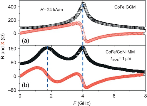
Figure 9.8 illustrates the impedance spectra (real and imaginary components) for single-phase CoFe glass coated microwire (GCM) and biphase CoFe/CoNi multilayer microwire (MM) with tCoNi = 1 μm at a constant field of 24 kA m− 1. The main resonance, FMR1, at around 4 GHz, corresponds to the excitation of CoFe. The CoNi layer introduces a second peak at a lower frequency, FMR2 (1.75 GHz). The impedance spectra of FeSiB/CoNi MM in Figure 9.9a show a third absorption peak, labeled in principle as FMR3, at an intermediate frequency between FMR1 and FMR2.

To get deeper information about the origin of the absorption phenomena, experimental data have been fitted to the Kittel relation (Kittel, 1996) for the macrospin approach. Note that the model for a cylinder is not valid because of the presence of the strong skin effect, and we have to consider a hollow cylinder tube as the model for a more suitable thin plate (Kraus et al., 2011). In the particular case of Ms ![]() (H + Hk), the evolution of FMR frequency Fr with static applied field H is given by:
(H + Hk), the evolution of FMR frequency Fr with static applied field H is given by:
where γ is the gyromagnetic factor. From the fitting, we can evaluate the saturation magnetization Ms and the anisotropy field Hk. Figure 9.9b depicts the square absorption frequencies as a function of H for a single-phase FeSiB microwire and FeSiB/CoNi biphase microwires. FMR, FMR1, and FMR3 curves show similar Ms values (i.e., slope) close to the expected value obtained from static vibrating sample magnetometry data (μ0Ms = 1.55 T). A remarkable difference is found when extrapolating the two curves at F = 0. FMR and FMR1 curves show a positive extrapolated field, Hk = 3 kA m− 1 (i.e., axial anisotropy), whereas for FMR3, the extrapolated negative value Hk = − 18 kA m− 1 denotes a circumferential anisotropy. The FMR2 curve presents an anomalous small slope for which the Kittel relationship is no longer valid (El Kammouni et al., 2011; Torrejon et al., 2010). The origin of FMR2 absorption in CoFe/CoNi and FeSiB/CoNi has been correlated to a capacitance effect between the metallic layers, which depends on the Pyrex thickness. CoNi absorption is not well defined because of the lack of magnetic saturation caused by its harder character. Multipeak electromagnetic absorption was observed in soft/soft CoFeSiB/FeNi MM, where FMR3 was ascribed to the excitation of the FeNi outer shell (Torrejon et al., 2010; El Kammouni and Vazquez, 2013).
9.3.3 Magnetic properties of biphase nanowires
The magnetic properties of Fe3O4/Co and Co/Fe3O4 bimagnetic nanowires with diameter of 100 nm were investigated (Figure 9.10) and compared with the properties of single-phase Co and magnetite nanowires with the same geometry (Kazakova et al., 2006) when the external magnetic field was applied along the nanowires long axis. While the Fe3O4/Co sample shows a Fe3O4 shell thickness of about 8 nm and 84-nm Co core diameter, for the Co/Fe3O4 wire the Co shell thickness is around 2.5 nm and the Fe3O4 core diameter is 95 nm.

The room-temperature hysteresis curve of an Fe3O4 (8 nm)/Co (84 nm) nanowire array is described by a large coercive field of ≈ 39 mT and a saturation magnetization Ms of about 915 kA m− 1, which is lower than the Ms bulk value of 1124 kA m− 1 that is expected for a bulk material of the same composition and assuming the Ms of Co is 1400 kA m− 1 and of Fe3O4 is 480 kA m− 1. Moreover, the saturated state is achieved in an applied field of 0.2 T. At T = 1.8 K, the coercive field is increased to ≈ 58 mT and the magnetization saturation is 1145 kA m− 1, in agreement with bulk values (1133 kA m− 1) at low temperatures. The Co (2.5 nm)/Fe3O4 (95 nm) nanowire array, however, shows a narrower hysteresis loop with a coercivity field of ≈ 0.5 mT and a lower saturation magnetization of 520 kA m− 1 (bulk Ms value = 572 kA m− 1). This behavior can be associated with a magnetically soft system, and the saturated state is achieved in an applied field of 1 T. The large magnetic field required for complete saturation of the Co (2.5 nm)/Fe3O4 (95 nm) sample is related to the formation of a Co oxide layer at the alumina template–Co and Co–Fe3O4 interfaces (van der Zaag et al., 1995, 1996). At low temperatures, the shape of the hysteresis curve changes dramatically, which is reflected in an enormous increase in the coercive field (228 mT). The increase of the measured magnetic moment and the absence of saturation in high fields confirm the presence of a paramagnetic impurity in the alumina template membrane.
To clarify the role of different materials, magnetic properties of bimagnetic nanowires were compared with those of single-phased Co and magnetite nanowires with a diameter of 100 nm and a length of about 60 nm (Figure 9.11). Co nanowires show similar behavior at room and low temperatures. While the coercivity field of the Co nanowire array increases from 36 mT at room temperature to 106 mT at 1.8 K, the magnetization saturation value is increased from 1090 to 1270 kA m− 1. However, the behavior of magnetite nanowires is significantly different at room and low temperatures. At T = 300 K, a low coercivity field of 0.7 mT and a magnetization saturation value of 400 kA m− 1 were obtained. As temperature decreases, the hysteresis curve becomes much broader, with a coercive field of 37 mT, and the magnetization saturation increases to 460 kA m− 1. Thus, while Co nanowires can be characterized as magnetically hard in the whole temperature range, the magnetite nanowires possess very soft magnetic properties at room temperature but become significantly harder in the low-temperature regime. Therefore, it was confirmed that the magnetic properties of bimagnetic nanowires are mainly determined by the material occupying the larger fraction of the volume or the nanowire core.

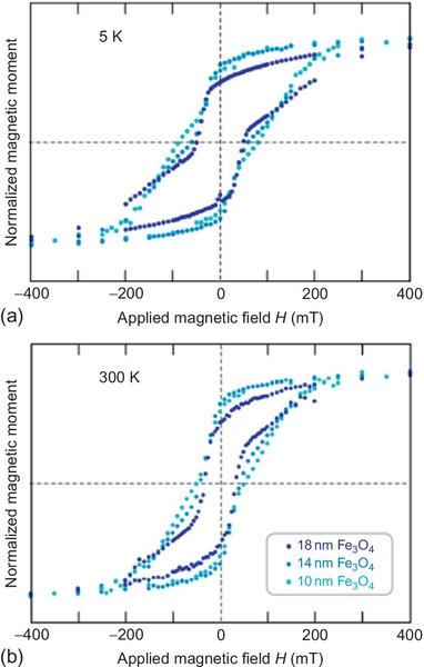
On the other hand, Figure 9.12 shows the hysteresis loops of a core/shell system (5 nm SiO2/18 nm Fe3O4/25 nm SiO2/Ni core) at 5 K (a) and 300 K (b) when the external magnetic field was applied parallel to the nanowire long axis. For comparison, a Ni array with a 54-nm diameter and an Fe3O4 nanotube array have also been studied and were used as references.

In agreement with the literature (Bachmann et al., 2007; Nielsch et al., 2001), while the Fe3O4 nanotube array shows a smooth hysteresis loop with a gradual transition from a positive to a negative response and with a very large coercive field (150 mT at 5 K), the Ni nanowire array with a 54-nm diameter presents a highly square hysteresis loop with an abrupt magnetization reversal step at moderate fields (56 mT at 5 K). However, the core/shell behavior combines the distinctive features of both references, the Fe3O4 nanotube and the Ni nanowire arrays. This fact is clearly observed in the corresponding susceptibility curves (Figure 9.13a), where the hysteresis loops were derivate. In this kind of analysis, the magnetization reversal appears as peaks that are centered in the switching field. Therefore, the Ni cores revert near 42 mT, whereas the outer iron oxide shells gradually switch between approximately + 300 and − 300 mT. Similar behavior has been observed for two magnetic thin films with a nonmagnetic spacer (Platt et al., 2000). Although both magnetic phases seemed to interact weakly, small differences between the peaks of the core/shell and reference samples (Figure 9.13) confirm a nonzero interaction between cores and shells.

To understand the role of the magnetostatic interaction between cores and shells, stray fields have been estimated. Although research has confirmed that the stray fields between a core and its surrounding shell are negligible (< 1 mT) (Escrig et al., 2009), the overall stray field generated by the array of nanomagnets is significant. The average values of the demagnetization fields of a nanomagnet array at saturation can be considered a film with dilute magnetic material, and it can be represented by:
where Ms is the saturation magnetization of Fe3O4 and Ni (![]() ), and
), and ![]() and fNi are the volume fraction of each material in the nonmagnetic matrix. Then, and assuming
and fNi are the volume fraction of each material in the nonmagnetic matrix. Then, and assuming ![]() from the sample geometry, an average stray field on the order of 20–30 mT was obtained near the surface of the array (Landeros et al., 2009). Therefore, when either the core or the shell reverses, the presence of a domain boundary generates locally very intense stray fields with a few tens of megatons in magnitude, which is close to the shifts in switching fields observed when Ni wires are added into the magnetic shell.
from the sample geometry, an average stray field on the order of 20–30 mT was obtained near the surface of the array (Landeros et al., 2009). Therefore, when either the core or the shell reverses, the presence of a domain boundary generates locally very intense stray fields with a few tens of megatons in magnitude, which is close to the shifts in switching fields observed when Ni wires are added into the magnetic shell.
Moreover, several samples with different Fe3O4 thicknesses and a constant spacer layer thickness were studied; they show systematic changes in hysteresis loops (Figure 9.14) and susceptibility curves (Figure 9.13b). Switching fields move to larger values with increasing shell thicknesses. Then, the broad peak shifts to higher fields, from 126 ± 8 to 137 ± 11 mT and eventually 168 ± 21 mT as the Fe3O4 thickness increases from 10 to 18 nm. The sharp peak moves from 23.8 ± 2.2 to 28.2 ± 0.8 mT and finally to 42.4 ± 0.6 mT when the Ni core diameter decreases from 70 to 54 nm. Both observations are in agreement with the literature dealing with arrays of simple tubes (reversing their magnetization via the vortex mode) (Escrig et al., 2008) and of simple Ni wires, respectively (Nielsch et al., 2001).
The magnetization reversal processes suggested from the data analysis are shown at the top of Figure 9.13. In a large positive applied field, both the core and the shell are saturated along the field’s direction. When the magnetic field is reduced to zero, no changes in the Ni core are observed, but the Fe3O4 signal is reduced and the magnetic moments of the shells start curling near their extremities (Holz and Kronmüller, 1968). Then, at a small negative applied field, the Ni core suddenly switches completely. Finally, a large negative field causes the shell to gradually reverse its magnetization.
The magnetization and susceptibility of a cylindrical core/shell spin-1 Ising nanowire was theoretically investigated within the effective field theory, with correlations for both ferromagnetic and antiferromagnetic exchange interactions between the shell and the core (Sarli and Keskin, 2012). The magnetization reversal processes were observed as peaks in the susceptibility versus switching field curve defining the coercivity fields of the nanowire system. In agreement with the results observed for Fe3O4/SiO2/Ni bimagnetic nanowires (Chong et al., 2010), it was confirmed that bimagnetic nanowire systems exhibit two distinct susceptibility peaks and two successive phase transitions; either both of them are second-order transitions or one is a second-order transition and the other is a first-order transition for a small exchange interaction.
Moreover, interesting magnetic properties such as dipolar magnetic bias have been studied in biphase magnetic nanowires in which the internal and external layers can be close enough to interact via a strong dipolar coupling (Escrig et al., 2007). This property was previously reported in microwires (Escrig et al., 2009; Vazquez et al., 2007), and it was investigated by means of numerical simulations in nanowires (Allende et al., 2009). In this analysis, 500-nm-long bimagnetic nanowires, formed by a Ni core with a 30-nm diameter, a nonmagnetic interlayer of 15 nm, and a Co shell with layer thickness ranging from 0 to 300 nm, have been studied by scaling relations in combination with Monte Carlo simulations (Allende et al., 2009).
Then, when the external magnetic field was applied along the wire long axis of Ni wires covered by an external Co shell of varying width, the calculated hysteresis loops showed that the loops were shifted toward positive fields because of the dipolar interaction between both magnetic phases; this shift increases with the shell thickness (Figure 9.15). Moreover, an interesting feature observed in the calculated hysteresis loops is that they are asymmetric. To understand this behavior, the reversal processes have been studied. For these geometric dimensions, the reversal has been considered to occur via domain wall propagation (Wernsdorfer et al., 1996), and variations in the reversal process should be related to the nonhomogeneity of the magnetic field (Hshell) acting on the core wire for the external layer magnetized along the long wire axis. Therefore, it was determined that away from the wire tips the field is weaker and practically parallel to the cylinder axis, and its magnitude decreases toward the center of the wire. Also, the field gradient seems to depend on shell thickness, becoming less important as this thickness increases. Then, nanowires with a 10-nm-thick Co shell show almost symmetrical hysteresis loops (Figure 9.15a). In this configuration, the Hshell profile indicates a narrow region at the wire tips, with a size comparable to the domain wall width, with a strong magnetostatic field where the domain walls nucleate. Along the rest of the wire the field is weak and varies little. Therefore, in addition to the shift, the bimagnetic nanowire hysteresis loop behaves as that of isolated nanowires (Wernsdorfer et al., 1996). For a 90-nm-thick Co shell, a different situation was observed: After nucleation and launching, the domain walls are accelerated by a strong field. Then the walls reach the central part, where the magnetostatic field is weaker; they slow down, leading to a change in the slope of the left hysteresis branch (Figure 9.15c). The right hysteresis branch, however, shows a different mechanism because now the magnetostatic field enhances the stability of the magnetized wire. In this case, the walls nucleated at the tips are almost static, while additional walls appear at the central part of the wire, where the magnetostatic field is weaker, and propagate toward the tips. Finally, in the 300-nm-thick Co shell, the field is very intense along the tube and almost homogeneous, except for at the tips. In the inversion from positive to negative saturation, the nucleation process and propagation are very fast. The propagation speed was so fast that the nucleation of the second wall, at the other tip, was not observed in this simulation. In the other branch, the field is almost homogeneous and so intense that the nucleation of the walls in the central part is not possible. As a result, this branch of the hysteresis loop is initially rounded, corresponding to the walls moving against stronger fields, and then they are accelerated by the weaker central field. In conclusion, the dipolar field of the external shell layer originates a bias of the hysteresis loop. The inhomogeneity of this field is responsible for the existence of different reversal processes, which lead to nonsymmetrical hysteresis loops. The behavior of these systems is the result of a competition between the strength of the magnetostatic field due to the external shell and its inhomogeneity. Bimagnetic nanowires allow control of several aspects of magnetic behavior, such as the coercivity, switching processes, and bias effects.

9.4 Applications
This section provides an overview of proposed technological applications for biphase magnetic microwires and nanowires.
9.4.1 Applications of biphase magnetic microwires
During the past 30 years, amorphous microwires have been proposed for several technological applications. Because of their unique combination of properties, biphase magnetic microwires open the way to novel functionalities. In this section, we consider two particular developments as examples, namely, a multifunctional sensor and the improvement of existing elements for orthogonal flux-gate sensors.
A multifunctional sensor was obtained using a biphase CoFe/CoNi MM as the sensing element (Vazquez et al., 2006; Torrejon et al., 2007a). The magnetization of the nearly nonhysteretic soft, magnetic CoFe nucleus is very sensitive to small changes in environmental conditions (i.e., temperature, stress, and magnetic field), where the hard CoNi outer shell plays a complementary role to control its magnetic state. Two operational principles are used: (1) the modified small-angle magnetization rotation (MSAMR) technique (temperature and mechanical stress sensor) (Torrejon et al., 2007c) and (2) the asymmetric magnetoimpedance (AMI) (position and magnetic field sensor). The MSAMR is based on the classical small-angle magnetization rotation method introduced by Narita et al. (1980), which was used for many years to quantify almost vanishing λs values. This method required the axial magnetic saturation of a soft core (i.e., by means of a direct current axial field created by a solenoid), and the application of a small-amplitude AC transverse field (i.e., by means of Helmholtz coils or a current flowing along the sample) (Hernando et al., 1986) to induce small-amplitude oscillations of the magnetization. The amplitude of oscillations depends on the static field or mechanical stress to be sensed, typically by a pickup coil wound around the wire.
In the MSAMR method, the saturating field and stress are provided by the stray field and the stress introduced by the hard phase (Vazquez et al., 2006; Torrejon et al., 2007a). A schematic of the process is shown in Figure 9.16a.

The MM sensor element was connected to an LCR analyzer that procured the flow of an AC through the wire nucleus and at the same time gave an impedance reading of the nucleus itself. Figure 9.16b depicts the temperature-induced change in fractional inductance of the core. This variation is magnetoelastically induced by the stresses arising from the different thermal expansion coefficient of the multilayer microwire. A noticeable increase (6.3%/°C) of the inductance value around the temperature of the human body is observed. The temperature sensor shows a fast and efficient response with a time constant of τ = 0.7 s in at ΔT = 25 °C (Vazquez et al., 2006; Torrejon et al., 2007a,b,c, 2009c). In addition, the sensor can be used simultaneously to sense tensile (Figure 9.16c) and torsional (Figure 9.16d) stresses (Zhukov et al., 1996).
A second method makes use of the AMI effect, where single-phase CoFe GCM presents symmetric double-peak behavior, whereas in asymmetric GMI, we make use of the large variation in impedance with the static magnetic field, as well as its linear dependence, facilitates the signal recording. Several alternatives have been proposed to achieve AMI: (1) using a pulse bias circuit (Mohri et al., 2002), (2) applying a direct current (Kraus et al., 2003), and (3) analyzing the diagonal component of impedance using a pickup coil wound around the microwire (Sandacci et al., 2004). These methods require additional electronics and sometimes a higher power consumption and sometimes cause difficulties in the positioning of the magnet. In the case of biphase microwires, the stray field of the CoNi outer shell produces a straight such AMI response around zero static field (Figure 9.16e) without additional electronic components (Torrejon et al., 2009a). The optimum result, with a change in linear impedance around 50%, was found in a CoFe/CoNi MM when tCoNi = 4 μm.
Functional sensors based on biphase systems have been tested for biomedical applications for monitoring cardiorespiratory activity and rapid eye movement phases (Pfutzner et al., 2006; Kaniusas et al., 2006). In general, sensor devices based in biphase microwires present advantages such as high sensitivity, quick response time, simplified and robust technology, reduced fabrication cost, easy integration in miniaturized devices, and a multifunctional character.
We now consider the use of biphase microwires in fluxgate sensors. Fluxgates based on microwires are very sensitive magnetic field sensors and are widely used. They are usually classified as parallel and orthogonal, depending on the relative orientation of the excitation and sensed fields. While many applications are based on parallel fluxgates because of their good properties, orthogonal fluxgates have been recently rediscovered thanks to the use of magnetic microwires as the core instead of bulk cylinders (Sasada, 2002). The sensing element consists of a magnetic microwire where an AC flows along the wire, generating the circumferential excitation field that avoids the need for any excitation coil (a pickup coil is still necessary to measure the variation of the longitudinal field). Glass-coated bimetallic microwires offer an additional advantage. They are composed of a Pyrex-coated copper microwire core covered by a relatively thin, soft magnetic material layer, typically permalloy (Py), as in previous biphase microwires. The copper core carries the AC (the thin Pyrex coating insulates both metallic layers) that results in the circular magnetic saturation of Py.
The microwire can work in coil-less fluxgate mode (i.e., without the need for any coil) if the magnetic outer layer exhibits helical anisotropy. In that case, under an applied longitudinal field to be sensed, circular magnetization changes are caused by the helical anisotropy. There, an output signal is received from the ends of the external permalloy (Py) layer; the signal is proportional to changes in the circular magnetization of the wire. Such helical anisotropy can be achieved by mechanically twisting the wire. However, that method shows a sensor stability drawback. An alternative technique has been proposed whereby an intrinsic helical anisotropy is induced during Py electroplating by (1) a helical magnetic field (superposition of a longitudinal field generated by a Helmholtz coil and a circumferential field produced by a direct current flowing through the copper core) (Figure 9.17a; Butta et al., 2010; Vazquez et al., 2009), and (2) a torque applied to the multilayer microwire that is afterward relieved, thereby keeping a helical backstress (Figure 9.17b) (Infante, 2010; Butta et al., 2013). In both cases, a second harmonic signal evolves linearly with the magnetic field in a range that can be tuned by Py electroplating parameters.

9.4.2 Application of biphase magnetic nanowires
The synthesis of biphase nanowires opens the possibility of fabricating ferromagnetic systems in which the internal core and the external shell are close enough to interact via a strong dipolar coupling. Apart from new magnetic states of the cylindrical particle as a whole, which can be used for particular applications, new magnetic properties are expected, such as a dipolar magnetic bias responsible for the GMI behavior of amorphous microwires (Sinnecker et al., 2005). In particular, there is great interest in the development of a spin-valve-like system because its hysteresis loop has shown the potential applicability to sense magnetic fields in magnetic recording systems (Escrig et al., 2007). Finally, research has shown how core/shell wire systems can be used for data storage applications. They can achieve four different remnant states, or metastable states, in zero applied magnetic field when the core and shell are saturated in the same or opposite directions, allowing the storage of two bits of information per core/shell wire (Chong et al., 2010).
9.5 Final conclusions and future perspective
Now we give a few final words to conclude. We can describe bimagnetic phase wires, both micrometric and nanometric in size, as composite systems displaying emerging properties and in which complex unique magnetic behavior can be observed. There is remarkably similarity behavior between specific systems that differ both in size by orders of magnitudes as well as in composition, indicating that common mechanisms that are geometrically controlled are at play both in nanometric as well as in amorphous micrometric systems.
From a technological point of view, several prototypes have been proposed, proving the potential for these families of materials in different advanced applications. Despite recent studies and advancements, there is still scope for deepening the understanding of these composite systems. Again, from a technological perspective, embedding nanostructures within existing technologies often represents a considerable challenge. It should also be noted that bimagnetic phase wires are extremely sensitive to minimal variations in their geometry and preparation methods. Microwire-based systems are, moreover, characterized by the intrinsic disordered structure of the amorphous cylindrical precursor. To be of use in mass-produced technological applications, as has been suggested, it is important to define a complete set of parameters and treatments aimed to stabilize and homogenize the properties.
The dynamic properties of these systems still require more understanding, in particular in systems of nanowire arrays when both the scale as well as the presence of collective interactions create several difficulties when retrieving empirical evidence or interpreting results. The presence of different magnetic phases with distinct ferromagnetic resonance frequencies is clearly advantageous when designing multiband frequency filters. However, further work is required to reduce the bandwidth of the resonance peak, which, at the moment, can often span several tens of megahertz.
In conclusion, over several years of research, the scientific community has achieved a good level of understanding of biphase magnetic wire systems. We are now witnessing an exciting moment in which, going one step further, translation of this knowledge to industrial applications, with all the challenges involved, is occurring.