
Recent developments in the manipulation of magnetic domain walls in CoFeB–MgO wires for applications to high-density nonvolatile memories
D. Ravelosona1; L. Herrera Diez1; W. Zhao1; M. Klaui2; B. Ockert3; R. Mantovan4; A. Lamperti4; L. Baldi5; V. Jacques6; L. Vila7; R. Cowburn8; J.P. Adam1; G. Agnus1; I. Barisik1; C. Burrowes1; C. Chappert1; T. Devolder1; A. Digiacomo1,4; S. Eimer1; K. Garcia1; F. Garcia Sanchez1; M. El Hadri1; J.-V. Kim1; W. Lin1; N. Vernier1; Y. Zhang1; G. Tallarida4; M. Fanciulli4; L. Lazzarini4; L. Nasi4; M. Marianni4; T. Hingant6; J.-P. Tetienne6 1 Université Paris Sud-CNRS, Orsay, France
2 Johannes Gutenberg-Universität Mainz, Mainz, Germany
3 Singulus Technology AG, Kahl am Main, Germany
4 IMM-CNR, Agrate Brianza (MB), Italy
5 Micron Semiconductor Italia S.r.l., Agrate Brianza (MB), Italy
6 Universite' ́Paris-Sud, Orsay, France
7 CEA and Universite' ́Grenoble Alpes, Grenoble, France
8 University of Cambridge, Cambridge, UK
Abstract
The recent discovery that magnetic domain walls can be moved under a small current without any magnetic field opens a perspective for a paradigm shift in mass storage design. However, several fundamental questions must be answered before the technology can be considered feasible. This review covers the current understanding of domain wall (DW) propagation in CoFeB–MgO structures with perpendicular magnetic anisotropy. These films exhibit a very low density of pinning centers and can be integrated in Magnetic Tunnel Junctions, making them very promising for manipulating multiple domain walls in ultra-high-density spintronic devices. Several important issues are addressed: the physics of magnetic field, current and electric field driven domain wall motion, the characterization of the pinning potential on the nanoscale, the demonstration of artificial storing pinning sites, and the evaluation of domain wall propagation for logic and memory design integrated into complementary metal-oxide semiconductor (CMOS) technology.
11.1 Introduction
Fast, high-capacity, low form factor and low power nonvolatile memories are crucial for information and communication technologies (ICT) (http://www.itrs.net/Links/2013ITRS/Home2013.htm). They are already an important part of all electronic systems, representing a growing market segment, and should increase their importance in the future en route to the “Storage everywhere” society. Today’s market is dominated by flash NAND memory and hard disks, and although both currently undergo tremendous increases in performance (with somewhat complementary strengths), they also face severe limitations on the midterm horizon:
• Several physical factors will limit the scalability of flash cells beyond 20 nm. And if today’s progress is oriented towards multibit/cell structures or 3-D stacking of memory layers, such implementations might reduce reliability, speed, and yield.
• Hard disk storage has had increases comparable to that of a CMOS CPU in density and data transfer rates, but the access time was only slightly reduced from 50 to ~ 5 ms, with no hope to reduce it well beyond this latter value within the “rotating disk” paradigm. The hard disk is already the slowest component of a PC, being replaced by solid-state disks in the most stringent cases.
• Volatile DRAM continues to be the fastest memory in today’s market. However, scalability below 20 nm is the main issue. As feature sizes decrease, the DRAM’s capacitor element is not able to maintain the necessary charge. DRAM manufacturers are now trying to remedy this issue by creating three-dimensional charge-holding elements or using other novel circuitry to create a larger capacitor.
The embedded memory market has evolved into a renewed search for a universal memory technology, which is now defined as a single RAM type. For instance, among others, concepts such as resistive RAM, phase change RAM, ferroelectric RAM, or spin-transfer torque RAM technology combines nonvolatility, excellent scalability, endurance with lower power, and fast read and write. However, like other disruptive embedded memory technologies, it faces many challenges and even possible drawbacks beyond 20 nm. A trade-off must often be found between design and technology because the optimized technology for a memory cell is not the same as that for embedded logic devices. Also, solutions are required to address issues of development complexity, manufacturing cost, and yield improvement.
New successful approaches have to be able to provide higher density portable memory systems at low cost. A novel solution can emerge from approaches based on magnetic domain walls (DWs) that can be considered as nano-objects (width 1–100 nm), separating regions of opposite magnetization in thin ferromagnetic films (Slonczewski, 1972; Malozemoff and Slonczewski, 1979; Hubert and Schafer, 2001; Ferré, 2002; Ravelosona, 2009). Indeed, one crucial breakthrough in spin electronics has been achieved regarding the possibility to move magnetic domain walls in magnetic tracks using the sole action of an electrical current (the so-called spin transfer effect) instead of a conventional magnetic field (Chappert et al., 2007; Brataas et al., 2012). This important discovery has opened a perspective for a paradigm shift in mass storage design and has led to the proposition by IBM of the simple stand-alone “storage track memory” concept, also called “magnetic shift register,” compatible with the back end flow of standard CMOS operations (Parkin, 2004; Parkin et al., 2008; Hayashi et al., 2008). It proposes a very good compromise between capacity and speed that can overcome the limitations faced by NAND flash. The “storage track memory” stores information in domain wall (DW) sequences, moving in the same direction under current in patterned magnetic tracks in front of fixed read and write heads. The most general principle is displayed in Figure 11.1, from which many variants can be developed such as closed loop tracks, heads below or above the track, and straight or bent tracks that could pave the way from a 2-D to a 3-D design with the associated higher storage density. The concept reproduces the data sector organization of a hard disk, well adapted to mass data storage, but has no moving mechanical parts, preserving the fast access time of a CMOS circuit. Storage tracks could be arranged in a tightly packed array of stripes at minimum pitch, with memory bit size limited on one side by lithography and on the other by the recording density of the magnetic medium, while programming and reading heads need to be present only every 64–128 bits or more, depending on the application targeted.

Single magnetic domains and domain walls can be thermally stable in nanostructures having nanoscale dimensions, and the wall widths can scale with the wire width, making the racetrack memory concept magnetically scalable down to the ultimate node. Also, the “current control” appears promising in terms of fast stand-alone memories as it seems compatible with standard CMOS operations. As the value of the current density J is the important physical parameter to move a DW, a smaller value of the required current I is expected when decreasing the technological node F, that is, I = J * F * t where t is the magnetic film thickness (~ 10 nm). Providing the current density is not too high < 107 A/cm2, this makes these “current control” class devices scalable to the ultimate node with typical current I of a few microamphere for technology nodes F < 45 nm. Furthermore, due to recent advances in spin electronics, the racetrack memories concept provides superior performance with respect to flash and HDD such as faster read and write access times, lower power dissipation (read and write energy of ~ 1 pJ/bit), infinite endurance, and higher reliability even for a conservative 2-D geometry not considering the striking potential when using a 3-D architecture, which is a unique opportunity for long-term development of an even higher storage density racetrack.
However, several scientific and technological breakthroughs remain to be achieved before the racetrack memory concept can be taken to an industrial environment: new materials with a low density and distribution of structural defects, low current densities below 1011 A/m2, demonstration of functionalities in sub-20 nm wires, demonstration of density prospects in a mass storage device, integration into CMOS technology, and manufacturability issues. In this context, the use of materials with perpendicular magnetic anisotropy (PMA) is actively pursued. The large anisotropy values in such materials yield narrow domain walls (~ 1–30 nm typically) (Hubert and Schafer, 2001; Ferré, 2002; Ravelosona, 2009), making them good candidates for extending the scaling of spintronic devices down to the nanometer scale. However, in ultrathin film or multilayers exhibiting PMA, these narrow domain walls (DWs) interact very strongly with a distribution of random nanoscale inhomogeneties present in thin films, which are detrimental for future applications (Ferré, 2002; Ravelosona, 2009). Recent studies have shown that CoFeB alloys, an amorphous soft magnetic material that crystallizes into the bcc structure after annealing at temperatures around 300 °C, exhibits strong PMA when grown as an ultrathin film (< 1.5 nm) on a Ta buffer layer and capped with MgO (Ikeda et al., 2010). This material combination has been widely studied in magnetic tunnel junctions with in-plane anisotropy because of the high spin polarization of CoFeB and the relatively large tunneling magnetoresistance (TMR) ratios of CoFeB/MgO/CoFeB structures (Stuart, 2004). The presence of a fully crystallized bcc phase leads to a low density of structural defects with respect to conventional fcc textured 3-D ferromagnetic metals with PMA such as Co/Ni, Co/Pd, or Co/Pt multilayers, which is favorable for DW motion.
In this chapter, we present an overview of the results obtained in our groups on the manipulation of DW motion in CoFeB–MgO structures with perpendicular anisotropy. After presenting their structural and magnetic properties as well as the process to fabricate nanowires (Section 11.2), we describe the results on field driven domain wall motion (Section 11.3), and we give insight into the pinning potential (Section 11.4). We then demonstrate the proof of concept of manipulating DW dynamics using a polarized current (Section 11.5) and an electric field (Section 11.6). The possibility to control domain wall pinning using artificial storing potential will be examined in Section 11.7. Finally possible circuits architecture based on racetrack memory device integration into CMOS technology will be described in Section 11.8.
11.2 Structural and magnetic properties of CoFeB–MgO structures
This section is dedicated to the description of the structural and magnetic properties of high-quality Ta–CoFeB(1 nm)–MgO(2 nm) ultrathin films grown by an advanced sputtering technique. The development of nanowires with a low density of patterning-induced defects is also described.
11.2.1 Deposition technique
For applications to memories based on domain wall motion in nanowires, the deposition plays a key role. Superior thickness uniformity, precise thin-film controllability, and smooth interfaces are necessary. The CoFeB and MgO layer thicknesses are typically in the range of 1 nm, and to control this with ± 0.01 nm accuracy is necessary to get repeatable and uniform properties.
These challenges cannot be met with traditional physical vapor deposition (PVD) systems using simple parallel target-substrate configuration. Currently, two types of specially designed PVD cluster systems are capable of meeting these demanding requirements: linear dynamic deposition (LDD) design without fast substrate rotation, and noncoaxial oblique substrate-target design with fast substrate rotation.
A film deposited by a PVD cathode (usually DC magnetron sputtering) on a fixed wafer substrate underneath will not have a particularly good thickness uniformity because the erosion profile of the cathode will be imaged into the substrate. There are some techniques for overcoming this nonuniformity issue, such as rotating the noncoaxial wafer underneath the cathode or rotating an off-centered system of permanent magnets behind the target. For the case of the very thin films under discussion here, this method requires several tens of rotations to obtain the desired uniformity effect. Because the deposition time for the very thin film is short (e.g., a few seconds for about 1 nm and below), a very high rotation speed of the wafer is needed with implications of drawbacks: compatibility with ultrahigh-vacuum chamber, long-term mechanical reliability, and particle generation. The alternative is to reduce the deposition rate, which could increase the impurity level by the residual gas in the deposition chamber.
The LDD technology moves wafers linearly underneath the target and can achieve high thickness uniformity in large-scale deposition (up to 300 mm) without rotating the wafer. This LDD technology also bears other superior deposition characteristics such as good coating efficiency by using short target-wafer distance (TWD, ~ 2 in.), precise thickness controllability (by precisely varying pass speed of the wafer underneath the target) better than 0.01 nm, and mechanical reliability because no high-speed wafer rotation and movement are involved and no mechanical shutter is needed. In addition a large range for the deposition rates is available without compromising the uniformities and the repeatability of the extreme thin films.
In this study, we have used a TIMARIS system from Singulus (Figure 11.2) involving a Multi Target Module, an Etch Module, a Transport Module and two Load locks. In the MultiTarget Modules the LDD technology is used. The targets are assembled on a drum, and by rotating the drum the material can be selected. This results in a short dwell time between the depositions. This is very important because the magnetic anisotropy of these films are controlled by the interfaces.

The target to substrate distance is smaller compared to the mean free path of ad-atoms in low deposition pressure, which promotes high surface mobility for ad-atoms at the substrate surface, resulting in smooth surface morphology. The metallic layers such as CoFeB or Ta are typically deposited by DC-Magnetron sputtering, whereas the insulting layers such as MgO are deposited by RF-Magnetron sputtering.
11.2.2 Structural properties
We have focused on the investigation of the structural properties of Si/SiO2/Ta(5 nm)/Co40Fe40B20(1 nm)/MgO(2 nm)/Ta(5 nm) stacks deposited by the TIMARIS system described in Section 11.2.1 (Mantovan et al., 2013; Lamperti et al., 2013). The films have been deposited at room temperature and annealed at 300 °C for 2 h to crystallize the as deposited amorphous CoFeB layer into a bcc phase. Given the small thickness of the magnetic layer (1 nm), we have demonstrated a very high structural quality of the CoFeB–MgO materials compatible with the racetrack memory prerequisites. In particular as deposited and annealed stacks and multilayers were studied in terms of structural, chemical, and magnetic characterization by a wide range of techniques such as X-Ray Reflectivity (XRR), X-Ray Diffraction (XRD), Time of Flight Secondary Ion Mass Spectrometry (ToF-SIMS), Transmission Electron Microscopy (TEM), Vibrating Sample Magnetometry (VSM), Magneto Optical Kerr Effect (MOKE), and Ferromagnetic Resonance (FMR).
From XRR measurements, typical CoFeB/MgO interface width is 0.21 and 0.20 nm before and after annealing, respectively. This result is of much importance in the view of the implementation of these structures for the fabrication of the nanowire and its integration with reading and writing heads because it underlines the capability of the adopted TIMARIS system to finely control the growth process and to produce a stack with high thermal stability upon annealing. From XRD, contributions from Ta (110) and CoFeB (200) are detected, and peak intensity increases on annealing, indicating that the annealing process promotes the crystallization. Specifically, by following peaks evolution, a partial rearrangement of Ta crystalline structure at Ta/CoFeB or MgO/Ta interface could play a role, in competition with MgO crystalline structure, in determining the CoFeB crystallinity and ultimately its magnetic properties. This is a possible indication that Ta (which has a bcc crystalline structure) may also favor the bcc crystallization of MgO, thus accommodating the crystallization of the thin CoFeB layer as bcc structure.
To get additional information on the possible effects of the annealing treatment, samples have been also analyzed by ToF-SIMSdepth profiling, as shown in Figure 11.3a as a function of the sputtering time. A thin Ta2O5 layer at the surface is evident, but limited to a fraction of the deposited Ta top layer, thus preserving the Ta/MgO interface. MgO and CoFeB layers can be distinctively identified, with well-marked interfaces. However, a possible, minor presence of Co, Fe, and B in the MgO layer cannot be completely ruled out, as evidenced by the increase in the Co, Fe, and B intensity beginning at the Ta/MgO interface. More interestingly, B shape profile is seen to change on annealing: the B intensity is seen to clearly decrease in CoFeB layer and concomitantly increase in bottom Ta layer upon annealing. This change in intensity indicates that B content reduces on annealing in CoFeB, possibly affecting its original composition. Further, the Ta bottom layer acts as a sink layer to B, which diffuses in it, without affecting MgO layer composition (as also indicated by the prefect superimposition of B profile of as-grown and annealed sample inside MgO). As a consequence, the change in B content can effectively affect (that is reduce), CoFeB crystallization temperature.

 ) and annealed (•). Arrows evidence bottom Ta layer acting as B sink layer upon annealing. (b) HRTEM cross-section images of an annealed Si/SiO2//Ta(5)/Co40Fe40B20(5)/MgO(5)/Ta(5) structure. Adapted from Mantovan et al. (2013) and Lamperti et al. (2013).
Finally, high-resolution (HR)-TEM analysis was performed on as-deposited and annealed (300 °C, 2 h) Si/SiO2//Ta(5)/CoFeB(1)/MgO(2)/Ta(5) and Si/SiO2//Ta(5)/CoFeB(5)/MgO(5)/Ta(5) stacks. Figure 11.3b shows an HRTEM cross-section image for a Si/SiO2//Ta(5)/CoFeB(5)/MgO(5)/Ta(5) stack. Thickness of each layer is precisely close to the nominal values, interfaces appear to be smooth and layer crystallinity is clearly evidenced. In particular, also considering the diffractograms, crystalline phase is identified, and a d-spacing d(002) = 0.21 nm is obtained in both MgO and CoFeB, indicating that both layers share a common d-spacing, whereas for Ta a d-spacing d(110) = 0.233 nm can be measured. Such values indicate the existence of crystalline relations among the layers in the stack. These results are consistent with the findings from XRR and XRD analysis, evidencing the very smooth character of defect-free crystalline interfaces.
11.2.3 Magnetic properties
We have investigated the magnetic properties of three different CoFeB compositions, namely Co20Fe60B20, Co40Fe40B20 and Co60Fe20B20 (Burrowes et al., 2013). The full structure consists of Si/SiO2/Ta(5 nm)/CoFeB(1 nm)/MgO(2 nm)/Ta(5 nm). As described in Section 11.2.2, these samples have been annealed at 300 °C for 2 h to promote the full crystallization of the ultrathin CoFeB layer. The samples with compositions Co20Fe60B20 and Co40Fe40B20 exhibit perpendicular anisotropy in the as-deposited (amorphous) state, which can be seen in the hysteresis loops measured by Kerr microscopy (Figure 11.4a and b). For samples with composition Co60Fe20B20 (Figure 11.4c and d), the as-deposited state is magnetized in the film plane, and PMA emerges only following annealing at 300 °C (Figure 11.4d). As suggested by XRD, thermal annealing promotes an increase of CoFeB–MgO interface anisotropy through the crystallization of the CoFeB layer into the bcc phase. This effect is illustrated by the hysteresis loops measured in perpendicular fields becoming sharper after annealing with a slight increase of the coercive field Hc.

The magnetic properties of the CoFeB–MgO samples have been characterized with a number of different methods and are summarized in Table 11.1 (Burrowes et al., 2013; Devolder et al., 2013). The saturation magnetization MS is observed to increase on thermal annealing, which is related to the B diffusion in the bottom Ta layer during the annealing process (Munaka et al., 2005) as evidenced by ToF-SIMS (see Section 11.2.2). Also, due to the crystalline structure of the MgO–CoFeB and Ta–CoFeB interfaces, the effective anisotropy fields, H0, increase after annealing. The Gilbert damping parameter α as measured by VNA-FMR (Devolder, 2013) shows very low value with respect to conventional films with PMA such as Co/Pt, Co/Pd, Co/Ni or FePt. Finally, the DW width ranges from 10 to 30 nm for amorphous and crystalline structures, respectively. Such narrow 1D DWs are very rigid interfaces in comparison with larger 2-D–3-D Neel DWs in soft materials. On the one hand, this makes such 1-D propagating nano-objects in patterned ultrathin magnetic films a very good model system to study the physics of a 1-D elastic interface moving in a confined 2-D geometry. On the other hand, narrow domain walls (DWs) interact very strongly with random nanoscale inhomogeneities present in the thin magnetic films, giving rise to random pinning events. The pinning effect introduces not only stochastic DW dynamics involving thermal activation over energy barrier but also deformation of the DW profile as we will show in part 2.
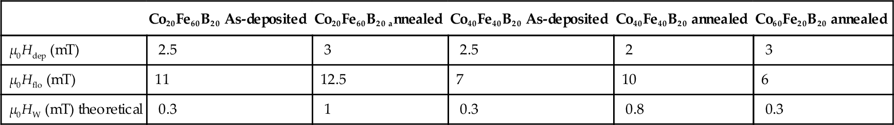
Table 11.1
Magnetic parameters for CoFeB–MgO films with PMA
| Co20Fe60B20 As-deposited | Co20Fe60B20 annealed | Co40Fe40B20 As-deposited | Co40Fe40B20 annealed | Co60Fe20B20 annealed | |
| μ0Hk,eff (mT) | 45 | 430 | 107 | 397 | 82 |
| μ0Ms (T) | 1.38 | 1.41 | 1.26 | 1.38 | 1.1 |
| α | 0.014 | 0.015 | 0.012 | 0.013 | 0.016 |
| Δ | 30.2 | 9.7 | 21 | 10.7 | 27.7 |

Adapted from Burrowes et al. (2013).
![]() is the effective anisotropy field, Ms the saturation magnetization, α is the damping parameter, and Δ is the DW width.
is the effective anisotropy field, Ms the saturation magnetization, α is the damping parameter, and Δ is the DW width. ![]() has been determined from hysteresis loop measurements at varying field angles (relative to the film plane) and corroborated by vector network analyzer ferromagnetic resonance (VNA-FMR) measurements. The DW width has been estimated following the expression for 1D Bloch walls
has been determined from hysteresis loop measurements at varying field angles (relative to the film plane) and corroborated by vector network analyzer ferromagnetic resonance (VNA-FMR) measurements. The DW width has been estimated following the expression for 1D Bloch walls ![]() , where A is the exchange constant and Keff is the effective anisotropy given by Keff = K1 – 2πMs2 where K1 is the first-order interface anisotropy constant. The exchange stiffness of CoFeB films was estimated from a stoichiometry averaging of Co and Fe constant.
, where A is the exchange constant and Keff is the effective anisotropy given by Keff = K1 – 2πMs2 where K1 is the first-order interface anisotropy constant. The exchange stiffness of CoFeB films was estimated from a stoichiometry averaging of Co and Fe constant.
11.2.4 Nanofabrication of magnetic wires
In the following some basic principles of the nanofabrication process of nanowires by lithography techniques are presented. They rely mainly on the development efforts produced by the CMOS technology over the last 50 years. Those have led to a dramatic miniaturization of the devices sizes and a huge increase of complexity as well as of functionality and numbers of transistors numbers per chip. The spintronics research activity has strongly benefited from this expertise developed for CMOS devices, which has led today to the development of STT-RAM memories. The development of racetrack memory devices based on magnetic nanowires is less mature. One important goal for this technology to compete with FLASH memories is the manipulation of DWs in sub-20 nm tracks. As narrow DWs are very sensitive to nanoscale inhomogeneities, this involves a minimization of extrinsic defects introduced by the nanotechnology process such as, for instance, edge roughness or etching damages. In the following, we describe the process for developing nanowires down to 20 nm in size with a low density of patterning-induced defects.
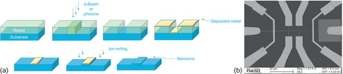
Figure 11.5 shows a typical lithography process based either on optical or e-beam lithography. First a resist is deposited on the magnetic structures by spin coating. Two categories of resist can be used, either positive or negative, depending on the fact that there will remain (negative) or not (positive) after development of the insolated area. The resist is then exposed to UV light (optical lithography) through a mask or directly to electron beam (e-beam lithography) that alters the exposed areas. The following step makes use of a chemical solvent that reveals the exposed areas. This process induces open area in the resist similar to a stencil mask. At this point there are two possibilities. First a metal is deposited to fill the open area and serves, for instance, as an electrical contact or a hard mask for subsequent etching (see Figure 11.6). Second, the material is etched through the nonprotected area of the resist mask. In both cases, the remaining resist is removed by using a chemical process. In the case where a metal is deposited through the mask, the removal of the resist is called a liftoff process.

To etch the magnetic materials, reactive ion etching (RIE) is the method of choice for an industrial process, as it avoids material redeposition (including on the side of the mask) and allows a material etching selectivity to ensure a good control to stop the etching on a specific layer. A plasma of reactive species (argon, oxygen, fluorine or chlorine gases) is formed that will react with the material etched by an incoming flux of atoms like Ar. The main idea is to (1) find a gases mixture that will make volatile the etched species and (2) passivate the edges of the material being etched to obtain a very vertical profile and a high-aspect ratio. There are several technologies, including inductively coupled plasma (ICP-RIE), where the ion density and energy can be tuned independently, as well as deep etching dedicated reactors (DEEP-RIE) or pulsed RIE technologies. Primarily developed for materials required for Si and CMOS technologies, there is a huge demand on processes being able to etch selectively magnetic materials, superconductors and oxides. The process should not alter other materials already present increasing the degree of complexity and decreasing versatility. For magnetic materials, alcohol and NH3 based process are under development. A more versatile method giving good results is the ion beam etching (IBE, or CAIBE when chemically assisted) using Ar ions accelerated at a given energy. This process as almost no material selectivity and also consumes the mask. There is the possibility to take benefit of the different of etching rates of various materials. This process allows the etching of complex heterostructures, as the one for spintronics, and there is no selectivity and possibility for using an etching stopping layer. This process is then usually combined with an in situ secondary mass spectrometer to follow the species being etched during the process. One issue is that the material is sputtered in all directions, leading to a redepositing on the side of the mask. Angle etching is necessary sometimes with steps of different angles. In both cases the thinner the mask is, the better it is. For instance a thin metallic mask such as Al can be a solution. Also the mask might not be easily removed: burned resist in solvent, or selective etching not affecting the nanostructure that has just been realized. Finally, the Ar milling process is also a key point for obtaining good electrical and sticking contacts in between the different material levels of lithography.
Based on these approaches, domain wall devices down to 20 nm in size are usually fabricated using a combination of electron beam lithography, optical lithography, liftoff of metals and ion beam etching. They generally consist (see Figure 11.6) of 10–100 μm long and 0.1–1 μm wide wires that can also include Hall crosses for Hall effect measurements. Macroscopic electrical gold contacts have to be included to detect and manipulate DW motion via electrical measurements. A large magnetic reservoir at the end of the wire can be fabricated to nucleate and inject domain walls, or Oe fields generated by a top electrode can also be used for nucleating DWs more efficiently. An example of a complete process to realize a domain wall device is detailed here:
(i) Optical lithography and “liftoff” are used to fabricate macroscopic electric gold contacts on top of a CoFeB–MgO layer. A 10-nm-thick Ti layer, deposited before the gold layer, promotes a good adhesion on the film.
(ii) The wire pattern is then defined by e-beam lithography using PMMA resist (Figure 11.6a).
(iii) Deposition of an Al etch mask by a “liftoff” process (Figure 11.6a).
(iv) Ion-beam milling of the magnetic film (Figure 11.6a).
(v) Wet chemical removal of the Al mask (Figure 11.6a).
The full process just detailed can be used to generate domain wall devices down to 10–20 nm in size as illustrated in Figure 11.7.

11.3 Mechanism of field-induced DW motion in films
The DW dynamics under applied magnetic fields have been investigated using magneto-optical Kerr microscopy (Burrowes et al., 2013). The mechanisms of DW nucleation and propagation have been studied to determine in particular the role played by structural inhomogeneities. We have focused on three different CoFeB compositions as described in Section 11.2.3, namely, Co20Fe60B20, Co40Fe40B20 and Co60Fe20B20 domain wall.
11.3.1 Domain patterns
Representative domain patterns are shown in Figure 11.8 for the crystalline Co20Fe60B20 composition. The magnetic field H is applied perpendicular to the film plane. First, as seen in Figure 11.8a, a field of 1 mT is applied during 2 ms to nucleate a small reversed domain. An important first result is that the low coercive field observed on the hysteresis loops of Figure 11.4 corresponds to the nucleation field HN of a reversed domain. Only one or two dominant nucleation sites are observed over the entire surface (2 × 2 mm2) of the films, which indicates that such weak spots correspond to extrinsic defects that weakly depend on the anisotropy of the films (HN ![]()
![]() ). The same nucleation sites are involved in the as-deposited and annealed films. Once nucleated, the DW velocity is then determined from growth of the domains to magnetic field pulses of different amplitude and duration. For a given field and pulse duration, the DW displacement is deduced from the difference between two consecutive images.
). The same nucleation sites are involved in the as-deposited and annealed films. Once nucleated, the DW velocity is then determined from growth of the domains to magnetic field pulses of different amplitude and duration. For a given field and pulse duration, the DW displacement is deduced from the difference between two consecutive images.
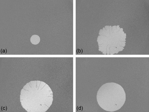
Figure 11.8b–d shows the subsequent DW propagation from the small reversed domain under different fields μ0H = 0.1, 0.6 and 1 mT, respectively. It is worth noting that DW propagation can be observed under fields as low as 0.1 mT. These fields are much lower than the nucleation field HN, which explains the sharpness of the hysteresis loops. This key result suggests that the strength and the density of pinning defects in our Ta–CoFeB–MgO films are relatively low, despite the very small thickness of the magnetic material. At very low fields μ0H < 0.6 mT, domain boundaries exhibit some jaggedness with the presence of 360° DWs, which indicates the presence of a distribution of pinning sites. However, the growth of nearly perfect circular domain at fields as low as μ0H = 1 mT, with only minor jaggedness along the domain boundaries, suggests again the presence of very weak random pinning sites. Note that this behavior has been observed for all the samples studied here, with only a slight difference in the field at which jaggedness vanishes.
11.3.2 Domain wall velocities
The velocity curves in the low fields regimen are shown in logarithmic scale in Figure 11.9a. The velocity is consistent with the creep theory (Ferré, 2002; Ravelosona, 2009; Lemerle et al., 1998; Blatter et al., 1994; Feigel'man et al., 1989) with velocity v(H) = v0Exp(βE(H)) where E(H) = UC(Hdep/H)1/4, UC is a scaling energy constant, Hdep is the depinning field, and β = 1/kBT. Here, Hdep can be estimated as the average field at which DW motion leaves the creep regime, which is between 2 and 3 mT for all samples as indicated in Table 11.2. This is a striking result because the values for Hdep in Co/Pt (Metaxas et al., 2007) or Co/Ni (Burrowes et al., 2010) films with similar magnetic properties (anisotropy and magnetization values) are typically one order of magnitude higher. The ln v versus H–1/4 dependence is consistent with the propagation of a 1-D domain wall in a 2-D weak random disorder. It is worth noting that the slope given by βUCHdep1/4 is slightly reduced for annealed samples of a given composition, which shows an increase of the energy barrier for DW motion. This is consistent with depinning fields that are found to be slightly higher for the annealed films. In ultrathin magnetic films, the pinning potential corresponds to a distribution of magnetic anisotropy at the nanometer scale (Ferré, 2002; Ravelosona, 2009), and this distribution may vary from amorphous to crystalline films as the average PMA increases. In particular, the presence of grain boundaries and crystalline texture in annealed CoFeB films may give rise to additional pinning. However, because Hdep also depends on magnetic parameters (Ferré, 2002; Ravelosona, 2009) such as the anisotropy and Ms values, it is difficult to give a final conclusion to the slight variation observed here. Finally, the low interface roughness, the low density of grain boundaries and the better structural coherence in amorphous and fully crystallized CoFeB films as compared with fcc textured films such as Co/Pt, Co/Pd or Co/Ni having similar magnetic properties could explain the low values of Hdep.

Table 11.2
Measured magnetic properties (depinning field Hdep and flow field Hflo) for CoFeB–MgO films with PMA
| Co20Fe60B20 As-deposited | Co20Fe60B20 annealed | Co40Fe40B20 As-deposited | Co40Fe40B20 annealed | Co60Fe20B20 annealed | |
| μ0Hdep (mT) | 2.5 | 3 | 2.5 | 2 | 3 |
| μ0Hflo (mT) | 11 | 12.5 | 7 | 10 | 6 |
| μ0HW (mT) theoretical | 0.3 | 1 | 0.3 | 0.8 | 0.3 |
Adapted from Burrowes et al. (2013).
Walker fields have been calculated using the 1D model and experimentally determined parameters (see Table 11.1).
The high fields dependence of the wall velocity for the different composition and crystalline states are shown in Figure 11.9b. For four of the systems considered above the depinning field Hdep, the wall velocity increases almost linearly as a function of field up to a field Hflo, which is between 6 and 12.5 mT (see Table 11.2). Above Hflo the velocity reaches a plateau. The only exception involves as deposited samples of composition Co40Fe40B20 as deposited, where a broad peak in the velocity is observed above Hflo. Moreover, we observed that the DW velocity (the high mobility regimen slope and the maximum velocity) is slightly higher for the as-grown case than the annealed case for compositions Co40Fe40B20 and Co20Fe60B20.
In the following, we discuss the origin of the two high fields’ motion regimens beyond the creep region, that is, (i) Hdep < H < Hflo and (ii) H > Hflo. In the flow regimen motion, the 1-D model predicts (Metaxas et al., 2007; Schryer and Walker, 1974) steady and precessional linear regimens separated by the Walker field HW. From the material parameters in Table 11.1, it is possible to evaluate the theoretical Walker field HW. To compute the Walker field, we use the relation (Schryer and Walker, 1974) HW = NyMs α /2 , where Ny is the demagnetizing factor across the wall given as (tCoFeB/tCoFeB + Δ) and Δ is the domain wall width that can be calculated as Δ = (A/Keff + Nyμ0Ms2/2)1/2. The low value of the damping parameters in our films leads to very low values of the Walker field HW ranging from 0.3 to 0.8 mT, which are 50 times lower than those of Co/Pt films (Metaxas et al., 2007). As a result of such low values, the Walker breakdown field lies inside the creep regimen, that is HW < < Hdep and is masked by the creep process. The intermediate regime Hdep < H < Hflo, which exhibits a very low wall mobility, is likely a transitory thermally activated depinning regimen with a linear energy barrier consistent with theoretical predictions (Gorchon et al., 2014). Note that Hflo is slightly higher for annealed films, which again indicate more pinning in the crystalline state.
The velocity plateau above the depinning transition corresponds to the low mobility regimen above Walker breakdown. This behavior has been confirmed with the 1-D model and micromagnetics simulations performed with the MuMax code (Vansteenkiste and Van de Wiele, 2011). Particularly, transverse instabilities (Yamada, 2011) in the wall structure are found to occur in the plateau at low applied fields, whereas at larger applied fields, the wall structure becomes more stable and a coherent magnetization precession is observed across the entire wall structure, which results in the linear increase in the wall velocity with applied field.
11.4 Domain wall pinning in magnetic wires
An important parameter that will ultimately determine the scalability of racetrack memory devices is the density and strength of pinning defects experienced by the domain wall when it propagates along the wire. The pinning potential originates not only from structural inhomogeneities in the magnetic films as described in Sections 11.2.2 and 11.3.2 but also from defects introduced by the lithography process such as, for instance, edge roughness. The average distance between strong pinning sites is an important parameter for determining the scalability of this technology because multiple DWs have to propagate on micron distances. In this section, we describe the characterization of the pinning potential on the nanoscale using Scanning nitrogen-vacancy (NV) center microscopy as well as micromagnetics simulations to show the importance of edge roughness on DW motion.
11.4.1 Characterizing the pinning potential using NV center microscopy
NV center microscopy is a powerful magnetic imaging technique that allows quantitative measurements of the stray magnetic field generated by a micromagnetic structure (Chernobrod and Berman, 2005; Taylor et al., 2008; Degen, 2008; Balasubramanian et al., 2008; Rondin et al., In press; Maze et al., 2008). This technique, which provides high sensitivity and allows for a spatial resolution ultimately limited by the atomic size of the probe, has recently enabled stray field imaging of nanoscale magnetic structures (Grinolds et al., 2013; Rondin et al., 2012, 2013; Tetienne et al., 2013).
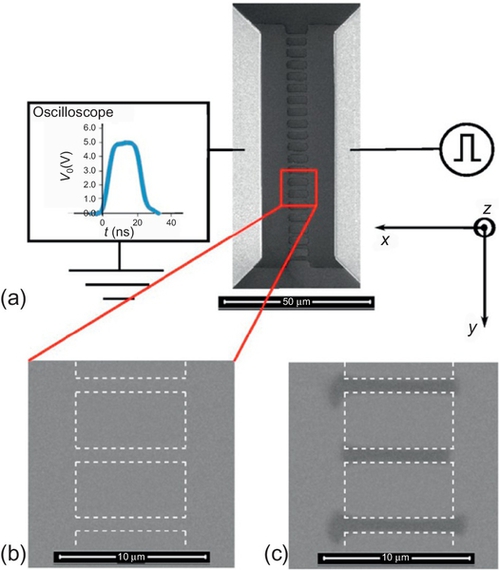
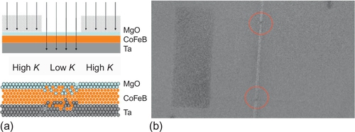
To have more insight about pinning sites in magnetic wires, we have used scanning NV-center microscopy (Figure 11.10) to image domain walls with a spatial resolution better than 100 nm (Tetienne et al., 2014). The scanning NV center microscope employs the electronic spin of a single NV defect hosted in a diamond nanocrystal, which is attached to the tip of an atomic force microscope and used as a magnetic field sensor. The magnetic field is evaluated within an atomic size detection volume by encoding Zeeman shifts of the electron spin sublevels onto the spin-dependent photoluminescence (PL) intensity of the NV defect. To this end, a laser beam at the wavelength λ = 532 nm is tightly focused onto the NV defect with a high numerical aperture microscope objective, while a radiofrequency (RF) source allows for manipulation of its electron spin state. The spin-dependent red PL intensity of the NV defect is collected by the same objective and forms the magnetometer signal, which gives information about the projection |BNV| of the local magnetic field along the NV center’s quantization axis uNV.

By combining this imaging capability with laser control of the DW position, we have directly observed DW hopping between pinning sites (Barkhausen jumps) and map the available sites over micrometer length scales. As seen in Figure 11.11, we first scanned the sample with a high laser power (> 1 mW) to drag the DW by thermal induced effect along the wire while monitoring its position at the same time (Figure 11.11a). Starting from the DW in site 1, the DW is indeed forced to follow the scan direction. In Figure 11.11b, at least six pinning sites can be identified. It is then possible to prepare the DW in a given pinning site by simply turning the laser off as soon as the DW is in the desired site. Then we have been able to image the DW with no significant perturbation by employing a low laser power (250 μW). Figure 11.11c shows images of the six stable or metastable pinning sites found in the 2-μm-long wire portion investigated. Apart from site 2, which relaxes towards site 1 with a characteristic time of 10 min (Barkhausen jumps), the other five sites were found to be very stable. The mean spacing between consecutive stable pinning sites is about 50–500 nm, with a maximum of 500 nm observed between sites 3 and 4.

These results confirm the very low density of pinning defects in Ta–CoFeB–MgO materials, which is much better than any other films with PMA such as Co/Pt, Co/Pd or Co/Ni. However, to make this material compatible with the ultimate technological node, it would be necessary to further reduce the density of defects because the racetrack memory involves wires of a few tens of micrometer in length. Finally, beside the great potential of NV center microscopy for studying thermally driven process of magnetic nano-objects, the possibility to drive the domain wall on the nanoscale with laser opens perspective for a new class of spintronics devices.
11.4.2 Influence of edge roughness
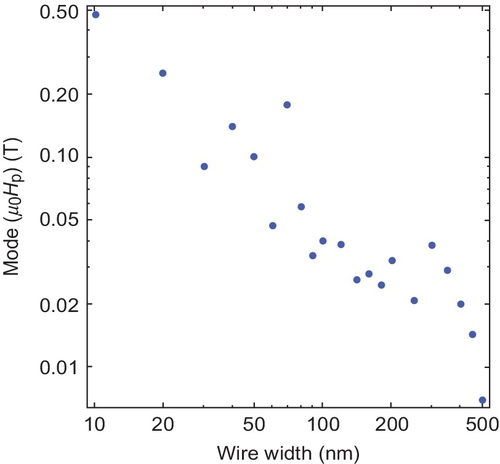
Because the density of intrinsic defects is very low in Ta–CoFeB–MgO materials, extrinsic defects introduced by the patterning techniques may reveal crucial, particularly for the scalability, issues. We have investigated the role of edge roughness on field-driven wall propagation through micromagnetics simulations using the MuMax code (Vansteenkiste and Van de Wiele, 2011). This code is based on the finite-difference method for solving the Landau–Lifshitz equation but utilizes fast algorithms and runs on graphics processor units (GPUs), which allows an increase of its performance up to 100 × over standard CPU-based codes, such as OOMMF. These simulations were conducted on wires of varying width (from 25 to 500 nm), which allows us to study the scalability issues of DW motion. The aim has been to quantify how the edge roughness influences the propagation field in such geometries (Figure 11.12).

The final results are presented in Figure 11.13. Although the simulations do not account for the intrinsic domain wall pinning that arises from material defects as described in Section 11.4.1, they describe the behavior expected due to edge roughness alone. As experimentally seen previously in CoNi multilayers with PMA, a large increase of the average propagation field is found when reducing the wire width down to 20 nm. Although the edge roughness here is very low (2–3 nm), this may be an issue for the scalability of this technology down to the ultimate node.
11.5 Mechanism of current-induced domain wall motion
To realize devices based on current-induced domain wall motion, key operations are the “writing”, that is, the nucleation of magnetic domain walls and magnetic domains in the wires and the “manipulation”, that is, the displacement of the magnetic domain walls under current and thereby the magnetic domains.
11.5.1 Generating domain walls using Oersted fields
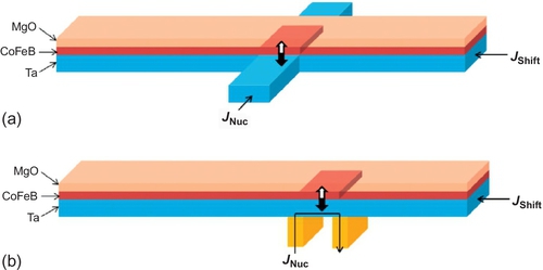
There are different approaches to nucleating domains and domain walls. The simplest is the conventional approach using Oersted fields generated by current passing through striplines. As seen in Figures 11.14a and 11.6a, this can be achieved by combining the magnetic wires with a low resistivity and thus low heating and ohmic losses Oe field line (stripline).

To calculate the resulting fields, numerical integration of the current paths is carried out. Figure 11.15a shows a small rectangle, whose width and height are the same as in the experiment representing a cross-sectional area of a gold Oe field line (1.4 μm (width W) × 150 nm (thickness H)). For the simulation of a local Oe field, we assume a fixed current density of 1 × 10¹² A/m2 being perpendicular to the plane of the nanowire, which is a reasonable density that is compatible with reliable operation based on our experimental results. In particular using these values, we obtain 100% DW nucleation probability using this current density (see below). The arrows in Figure 11.15 indicate the direction of the Oe field, and the color indicates the component of the magnetic field, which is perpendicular to the wire. A line scan along the top of the wire (a red line) shows this magnetic field component in Figure 11.15b as a function of its position along the wire. A sufficient high magnetic field for magnetization reversal is created in the surrounding of the gold Oe field line. The localized Oe field resulting has field strengths going up from 5 to 90 mT for distances from 10 μm from the gold Oe field line to the edge of the line. Therefore, a localized nucleation of a single domain wall in an out-of-plane magnetized wire is possible for soft materials such as CoFeB-based structures with low coercivity.

To gage the scalability of this writing approach using the Oe field line, we calculate the writing energy and the generated Oe fields for various dimensions as shown in Figure 11.16. Assuming a length of a gold Oe field line of 160 nm (for applications, we assume a design rule of 32 nm and the length is thus five times this design rule), we can calculate the power necessary for writing a single bit by taking into account the results from the simulations. Figure 11.16a shows the calculated resistance for a gold Oe field and the calculated energy for a constant current density of 1 × 10¹² A/m2 as a function of the cross-sectional area of the gold line. The writing energy is a few pJ at j = 1 × 10¹² A/m2 and is reduced as the cross-sectional area of a gold Oe field line is reduced. Figure 11.16b shows the calculated Oe fields for a current density of 1 × 10¹² A/m2 along the gold line for various dimensions. The Oe fields that can be generated are up to 15 mT for 100 nm wire width and 2 mT for a 20 nm wire width, which is compatible with future design rules that continuously scale to smaller dimensions. This field is still sufficient to realize magnetization switching in specially designed nanowires when a sufficiently low coercivity is achieved for a tailored material.

Next we study this DW nucleation experimentally. As shown in Figure 11.14, we can either determine the necessary current densities by directly imaging the nucleated domains and domain walls (device from Figure 11.14) or by electrically detecting the walls (Figure 11.6a) (Boulle et al., 2008). In the latter case, the DW is detected by the extraordinary Hall effect (EHE) resistance that shows changes when the DW is pinned at the Hall cross (Heinen et al., 2012). Figure 11.17 shows the EHE hysteresis of the Ta/CoFeB/MgO with and without a DW and indicates schematically the resulting magnetization configuration in the nanostructure. The black curve is the normal hysteresis of the Ta/CoFeB/MgO nanowire without a DW, and the blue one shows the hysteresis of Ta/CoFeB/MgO when a DW is nucleated. The coercivity changes drastically in the case where a DW is nucleated from Hc≈ 25-30 mT (normal hysteresis loop without DW) to HcDW ≈ 13 mT. After nucleating the domain wall close to the Oe field line, we see that the domain wall moves to the Hall cross at a propagation field Hprop of 3 mT. It then takes 13 mT to move the DW across the Hall cross to reverse the magnetization. The increased field of 25–30 mT without a nucleated domain wall means that the nucleation field for a DW is much higher than the propagation field and even the field needed to push the domain wall across the Hall cross.

The protocol for this measurement is that we first saturate the sample in one direction with a negative field (here marked as down magnetization indicated in blue in the schematic representations of the magnetization in Figure 11.17). Then the current pulse is injected through the gold Oe field line for DW nucleation at point (2) in Figure 11.17. The DW is nucleated in the nanowire using the local Oe field generated by current at pulse current density of 8 × 10¹¹ A/m2 and pulse length of 100 μs without any external field. Then there is a DW present in the wire close to the Oe field line (Figure 11.17 (3)) and this DW is propagated to the Hall cross at 3 mT external field. Figure 11.17 (4) shows the DW at the Hall cross, and the hysteresis shows small changes in the signal as the DW moves in the Hall cross and then when the coercivity field HcDWis reached, the DW moves completely across the Hall cross (Figure 11.17 (5)), and finally the samples are saturated in the up magnetization direction (Figure 11.17 (6)).
Next we study this nucleation systematically. We determine the DW nucleation probability, for two different current densities as a function of pulse length. All measurements shown in Figure 11.18 were repeated 10 times. At a current density of 5.64 × 10¹¹ A/m2, only 10% of the time DW nucleation is achieved without any external field. At a higher current density of 6.3 × 10¹¹ A/m2, we can obtain 100% DW nucleation probability without any external field as shown in Figure 11.18b.
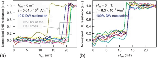
Figure 11.19 finally shows the DW nucleation probability for different current pulse widths from 1 to 10 ns. The DW nucleation probability increases with increasing the current pulse width. In particular we can obtain 100% for pulse lengths down to 2 ns and possibly lower (the limitation of the pulse shape, due to the equipment used, did not allow us to obtain results for 1 ns for higher current densities).

11.5.2 Manipulating magnetization by spin–orbit torques
Recently, it was shown that more efficient current-induced domain wall (CIDW) motion can be obtained in asymmetric magnetic multilayers due to novel spin–orbit torques compared to conventional spin-transfer torques (Boulle, 2011). A first observation of the spin–orbit torque on the DW motion in Pt/Co/AlOx nanowire was suggested by Miron et al. (2010), as the presence of structure inversion asymmetry (SIA) gives rise to an effective field (due to the Rashba effect, Gambardella et al., 2011) perpendicular to both the current flow direction and the magnetic easy-axis, which makes it energetically easier to rotate the magnetization inside the magnetic layer so that DW velocities have been detected up to 400 m/s. Another possible origin for such spin–orbit torque was suggested by Manchon (2012), who suggested as the origin of the high DW velocity the spin Hall effect (SHE) occurring in the SIA-stack when an electric current is injected through it.
Recently, another contribution necessary for the fast CIDW motion has been explored theoretically and experimentally, namely the Dzyaloshinskii–Moriya interaction (DMI) (Thiaville et al., 2012; Emori et al., 2013a,b; Boulle et al., 2013; Ryu et al., 2013). It was realized that the spin–orbit torques are not sufficient to move a domain wall that is usually a Bloch wall but one needs Néel DWs all with the same chirality, so that the SHE torque efficiency is maximized and synchronous motion is obtained. This combination of SHE and DMI is thus the real trigger of the fast CIDW motion in magnetic nanostructures with SIA. Furthermore, switching of the magnetization by spin–orbit torques has been observed (Liu et al., 2012). Such switching can be used to reverse the magnetization and thus also to “write” information by nucleating new domains and domain walls.
Figure 11.20 shows two different geometries to generate a spin current through Ta and induce DW nucleation in the adjacent ferromagnetic layer. To investigate this approach to initiate locally DW nucleation, we have used 1-μm-wide and 10-μm-long wires as shown in Figure 11.21. We have measured the combination of longitudinal fields Hx along the wire and current to induce magnetization switching. The longitudinal fields are used to lower the switching barrier by tilting the magnetization. Figure 11.21c shows a typical result of magnetization switching at a current density of 4.02 × 10¹¹ A/m2 flowing in the wire with 100 ns pulse width and a longitudinal field of 200 Oe.
Furthermore, we find that we can achieve switching even at zero external field due to thermal fluctuations that lead to transient magnetization components along the wire onto which the spin–orbit torques act that lead to switching (Lo Conte et al., 2014).
11.5.3 Displacing domain walls using spin–orbit torques
Having established the generation (writing) of domain walls, we next turn to shifting them. As discussed earlier, the combination of the spin–orbit torques and the DMI lead to efficient displacement of domain walls. We determine the key properties, which is the strength of the DMI by measuring the DW velocity as a function of an applied magnetic field along the wire axis (x-direction) for fixed current densities (see Figure 11.22). First of all, both types of DW (↑↓ and ↓↑) are nucleated in the presaturated nanostructures by current-induced magnetization switching (see Figure 11.22a). Typical nucleation pulses used in the experiment have a current density ja ~ 1012 A/m2 and a duration Δt = 20 ns. Once the DWs are generated, they are displaced by injecting a burst (n = 1–20) of 20-ns-long current pulses with lower current densities (2.8–3.6 × 10¹¹ A/m2), as shown in Figure 11.22b. To calculate the DW velocity, the full width at half maximum of the current pulse is used as the time duration of a single pulse. For each current density–field amplitude combination, the measurement is repeated five times. The DW velocity as a function of the longitudinal field μ0Hx is shown in Figure 11.22c and d (symbols), respectively, for the ↓↑- and ↑↓-DWs. The graphs show that the DW velocity is strongly influenced by the presence of the longitudinal field.

While at zero field the velocity of both types of DWs is the same; in the presence of the field the two DWs move at different velocities. We observe a symmetric behavior of the DW velocity as a function of μ0Hx for the two types of DW, as shown in Figure 11.22e (solid symbols for the ↑↓-domain wall, empty symbols for the ↓↑-domain wall). The field at which the SOT is minimized, resulting in a stationary DW, is the so-called DMI effective field μ0HDMI = D/(MsΔ) (Emori et al., 2013b), where D is the DMI coefficient, and Δ is the DW width. Figure 11.22c–e shows that there is a range of in-plane longitudinal fields μ0Hx where the DW remains stationary (with zero or very small DW velocity compared to the velocities measured for larger longitudinal fields). This zero motion field range is not reproduced by the standard SOT-DWM model and was not discussed in some other experiments. To properly analyze the experimental data a more accurate model is needed, where this “pinning” effect is taken into account.
Because the reversal of the direction of the DW motion occurs for the low-velocity field range, a more detailed analysis of this behavior follows. The DMI-field is extracted by linearly fitting the experimental data in Figure 11.22e, for both types of DW and for both positive and negative current. Considering only the high velocity experimental data, the crossing of the two best-fitting lines for the ↑↓-DW data occurs at a longitudinal field value μ0Hx↑↓ –8.5 ± 1.8 mT, whereas for the ↓↑-DW the crossing occurs at μ0Hx↓↑ = + 7.0 ± 1.5 mT. Assuming the amplitude of the DMI field to be the average of the two fields (in absolute values) we obtain |μ0HDMI| = 7.8 ± 1.2 mT. All the errors correspond to one standard deviation. Because the DW width is Δ = 7 nm (Δ = (A/Keff)1/2, where we use A = 10–11 J/m, Yamada, 2011), μ0Hx↑↓ < 0 and μ0Hx↓↑ > 0, and knowing that Ta-θSH has a negative sign (Lo Conte et al., 2014) we obtain a DMI constant D = + 0.06 ± 0.01 mJ/m2.
11.5.4 Combined operation of writing and shifting domain walls
Finally we combine the writing by the Oe field and the shifting to demonstrate the combination of both. As seen in Figure 11.23, we can write and shift domain walls thus demonstrating the functionality of a shift register device. Note that in the last displacement (e), the bottom two walls reach the end of the wire and thus stop (due to the reduced current density as the wire widens into the pad) leading to a change in the domain length.

11.6 Electric field-induced DW motion in CoFeB–MgO stripes
In the quest of reducing power consumption in novel magnetic devices driven by a current, alternative ways of controlling the operation of magneto-electric devices is of paramount technological importance. In this context, electric field effects in ferromagnetic/oxide structures provide a new route to control domain wall (DW) dynamics with low power dissipation (Ohno, 2000; Weisheit et al., 2007). In this section, we describe gate voltage modulation of DW velocity in CoFeB–MgO materials.
11.6.1 E-Field magnetic devices
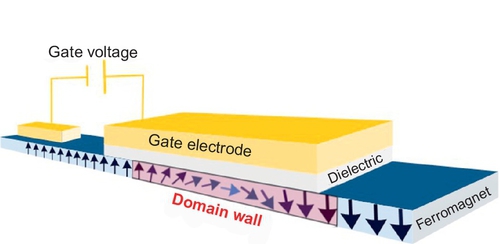
Electric field control of magnetic DW motion in transition metal ferromagnets has attracted great interest due to the possibility to achieve DW control with low power dissipation for memory and logic circuits (Schellekens et al., 2012; Chiba et al., 2012; Bauer et al., 2012, 2013, 2014; Bernand-Mantel et al., 2013; Herrera Diez et al., 2014). One promising approach is to use the E-field effect to produce anisotropy variation through charge modulation, which allows for the local manipulation of domain nucleation and domain wall motion processes. In Figure 11.24, a typical E-field domain wall device is represented. The E-field is generated by applying a voltage between the ferromagnetic and top gate electrodes across an insulating barrier. A key aspect in the device design is the ability to generate a considerable amount of charges in the ferromagnetic materials to modify the band filling. For 3-D ferromagnetic metals, the penetration depth for electric field is only a few angstroms, so that efficient electric field effect is favored only in ultrathin films exhibiting interface anisotropy. The induced charge density per unit area QA under an electric field E is QA = ɛ0ɛrE = ɛ0ɛrV/d , where ɛ0 and ɛr are the vacuum permitivity and the dielectric constant of the insulating barrier, V the applied gate voltage and, d the thickness of the insulating barrier. Consequently, a good device performance will be determined largely by the dielectric constant, quality and thickness of the insulating barrier.
Along this line, the electric field effect on DW dynamics has been demonstrated in Pt/Co/oxide ultrathin films with PMA involving oxides with relatively high dielectric constant (ɛr = 10–30) such as Al2O3, HfO2, or GdO (Chiba et al., 2012; Bauer et al., 2012, 2013, 2014; Bernand-Mantel et al., 2013). Liquid gates made of mobile ions in a liquid polymer matrix are also used due to their versatility and simple operation and incorporation into the magnetic device as well as for their dielectric constants that can take values up to ɛr = 66 (Weisheit et al., 2007; Herrera Diez et al., 2014). Oxides of gadolinium have also been used not only to support an E-field modulation of magnetic properties but also to provide nonvolatility of the effect through E-field-induced ion migration inside the oxide (Bauer et al., 2013, 2014).
11.6.2 E-Field control of domain wall nucleation and propagation
Domain wall velocity under electric field was measured in annealed Ta(5 nm)/Co40Fe40B20(1 nm)/MgO(2 nm)/TiO2(20 nm)/ITO using magneto-optic Kerr microscopy under combined electric and magnetic fields (Lin et al., 2014). By applying a top gate voltage VG between the bottom Ta/CoFeB and top ITO electrodes (shown schematically in Figure 11.25a), electrons can either accumulate or deplete at the CoFeB/MgO interface.
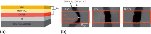
Figure 11.25b shows typical differential Kerr images of magnetic DW motion in applied perpendicular magnetic field pulses in an annealed CoFeB structure for various VG. The dark regions indicate the motion of the DW under the magnetic field pulse. The right and left boundaries in the dark part of the image show the DW position before and after, respectively, applying the magnetic field pulse. The VG was applied in the region of the 50-μm-wide ITO strip as indicated by the dashed rectangle. As shown in Figure 11.25b, at μ0H = 2.6 mT for Δt = 1 s, the DW displacement below the ITO strip at VG = − 1 V is smaller than that at VG = 0 V, whereas the DW displacement at VG = 1 V is larger. These results demonstrate that the DW velocities decrease as applying negative VG and increase as applying positive VG. Figure 11.26 shows the dependence of DW velocity on the gate voltage for different values of the magnetic field μ0H. In all field ranges, the DW velocity increases linearly with VG. In the low-field regimen, the effect of gate voltage on DW velocity is found to be relatively large (factor of 10 from − 2 to + 1 V at 2.6 mT) but it strongly decreases (factor of 1.1 from –2 to + 1 V at 28.7 mT) with increasing magnetic field.

To determine the role of voltage on the various dynamic regimens, Figure 11.27 shows the dependence of DW velocity v on the applied magnetic field H for typical gate voltages VG = − 1.5, 0, and 1.5 V. For the annealed sample, three DW dynamical regimens are observed including the creep, intermediate depinning and depinning regimens. In all regimens the DW velocity increases (decreases) under positive (negative) voltage in this annealed sample. In the creep regimen where μ0H < 8 mT (Figure 11.27b), the DW velocity can be expressed as

where UC is a characteristic energy related to the disorder-induced pinning potential, kB the Boltzmann constant, T the temperature, and Hdep the depinning field. The exponent 1/4 fits the data well and as shown before is theoretically predicted for interactions of one-dimensional DWs with two-dimensional weak random disorder in thin magnetic films with PMA. In agreement with Gorchon et al. (2014), close below Hdep a critical depinning regimen is observed for μ0H > 12 mT, where the velocity fits as,

This regimen allows us to determine accurately the value of Hdep for the gate voltages VG = − 1.5, 0, and 1.5 V. We find, respectively, μ0Hdep(–1.5 V) = 12.9 mT, μ0Hdep(0 V) = 11.7 mT and μ0Hdep(1.5 V) = 11.2 mT. These results are consistent with Figure 11.25, where a negative (positive) voltage impedes (favors) DW motion. Between these two regimens for 8 mT < μ0H < 12 mT, an intermediate depinning regimen occurs compatible with a thermally activated flux flow (TAFF) mechanism.
Here, the dielectric layer consists of a 2-nm-thick MgO (dielectric constant ɛMgO ~ 9.7) and 20-nm-thick TiO2 (dielectric constant ɛTiO2 ~ 100) films. A positive (negative) gate voltage of VG = + 1 V (− 1 V) corresponds to an electric field of ~ 2.5 × 10⁸ V m–1 and an accumulation (depletion) of ~ 0.01 electron per Co(Fe) atom at the CoFeB/MgO interface. Interestingly, it has been shown recently that electron accumulation can give rise to a reduction of PMA in Ta/CoFeB/MgO structures (Mantovan et al., 2013; Lamperti et al., 2013; Balasubramanian et al., 2008; Rondin et al., In press). The results here show that electron accumulation under positive voltage at the CoFeB/MgO interface increases the DW velocity. In the creep, intermediate depinning and depinning regimen, the increase of DW velocity under positive voltage is then consistent with a reduction of the energy barrier when the PMA decreases. Finally, we have demonstrated a universal description of this effect over the full range of DW dynamics by taking into account an effective magnetic field being linear with the electric field.
11.7 Control of the pinning potential in CoFeB–MgO nanostructures
As we have shown in the previous sections, the presence of defects can result in considerable pinning that impedes DWs propagation. This pinning effect has two important consequences. First, it introduces stochastic effects, whereby thermally driven processes involving hopping over energy barriers become important. Second, these processes can involve deformations in the DW profile itself, resulting in more complex two-dimensional dynamics. It is therefore an important challenge to develop artificial pinning potential to store efficiently DW at specified positions in the wire. In a previous approach (Burrowes et al., 2010), we used narrow constrictions as shown in Figure 11.7b to pin domain walls. However, this approach exhibits two main drawbacks. On the one hand, narrow constrictions induce deformations in the DW profile (Figure 11.28), and on the other hand, it is a big challenge to lithographically develop a series of similar constrictions along a magnetic wire for ultimate technological node.

One of the most promising schemes for DW storage if one takes into account the compatibility with manufacturing schemes is to reduce locally the perpendicular magnetic anisotropy, which induces an energy barrier for DW motion. It can be estimated that if the reduction of the perpendicular anisotropy is > 25%, then the energy wells achievable can be of the order of a few thousand milli-electron volt that is close to the ~ 60kBT threshold. In this section, we describe the possibility to introduce efficient pinning potential based on anisotropy contrast by using either ion irradiation through a mask or prepatterned substrates.
11.7.1 Ion irradiation through a mask
One elegant approach to control structural properties is to use light He ion irradiation that has demonstrated to be extremely efficient in controlling the magnetic properties of magnetic thin films and multilayers (Chappert et al., 1998; Ravelosona et al., 2000; Bernas et al., 2003; Fassbender et al., 2004; Cayssol et al., 2005). The low interaction cross section together with the low energy transfer lead to the absence of damage cascades, which induces short-range atomic displacements. This process allows a very precise control of magnetic properties through atomic short-range order modifications. Particularly, in Co/Pt multilayers, irradiation induced intermixing at interfaces allows the precise control of PMA.
In a precedent study (Barisic et al., 2013), we have demonstrated that Ta–Co20Fe60B20–MgO materials can be crystallized under ion irradiation at low annealing temperatures (< 100 °C) instead of a pure annealing process at high temperatures. Here, we have investigated the effect of light He+ ion irradiation at room temperature on the magnetic properties of crystalline Ta–Co20Fe60B20–MgO materials (Herrera Diez et al., 2015). As observed in Figure 11.29, a continuous reduction of ![]() under fluence can be obtained. Above 2.8 × 10¹⁵ ions/cm2, the magnetization goes from out of plane to in plane. Structural studies involving XRR and ToF-SIMS have shown that this reduction of PMA can be explained by a gradual intermixing of both Ta–CoFeB and CoFeB–MgO interfaces.
under fluence can be obtained. Above 2.8 × 10¹⁵ ions/cm2, the magnetization goes from out of plane to in plane. Structural studies involving XRR and ToF-SIMS have shown that this reduction of PMA can be explained by a gradual intermixing of both Ta–CoFeB and CoFeB–MgO interfaces.

We have applied this process to ion irradiation of magnetic wires through a mask (Figure 11.30) (Ravelosona). A fluence of 1.5 × 10¹⁵ ions/cm2 has been used to reduce locally the effective anisotropy by about 30%. The effect of ion irradiation on the DW depinning has been studied by Kerr microscopy as well as by scanning NV center microscopy. Two irradiated area of 1 × 1 μm2 (Figure 11.30b) has been created where two reversed domain walls are first easily nucleated at 6 mT due to a lower anisotropy in the irradiated area. Then a field higher than 20 mT is needed to depin these DWs and make them move in the nonirradiated area. Because DWs can propagate at fields lower than 1 mT in this material, this scheme is very promising in terms of efficient domain wall pinning with high thermal stability.
Because such a type of irradiated area can be generated with mask scalable to the limits of lithography, the ability to engineer pinning sites with ion irradiation is thought to be a viable solution to DWs storing in horizontal racetracks down to the ultimate node.
11.7.2 Prepatterned substrates
One alternative method to efficiently pin DWs consists of creating nanoscale steps in the substrates over which the Ta–CoFeB–MgO structure is grown (Diacomo). Eight inches SiO2 wafers have been treated to create a surface modulation made of parallel sub-nm steps with a period of 100 nm (see Figure 11.31). Very regularly spaced steps with a very low distribution of height and period have been obtained by using a combination of advanced nanotechnology CMOS processes involving the selective etching process of SiO2 and SiN materials, nanolithography and chemical mechanical polishing. This process is compatible with large-scale mass production. Two different step heights (h) have been realized as measured by AFM: high steps (HS) with h = 0.76(3) nm, and low steps (LS) with h = 0.25(4) nm. Following the realization of the prepatterned substrates, Ta(2 nm)/Co40Fe40B20(1 nm)/MgO(2 nm)/Ta(5 nm) stacks have been deposited at room temperature. Strong perpendicular anisotropy is observed on both HS and LS substrates, as-deposited and annealed. This is an important result, which extends the already established possibility to achieve PMA uniformly on treated 8″ SiN/SiO2 substrates (Mantovan et al., 2013). Despite the nm-scale thickness of the CoFeB layer, high-quality films still showing PMA can be deposited on the nanoscale-modulated surface as well. At the step edges, a local variation of magnetic anisotropy and probably also exchange is expected.

Kerr microscopy has been conducted by measuring the DW velocity both along and across the steps (Figure 11.32). In the amorphous case, for both HS and LS substrates, the DW velocity is reduced by up to two orders of magnitude when the DW wall propagates across the steps. This indicates that the steps impede DW motion as expected. Following thermal annealing, in both cases, DWs’ motion cannot move across the steps and only flows preferably along them. This is an indication that the energy barrier has been increased largely, and that the steps acted as ideal pinning sites.

Depinning fields Hp = 1.8 mT, in the case of DWs moving along the steps in amorphous samples, are comparable (even lower) than those obtained for similar stacks on top of flat substrates. On top of higher steps, Hp reaches 6.8 mT for DWs moving across the steps in the amorphous film, being much higher than the 1.8 mT value for the DWs moving along the steps, in the same sample. Because such types of steps can be generated with a pitch scalable to the limits of lithography, the ability to engineer pinning sites with prepatterning substrates is also thought a viable solution to DWs storing in horizontal racetracks.
11.8 Circuit architectures for nonvolatile memories based on DW motion in nanowires
As mentioned earlier, domain wall motion in perpendicular magnetic anisotropy nanowires promises higher performance (i.e., power, speed and density) for data storage compared to the conventional nonvolatile memories. However, the integration circuits and architectures are much complex, which dominates the storage density and power. In this chapter, we present examples of circuit architectures to integrate DW motion in magnetic nanowires, including its peripheral circuits and some specific embedded architecture such as magnetic content addressable memory (CAM) and reconfigurable configuration storage.
11.8.1 Peripheral circuits to translate the signals between “Spin” and “Charge”
First, peripheral circuits are needed to translate the data between “spin” and “charge”, which are represented, respectively, by the direction of magnetization in the magnetic nanowire and the digital input/output (see Figure 11.33) (Zhang et al., 2012a). For this purpose, we have developed three circuits for domain wall nucleation, propagation and detection. Figure 11.33a shows a simple example of the peripheral circuits, where a couple of inverters (PMOS transistors MP1-2, NMOS transistors MN1-2) are used to generate bidirectional currents Iw and to nucleate magnetic domains in the write head MTJ0 (Zhang et al., 2012b). The NMOS transistor MN3 generates a unidirectional current to move the domain wall, and an ultrasensitive sense amplifier CMOS circuit (SA) is used to detect the magnetization in the read head MTJ1 through the current Ir. For the nucleation through spin transfer torque, a number of circuit solutions have been proposed to overcome stochastic behaviors and breakdown voltage (Lakys et al., 2012). But it is still a big challenge for the SA as the TMR is relatively low, and the process variation affects greatly the read error rate. Besides the read current Ir can also write erroneously the magnetization in the read head.
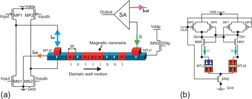
Figure 11.33b shows an example of SA based on precharge mechanism (PCSA) (Zhao et al., 2009) to avoid high sensing power of static sensing methods and provides the maximum hardness against the process variation. It consists of a precharge subcircuit (PMOS transistors MP2-3), a discharge subcircuit (NMOS transistor MN2) and a pair of inverters (NMOS transistors MN0-1 and MP0-1), which act as an amplifier. Its two branches are normally connected to a couple of MTJs with complementary states. It operates in two phases: “Precharge” and “Evaluation”. During the first phase, “CLK” is set to “0” and the outputs (“Qm” and “/Qm”) are pulled up to “Vdd” or logic “1” through MP2-3, whereas MN2 remains off. During the second phase, “CLK” becomes “1”, MP2-3 are turned off and MN2 on. Due to the resistance difference between the two branches, discharge currents are different. The lower resistance branch will be pulled down to reach more quickly the threshold voltage of the transistor (MP0 or MP1), at that time, the other branch will be pulled up to “Vdd” or logic “1” and this low-resistance branch will continue to drop to “Gnd” or logic “0”.
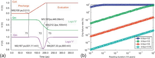
Figure 11.34a shows a sensing operation of PCSA (Zhao et al., 2012). The “Precharge” phase occurs before the moment “T”1. Both outputs are pulled up to 1 V. Then the “Evaluation” phase starts from “T1”, two branches begin to discharge after a small delay considering the rising time of “CLK” signal. At the time “T2”, the branch “Qm” reaches the threshold first, and this branch will continue to decrease to “0”. At the same time, MP2 begins to work and recharge the complementary branch “/Qm” back to “1”. This sensing operation is as fast as 100 ps. From the point of view of consumption energy, a sensing operation can only cost as low as 10 fJ. This high-speed and low-power feature makes PCSA suitable for the logic applications. From Eq. (11.3), we can estimate the chip error rate Fchip due to the erroneous switching of the read head, showing that the PCSA provides the lowest Fchip by reducing both the read current duration and value (Zhao et al., 2009).

where N is the number of bits per word, Ir is sensing current, IC0 is the critical current, τ is the read duration, and τ0 is the attempt period.
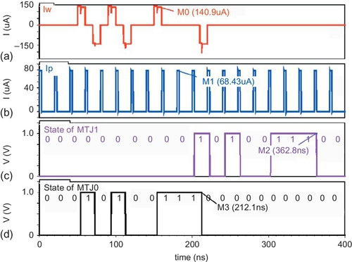
Based on the design of peripheral circuits, a complete racetrack memory can be built up and simulated. Figure 11.35 shows the transient simulation results driven by 50 MHz domain wall propagation current pulse Ip or Ish in Figure 11.33 is ~ 68.43 μA, and its duration is 2.5 ns (see Figure 11.35b). Initially, the states of all the storage elements in the magnetic nanotrack are set to “0”, and we plan to store a random logic pattern “…00010100111000…”. The pattern is first sent to write head MTJ0, and the domain wall nucleation current Iw, ~ 140 μA is activated during each data transition between logic “1” and “0” (see Figure 11.33a). Ip should be set to “0” during data nucleation to avoid leakage currents. After the data nucleation, Ip is activated to induce domain wall motion in the magnetic stripe, and we can obtain the same pattern at the read head MTJ1 after eight pulses (see Figure 11.35c–d). This simulation shows the correct operations of this PMA racetrack memory with low Iw and Ip, allowing small die area. However the speed, 50 MHz is relatively low for advanced computing logic circuits, where a short square wave is often used as the driving signal (e.g., CLK), for instance, 500 MHz square wave. In this case, we need the domain wall nucleation (~ 1 ns) and motion (~ 1 ns) in one cycle, higher amplitude current pulses Iw ~ 414 μA and Ip ~ 176 μA are, respectively, required. For this purpose, a large circuit area should be added, which reduces the storage density due to the trade-off between current value generation and channel width of CMOS transistors. Note that it is difficult to use a square wave to drive the in-plane anistrophy racetrack memory as the duration of domain wall nucleation is much longer than that of domain wall motion.
11.8.2 Innovative architectures for logic operations
Based on the peripheral circuits, we can explore innovative architecture of nonvolatile memory based on CIDW motion in nanowires to address different applications (Zhang et al., 2012c; Trinh et al., 2013; Zhao et al., 2011) such as magnetic content addressable memory (MCAM) (Zhang et al., 2012c) and multibit magnetic full adder (MFA) (Trinh et al., 2013). By applying a spice-compatible electrical model and advanced node CMOS design kit, power, speed and area performances of these hybrid architectures can be analyzed through mixed simulations to obtain the best design for specific applications.
Content addressable memory (CAM) is a computer memory that can output the address of search data. It compares search data with stored data and returns the match location with its high-speed fully parallel manner. Therefore it is widely used in mobile, Internet routers and processors to provide fast data access and ultrahigh density. The mainstream CAMs are composed of large-capacity volatile static random access memory (SRAM) blocks, which lead to high static power and large die area. These become the key challenges for the future R&D of fast data storage. Replacing volatile memories by nonvolatile memories or applying hybrid nonvolatile logic-in-memory circuits is a promising solution to build nonvolatile CAM and overcome both these drawbacks. We proposed an architecture design of CAM based on DW motion in PMA magnetic nanowires (MCAM). Its nonvolatile feature can reduce the static power caused by leakage currents. The CMOS-based DW nucleation and sensing circuits are globally shared to economize the cell area. The structure of complementary dual nanowires allows local sensing and fast data search operation.
The MCAM is composed of comparison circuits, PMA magnetic nanowires and DW nucleation/propagation circuits. A couple of complementary magnetic nanowires are used to present one word (see Figure 11.35a) to obtain the most reliable and fast access operation as this solution benefits from the maximum sensing marge compared with the conventional single nanowire structures. Due to different directions of the writing current pulse Iwrite through these two MTJs, they can nucleate the complementary configurations through STT switching mechanism under the same Iwrite pulse. One of the critical challenges for complementary magnetic nanowires is to synchronize precisely the DW positions. Here, the same current pulse Ipropagation moves magnetic domain walls in the dual nanowires, and we implement the DW pinning constrictions with the same distance in the magnetic nanowires. There are also a couple of PMA MTJs at each bit of storage elements as read heads. Because lower resistance can reduce the rate of breakdown and higher resistance can improve the sensing performance, the size of read heads should be smaller than that of write heads to obtain the best switching and sensing reliability.
The comparison circuit (see Figure 11.35b) consists of two parts: a PCSA detects the complementary magnetization of the read heads by using two reading current pluses (Iread and Ireadb) and outputs a logic value; the transistors MN3–MN6 build a classical NOR-type CAM. The signal “MLpre” is used to precharge the match line (ML). In case that the search line “SL” (“SLb” is its complementary signal) matches the stored data, there is no path to discharge and ML will thus be asserted. In contrast, ML will be discharged. By using a spice-compatible model of PMA racetrack memory (Zhang et al., 2012a) and STMicroelectronics CMOS 65 nm design kit, a DW-CAM has been simulated. Figure 11.35 shows the transient simulation results for “match case” (red) and “miss case” (blue). A 2-ns search operation can be found in these results. That means this DW motions-based CAM can operate at a 500 MHz frequency, which can be comparable to that of SRAM-based CAM (Figure 11.36).

Table 11.3 summarizes the comparison of CAMs based on different technologies. In addition to nonstatic power, MCAM shows a great advantage in terms of density thanks to 3-D integration and sharing of CMOS circuits.
Table 11.3
Comparison of CAMs based on different technologies
| Type | Area (F2/bit) | Cycle time (ns) | Energy (fJ/bit/search) | Static power |
| SRAM-CAM | 540 | 2 | 9.5 | Yes |
| MCAM | 19 | 0.45–2 | 12 | No |
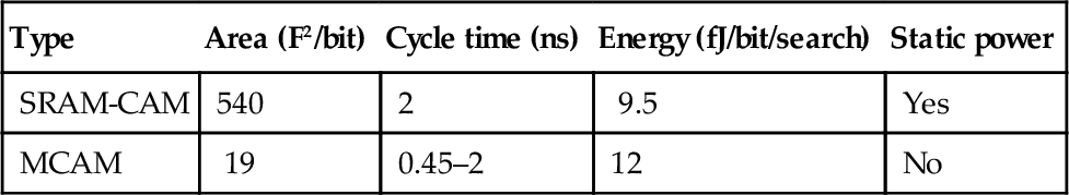
DW motions in magnetic nanowires are distinguished as they can both store and shift multiple bits of data. This advantageous feature makes them possible to design a high-speed and compact multibit serial magnetic full adder (MFA) (Zhang et al., 2012c). Figure 11.37 shows the detailed schematic of CARRY circuit of multibit MFA based on DW motion in nanowires, which is built on logic-in-memory architecture (Zhao et al., 2014). “A” and “B” are multibit input data stored in different nanowires. Each datum is designed to be stored in dual magnetic nanowires with exactly opposite configuration to minimize the variation between two complementary data (e.g., “A” and “![]() ”) as the same Ishift is used in the dual nanowires to move the DWs. At each rising edge of the clock (CLK), “Co” and “
”) as the same Ishift is used in the dual nanowires to move the DWs. At each rising edge of the clock (CLK), “Co” and “![]() ” are evaluated through the PCSA circuit and become inputs of a writing circuit, which generates writing current Iwrite to reverse or just conserve the state of nucleation MTJs (“Cnucleation” and “
” are evaluated through the PCSA circuit and become inputs of a writing circuit, which generates writing current Iwrite to reverse or just conserve the state of nucleation MTJs (“Cnucleation” and “![]() ”). At each falling edge of CLK, propagating current Ishift induces the DW motions of all magnetic nanowires (“A”, “
”). At each falling edge of CLK, propagating current Ishift induces the DW motions of all magnetic nanowires (“A”, “![]() ”, “B”, “
”, “B”, “![]() ”, “C”, “
”, “C”, “![]() ”) simultaneously and pushes next magnetic domains under the read MTJ for next adding operation.
”) simultaneously and pushes next magnetic domains under the read MTJ for next adding operation.

These bits are then shifted in a way that at the end of all additions, the sooner the bit is calculated, the greater its weight is. To validate its correct behavior, STMicroelectronics CMOS 65 nm design kit and a compact model of PMA racetrack memory have been used to perform SPICE simulations for this multibit MFA. The transient simulation shows the addition operation of two random 8-bit words: “A” = “01110011” (Figure 11.38b–c) and “B” = “01011010” (Figure 11.38b–d). “CLK” (Figure 11.38b–d) drives PCSA circuit and “Ishift” (Figure 11.38b) induces DW motions in the magnetic nanowires. The outputs “SUM” (Figure 11.38b–e) and “Co” (Figure 11.38b–f) are first precharged to logic “1” when “CLK” = “0”, and are evaluated when “CLK” is set to “1”. The DW motions are implemented in the precharge phase to avoid the disturbance to the output evaluation. The serial addition is performed from the least significant bit and the simulation result “SUM” = “11001101” and “Co” = “01110010” confirms the correct operation of MFA.
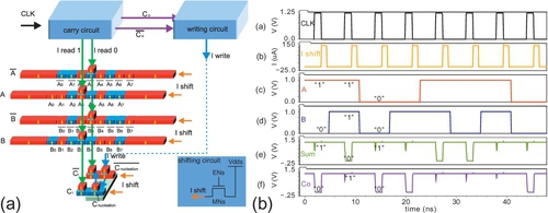
A comparison between the MFA and CMOS-only full adder is shown in Table 11.4. MFA shows advantages in terms of static energy, die area and dynamic energy while keeping latency at the same order.

11.9 Conclusion
Racetrack technology is one of the few emerging technologies that could be competitive with the incumbent NAND flash technology in terms of cell size. The introduction of thin magnetic layers with perpendicular magnetic anisotropy has opened the way to further scaling the technology. This chapter has covered the current understanding of DW propagation in CoFeB–MgO structures with perpendicular magnetic anisotropy. These structures exhibit a very low density of pinning defects due to their crystalline character, which makes them not only a good model system for fundamental studies of DW dynamics but also one promising system for applications to memory and logic devices. Particularly, the demonstration that domain walls can be manipulated by current, electric field effect or light provide a new route to extend the scaling of spintronic devices down to the nanometer scale. However, there remain important challenges to overcome. Among these are the demonstration of multiple domain wall motion in sub-20 nm devices, manufacturability issues and integration in CMOS technology. The next steps also involve a further understanding and optimization of spin–orbit coupling at interfaces. This has led to an innovative field of research called “spin–orbitronics” involving interfacial design of spintronic materials. This could lead, for instance, to efficient motion of magnetic skyrmions, which are less sensitive to defects than DWs. In addition, the nonvolatility, endurance and versatility of DW devices can also be extremely promising for alternative computing approaches such as neuromorphic circuits.