
Chapter 17
Liquid Crystals for Nanophotonics
17.1 Introduction
Integrating nanotechnology and liquid crystals (LCs) opens up a new area of hybrid research, which enables the realization of novel photonic devices and displays [1–7]. A study by Yeung et al. [1] showed the possibility of using nano-structured alignment surfaces based on a random distribution of vertical and horizontal polyimide domains (inhomogeneous layer) to align LC molecules for display applications. It was observed from the experiment that if the inhomogeneity was submicron in size, then there was no visible defect in the LCD and also that the layer takes on interesting properties that can be controlled by the properties of the domains. The nano-structured alignment surfaces can provide any pretilt angles between 0° and 90° and are useful for realizing zero-bias voltage π cells and bistable bend splay displays. Another major example of the application of nanotechnology to LCDs is the addition of nanoparticles to the LC [3–7]. Depending on the optical properties of the nanoparticles, which may be metallic, semiconducting or dielectric, the LC can take on different dispersive properties.
In this chapter, carbon nanotubes and LCs are integrated together to realize novel photonic devices to exploit the drastic size difference between the LC molecules (1–2 nm) and carbon nanotubes (a few nano to micro meters). This interaction can be interpreted as an interaction through the optical anisotropy of the LC [8, 9]. Hence, vertically grown carbon nanotubes electrodes in a LC can be used to form defect centers in the LC which then can be manipulated by applying an external electric field. The electric field confinement of the nanotube is of the same order as its height. So carbon nanotubes in the array are usually spaced at a distance twice their height to minimize electrostatic field shielding from the adjacent neighbors and to avoid the distortion of the photonic elements formed. The vertical height of the multi-wall carbon nanotubes in these arrays was typically 2–5 μm, which implies that the distance between two carbon nanotubes had to be at least 10 μm to ensure that there was no electrostatic repulsion between the field profiles of adjacent nanotubes to avoid distortion in the phase modulation.
This technology offers completely new ways of controlling molecules in LCs, allowing the crystals to move in a variety of directions to create optical components, such as nanophotonic lens arrays. LC molecules are shaped so that they naturally align with each other if put into a cell to form an optically active pixel. In a LC display device the LC pixel is used to change the polarization of the light passing through it and the degree of change (seen as contrast) is done through an applied voltage on electrodes at the top and bottom of the cell. The applied voltage makes the LC molecules rotate in the cell and changes their orientation with respect to the light passing through the cell. This cell geometry limits the ways in which the light can interact with the LC molecules on a two-dimensional (2D) plane. When a three-dimensional (3D) element is added to the lower electrode, it is possible to change the way in which the voltage interacts with the LC molecules to make a 3D optical structure. This means that it is possible to have a resolution of over 106 optical elements such as multi-wall carbon nanotubes up to 5 μm high on a 10 × 10 mm chip. For shorter multi-wall carbon nanotubes, even greater density nano and micro-optical arrays are possible within a very small volume.
17.2 Carbon Nanotubes
Carbon is the most versatile element in the periodic table because of the different arrangements of electrons around the nucleus of the atom and hence the number of bonds it can form with other elements. There exists three allotropic forms of carbon; graphite, diamond, and buckminsterfullerene. Graphite consists of layered planar sheets of sp2 hybridized carbon atoms bonded together in a hexagonal network. Diamond has a crystalline structure where each sp3 hybridized carbon atom is bonded with four others in a tetrahedral arrangement. The third allotrope buckminsterfullerene or fullerene (C60) is made up of spheroidal or cylindrical molecules with all the carbon atoms sp2 hybridized [10]. Smalley and co-workers [11] proposed the existence of a tubular form of fullerene termed a carbon nanotube. The experimental evidence of the existence of carbon nanotubes was discovered by Iijima [12] by imaging multi-walled carbon nanotubes using transmission electron microscopy. Iijima discovered single-walled carbon nanotubes as well two years later. A single-walled carbon nanotube can be considered as a rolled graphene sheet. Carbon nanotubes are one of the most promising materials for device fabrication because of their excellent electrical, thermal, and mechanical properties in addition to high aspect ratio and high resistance to chemical and physical attack.
Carbon nanotubes are metallic or semiconducting based on the exact way the carbon nanotubes are wrapped. Multi-wall carbon nanotubes are metallic in most cases as there are so many layers and the probability is very high of having one wrapped layer in the group to being metallic.
17.3 Uniform Patterned Growth of Multi-wall Carbon Nanotubes
Carbon nanotubes find applications in the areas, such as micro electronics, field emission displays, X-ray sources, and gas sensors. Single- and multi-walled carbon nanotubes can be grown using high-pressure arcs, laser ablation, and chemical vapor deposition. It is essential to develop a process which enables high yield, highly uniform, perfectly aligned nanotubes at precise locations on the substrate in order to utilize their unique properties. The plasma-enhanced chemical vapor deposition (PECVD) technique was used [13] to grow uniform, perfectly aligned nanotubes on a Si substrate. The process of using PECVD along with lithographic patterning without the deposition of amorphous carbon (a–C) has been largely ignored in the literature. A study by Teo et al. [14] showed the impact of the C2H2:NH3 ratio in the growth of the carbon nanotubes and a–C deposition in the conventional PECVD technique. The plasma is not necessary for the nucleation and growth of nanotubes, but the electric field induced by the plasma is required for the alignment of the nanotubes. The C2H2 provides carbon for the growth of the nanotubes, while the NH3 etches the carbon and hence a balance between the growth of the tubes and removal of a–C is achieved. The C2H2:NH3 ratio was varied from 15% to 75% in order to investigate the influence of the gas composition on the formation of a–C. The chemical composition of the unpatterned Si areas was investigated by Auger electron spectroscopy (using an in situ 2 keV Ar–ion gun). When the C2H2 ratio increased beyond 30%, a–C deposition also increased and they found a peak when it crossed 50%. An interface region of Si, C, N2, and O2 formed for all C2H2 concentrations. It was found that the optimal C2H2 ratio for clean nanotubes deposition lies between 15% and 30%. The thickness of the Ni thin film catalyst controls the diameter, height, and density of the nanotubes. The spacing between the nanotubes can be controlled through lithography and the height of the nanotubes by the deposition time of the tip growth mechanism. This pattern and growth method was used for growing uniform, patterned, multi-wall nanotubes in the nanophotonic devices.
Where V the voltage is applied across the electrodes and d is the gap spacing between the electrodes. If one of the electrodes is replaced by a sharp protrusion or a carbon nanotube, then d is interpreted as the minimum distance between the electrodes. So the local field (within 1–2 nm of the surface atoms) is much higher than the applied field. So the field is very high close to the tip and causes field emission of electrons above a threshold value. The shape of the electric field that spawns from the carbon nanotube in vacuum is also found to be near Gaussian [15].
17.4 Properties of LCs Exploited in Nanophotonic Devices
The main properties that are used in our device developments are birefringence, dielectric anisotropy, and fluid viscosity.
![]()
The speed of light in a medium is a direct function of the refractive index of that medium. Birefringent materials have refractive indices that are direction dependent. If the refractive indices for parallel and perpendicular polarized light are different within a material, then the light will travel at different velocities depending on its polarization (the orientation of the electric field) through the birefringent medium. Interaction between the light waves polarized parallely and perpendicular to the molecular axis, depends on the wavelength and gives rise to different colors when viewed through an optical microscope with white light. Dielectric anisotropy of LCs may be defined as the difference between the dielectric permittivities parallel and perpendicular to the director. Interaction of a LC with the external electric field is very much dependent on their dielectric properties.
17.5 The Optics of Nematic Liquid Crystals
The nematic mesophase is one of the most common calimatic (rod-like) LC mesophases [16]. A large birefringence and a low control voltage distinguish the nematic phase from other electro optical materials. The molecules in the nematic phase only have long range order and no longitudinal order (i.e. do not form layers). This is the least ordered mesophase before the isotropic. The calimatic molecular shape gives order in the nematic phase, which means that on the average the molecules spend slightly less time spinning about their long axis than they do about their light short axis.
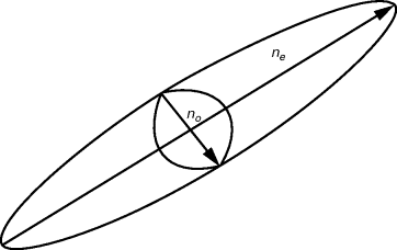
The optical indicatrix or index ellipsoid of a LC is a 3D structure to represent the variation of the velocity of light passing through it with respect to the molecular director. When light enters a birefringent material like a LC, its electric field is split into two orthogonal components termed ordinary and extra ordinary rays corresponding to the ordinary refractive index (no) and extra ordinary refractive index (ne) as shown in Figure 17.1. In the case of uniaxial samples, one of the components lies on the equatorial plane and always has the same value, called ordinary component. The other component varies with the angle of incidence and is known as the extra ordinary component. All these parameters are bulk parameters, which are estimated by taking the statistical average across billions of individual molecules.
Figure 17.1 Refractive indicatrix of a nematic LC molecule.
If the optical indicatrix is oriented at an angle θ to the plane of the cell such as the plane of the glass walls and ITO electrodes, then the refractive index seen by light passing perpendicular to the cell wall is given by
(17.1) ![]()
From the above equation, the optical retardance Γ can be calculated for a given sample of thickness d and at a wavelength λ when the material is oriented at an angle θ to the light polarization direction.
(17.2) ![]()
17.6 LC Hybrid Systems Doped With Nanotechnology
Commercial manufacturer of LC displays use a mixture of 5–10 LC compounds in order to have the appropriate physical properties. The performance of a LC device mainly depends on the LC materials used. Therefore, much effort has been made to improve the electro-optical properties of the LC by introducing dopants, such as dyes and nano-particles [17]. Carbon-based nano particles (nanotubes) have been found promising because of the excellent electrical properties and strong interaction with the aromatic mesogenic groups of LCs. Alternatively, it was observed that, due to high electron affinity and large mobility of π electrons along the tubular axis of the nanotubes, there was an extremely high anisotropy of polarizibility, electrical, and electro-optic properties of the nematic LC/carbon nanotube suspensions. These are much closer to the desired properties for LC displays than the LC alone. Threshold voltage and response time are also critical concerns for a LC device. Low threshold voltage and fast response time result in a better performance for the optical device. Adding a small amount of high aspect ratio carbon nanotubes into the rod like LC mixture yields a good guest–host effect, and hence predictably modifies the absolute dielectric anisotropy as well as the viscosity of the LC–carbon nanotube mixture. These two parameters significantly affect the electro-optical effects of a LC device. Fuelled by both scientific interest and potential applications, carbon nanotube and LC-based suspensions are still of great interest.
The electro-optic properties of a LC can be modified by introducing nano-particles [3]. A study by Jeong et al. [4] showed the formation of unusual double four-lobe nematic textures in a multi-wall carbon nanotube doped LC under the application of an external voltage from 120 to 160 Vrms at 1 Hz. The LC cell was prepared using two glass substrates with inner ITO electrode coatings filled with Merck (MJ951160, positive dielectric anisotropy) and a cell gap of 60 μm. Multi-wall carbon nanotubes having diameters around 3–6 nm and lengths of around 250 nm were first dissolved (10−3 wt.%) in dichloroethane and then mixed with the nematic LC. The prepared cell was characterized between crossed polarizers under the application of an external electric field. A perfect dark state was observed at low voltages. When the voltage increased, light started leaking through the crossed polarizers. A four-lobe texture appeared at 60 Vrms threshold voltage due to the director deformation inside the LC caused by the motion of the carbon nanotubes.
A study by Baik et al. [5] showed the local deformation of the LC director introduced by translational motion of carbon nanotubes in a plane field. The LC molecules were homogeneously aligned in the cell. Single wall carbon nanotubes having diameter less than 3 nm with a bundle size of tens of nanometers were doped (5 × 10⁻⁴ wt.%) in a LC medium. Inter-digitated opaque aluminum electrodes were placed on the bottom substrate, having width and thickness of 10 μm and 30 μm, respectively. The cell was observed between crossed polarizers under an external applied voltage. Two vertical stripes started to appear after a threshold voltage of around 60 Vrms due the motion of the carbon. The motion of the carbon nanotubes is explained below. The carbon nanotubes can hold a net charge due to a permanent dipole moment. This net charge can overcome the LC director field locally and hence the movement of the nanotubes.
The electro-optical characteristics of carbon nanotube doped LC devices were investigated by Huang et al. [6]. The threshold voltages and switching behavior of the device were measured and discussed. The measured results revealed that anisotropic carbon nanosolids modified the dielectric anisotropy and the viscosity of the LC–carbon nanotube mixture which changed the threshold voltage and the switching behavior of the LC device. Carbon nanotube doped LC devices with two complementary structures were considered; twisted nematic (TN) and chiral homeotropic LC (CHLC).
17.7 Carbon Nanotubes as Electrode Structures
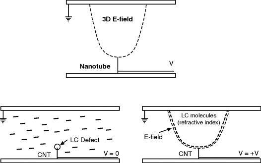
A traditional device structure such as a LC display pixel is based on a parallel plate capacitor design with top and bottom electrodes aligned to give a uniform electric field profile across the LC cell. Vertically grown multi-wall carbon nanotubes allow us to break this uniform structure and create a true 3D electric field profile. If a MWCNT is grown with more than three concentric skins of grapheme then there is a 99.999% chance that it will be conducting. A typical MWCNT used here would be 50 m in diameter which equates to roughly seven skins, hence we can assume that all of the tubes will be conductors and act as very fine wires grown vertically from the substrate. Using the PECVD process [14] arrays of electrodes have been made from individual vertically aligned multi-wall carbon nanotubes which are then used to address a layer of nematic LC. The nanotube electrodes create a near-Gaussian electric field profile which is used to reorient a planar aligned nematic LC. The variation in refractive index within the LC layer acts like a graded index optical element which can be varied by changing the applied electric field to the carbon nanotube.
When individual MWCNTs are subjected to an applied electrical potential, they form an electric field profile from the tube tip to the ground plane which is approximately Gaussian in shape [15] as indicated by the dotted line in Figure 17.2(a). If the nanotube electrodes are immersed in a planar aligned nematic LC material as shown in Figure 17.2(b) with no field applied, then the LC molecules would align parallel to the upper substrate surfaces due to the planar alignment provided by rubbing a surface coating, such as a thin film of polyimide. When an electric field is applied to the cell shown in Figure 17.2(c), then the molecules of the LC align to the electric field due to their dielectric anisotropy and freedom to flow. The electric field profile is approximately Gaussian in shape and the LC molecules will align to this field (assuming in this case a positive dielectric anisotropy) creating a torque about the long molecular axis which causes them to rotate. The final orientation of the LC is quite complex due to the Gaussian field profile combined with the surface effects of the alignment layer applied to the upper substrate of the cell. The resulting combination of these two effects creates a varying (or graded) refractive index profile across the cell. The profile formed is in effect a micro-optical element due to the gradient index profile across the reoriented LC. If the graded index were Gaussian, then this would form a microlens capable of focussing an applied light wave. More importantly, the micro-optical elements can be tuned by varying the applied field and therefore reorienting the LC and varying the optical properties of the microlens. The optical element formed is similar to modal LC lenses formed with wire electrodes [18] but with a much higher density and element resolution.
Figure 17.2 (a) Electric field profile of a single nanotube electrode within a vacuum. (b) A nanotube electrode in a LC cell with no external field applied. (c) A nanotube electrode within a LC cell with an external voltage V.
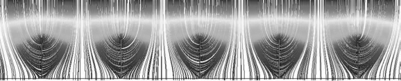
The device in Figure 17.2 shows a nanotube on the lower electrode and an upper electrode acting as an earth plane for the electric field. This upper electrode is made of transparent conducting material, indium tin oxide (ITO), on glass. A multi-wall carbon nanotube can be likened to a conductive metal rod of nanometer dimensions. When it is embedded between two plane electrodes in a sandwich structure, the nanotube changes the ideal plane electrostatic field profile. A theoretical study on the electrical field effects of carbon nanotubes has been carried out using the finite element method. A COMSOL finite element simulation of the electric field profile of the device structure, in Figure 17.2(a), is shown in Figure 17.3. The simulation assumes a conducting MWCNT in a vacuum and a good ohmic contact with the substrate underneath.
Figure 17.3 Simulated electrical field profile surrounding the single carbon nanotube (10 μm high) with an applied field of 1 Vm−1.
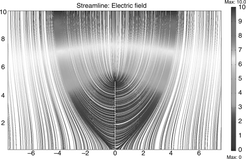
The ideal electrical field of a pair of parallel conducting plates is modified by the nanotube. The effective distance of the field from the nanotube is of the same order as the height of the CNT. The 2D model of a single nanotube has also been extended into 3D showing that the field profile is circularly symmetric about the centre of the nanotube. The curved electrical field profile in 3D can be used to control the behavior of the LC molecules as the field intensity is strong enough to reorient them with an applied field of 1 Vm−1. Varying the applied voltage changes the intensity of the field, the area over which the electric field extends, and hence the alignment of LCs within the area concerned. This makes the fabrication of a focus-tunable lens possible.
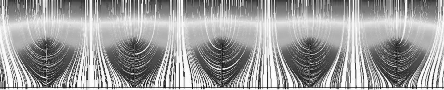
Figure 17.4 shows the 2D electrical field around a carbon nanotube array. Carbon nanotubes are spaced at a distance twice their height to minimize electrostatic field shielding from adjacent ones. Typical vertical multi-wall carbon nanotubes in arrays are 2–5 μm in height, which implies that the distance between two carbon nanotubes has to be at least 10 μm to ensure there is no electrostatic interaction between one another. This means that the LC micro lens array in a 10-by-10-mm chip would have a resolution of 1000 × 1000 lenslets for MWCNTs up to 5 μm high. For shorter MWCNTs, even greater density micro-optical arrays are possible. One of the main limitations of the microlenses formed in this structure is that they have a very tight aperture due to the localization of the electric field around the nanotube electrodes.
Figure 17.4 Simulated field profile of an array of nanotube electrodes at 1 Vm−1.
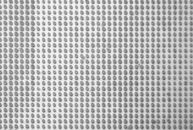
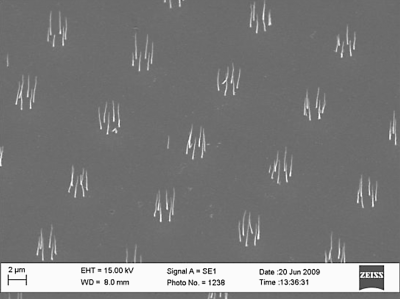
A typical array of individual nanotubes is shown in the electron microscope image of Figure 17.5(a) with a higher magnification view in Figure 17.5(b). In this case the nanotubes were patterned in small groups of 4 with 1 μm spacing between the nanotubes and 10 μm spacing between the groups.
Figure 17.5 Sparse array of nanotubes in groups of 4. (a) Array view with group spacing of 10 μm. (b) View of a single group with nanotube spacing or 1 μm.
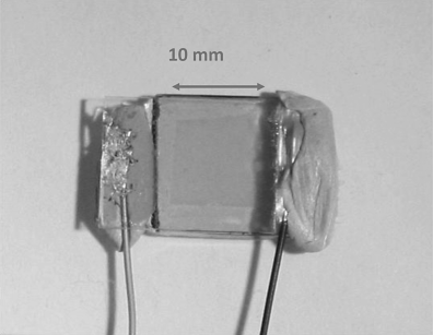
The sparse array in Figure 17.5 was then fabricated into a LC device. In order to make the device both reflective and also to provide a common electrical connection to all the nanotubes, 400 nm of aluminum was cold sputtered onto the array. The array was then assembled with a top electrode containing ITO on 0.5 mm thick borosilicate glass into a LC cell with a 20 μm cell gap set by spacer balls in UV glue. No alignment layer was applied to the nanotube array, but the top glass electrode was coated with AM4276 LC alignment layer and rubbed in the horizontal direction to give planar alignment. The cell was then capillary filled with BLO48 (positive dielectric anisotropy) nematic LC.
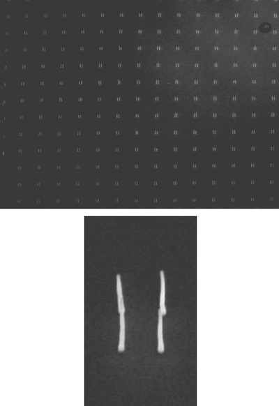
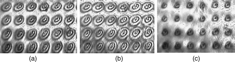
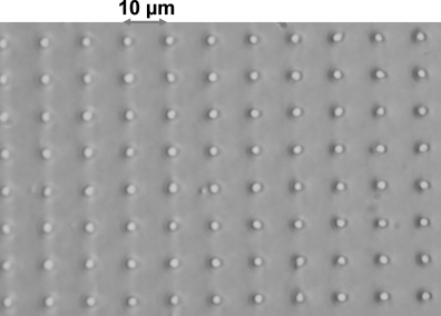
The assembled device was then viewed under horizontally polarized light on an optical microscope. The arrays of nanotubes were clearly visible as black dots as each 50 nm nanotube tip was the site for a defect in the nematic LC. Individual nanotubes with their groups of 4 could be seen at 40× magnification. Figure 17.6(a) shows the sparse array at zero applied electric field. The array of CNT groups can be clearly seen as defects in the image. As the applied field was increased, the nanotube electrodes were seen to begin switching at 1.8 Vm−1, which corresponds to the equivalent of a Freedrickzs transition. Figure 17.6(b) shows the nanotube array at 2.2 Vm−1 applied field and the nanotubes are now all fully switched. The distortion in the LC director can be seen in this image as visible contrast, with an analyzer in the horizontal direction, centred on each nanotube group. The irregular distortion structure seen in Figure 17.6(b) if not perfectly circularly symmetric due to the fact that the LC is horizontally aligned on the top substrate. The LC reorients to the field of the nanotube electrode in a complex manner, forming a twisted structure centered on each nanotube group.
Figure 17.6 Sparse nanotube array in a LC at 20× optical magnification under a polarizing microscope with the analyzer aligned parallel to the rubbing direction of the LC (horizontal). (a) 0 Vm−1 applied field, (b) 2.2 Vm−1 applied AC field.
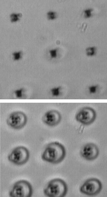
The distortion in the LC can also be seen without any polarizer or analyzer under the microscope as shown in Figure 17.7. Each feature is based around a group of 4 CNTs in the array and can be switched on and off with the applied electric field. Each feature resembles a roughly circular defect surrounding the CNT group.
Figure 17.7 Image of the LC–CNT array at 2.2 Vm−1 taken at 20× with no polarizer or analyzer on the microscope.
The lensing properties of these micro-optical elements were tested under the same microscope at 40×. Due to the limited depth of focus of the high magnification it should be possible to switch the CNT tip in and out of focus with an applied electric field. Figure 17.8(a) shows the array with 0 Vm−1 applied field and the microscope adjusted to be out of focus. The image in Figure 17.8(b) is the same area with an applied field of 2.1 Vm−1. The lensing function of the LC can be seen as the LC defect state at the tip of the nanotubes now appear in focus and are visible as a cluster of black dots at the centre of each lenslet.
Figure 17.8 Defocus of the nanotube lenslet array at 40×. (a) Defocused image of the array at 0 Vm−1 applied field. (b) Array brought into focus with 2.1 Vm−1 applied field.
17.8 Nanophotonic Device Characterization
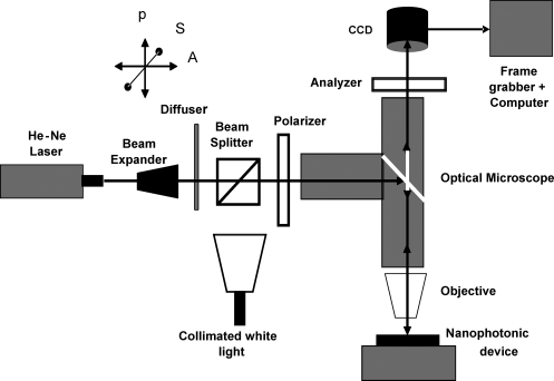
The microscopic phase profile of each lenslet is of interest as it decides the real modulation capability and applications of the device. The experimental set-up is shown in Figure 17.9. An optical microscope was used to detect the beam in reflective mode and for capturing the interference fringes. The setup consisted of a He–Ne laser along with a beam expander as the illuminating source. An objective having a magnification of 20× was used in the microscope. The device was mounted on a fine three axis tilting stage and attached to the microscope in reflective mode. The rubbing direction of the device was kept at 45° to the polarizer. The interference fringes were formed due to the interference between the ordinary and extra-ordinary beams being combined by an analyzer which was crossed with the polarizer [19]. A rotating diffuser (transparent plastic sheet) was used to average out speckle noise. The fringes were captured by a CCD camera and frame grabber. A white light source was used to see the device and to help in alignment. A voltage source was used to study the variation of interference fringes at different applied voltages. The interferogram, retrieved unwrapped phase profiles of an array of lenslet and one lenslet at different voltages are shown Figure 17.9.
Figure 17.9 Experimental set for recording interference fringes from the nanophotonic device in reflective mode.
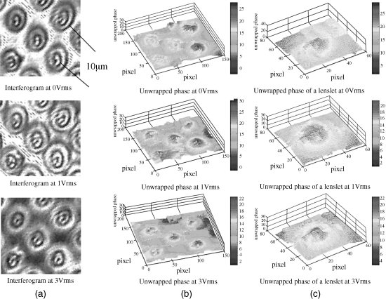
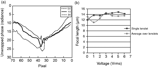
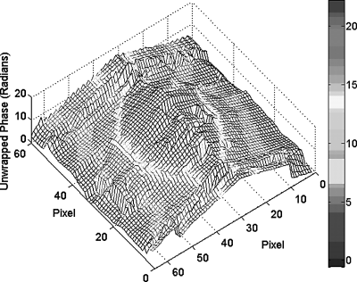
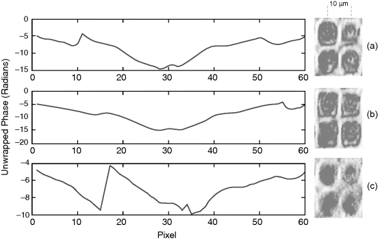
It was found that in the absence of an external voltage circular fringes were observed, which showed an alignment deformation of the LC molecules near the carbon nanotubes even though the macroscopic alignment was planar [Figure 17.10(a)]. The change in phase modulation (the phase difference between the center and circumference of each lenslet) was bigger at lower voltages than at higher voltages as shown in Figure 13.10 because the molecular alignment was more or less homeotropic at higher voltages. This resulted in a diminishing of the interference fringes. The phase profile was distorted at 0 Vrms, but became symmetric at 1 Vrms and distortion again started from 3 Vrms upwards for the device [20]. The focal length was calculated as follows
Figure 17.10 3D microscopic phase profile of an array at 0 Vrms, 1 Vrms and 3 Vrms (a) an array of interferograms, (b) unwrapped phase of the array, and (c) unwrapped phase of a lenslet.
where r is the radius of the lenslet, N the number of observed fringes and λ the wavelength of light. The above equation for the focal length can be written in terms of phase difference as
where OPD is the peak-to-valley optical path difference from the center to the edge, and r is the radius of the test area (5 μm). The variation in the focal length of a single lenslet and averaged over lenslets in a particular area of the device with respect to voltage is shown in Figure 17.11(b). The focal length of each lenslet at 0 Vrms is randomly varied. It was observed that the focal length increased with respect to the voltage and hence the lenslets were concave in nature. The focal length variation was in agreement with the simulation results (Figure 17.4), where the Gaussian profile gave maximum alignment at the centre of each lenslet compared to the circumference. An average focal length over the lenslets were calculated because, the focal length variation was found to be random after 3 Vrms for many lenslets and also a slight change in focal length between each lenslet below 3 Vrms in some areas of the device. The random behavior after 3 Vrms was because of the complicated electric field profile due to different ohmic contacts for each CNT.
Figure 17.11 (a) 2D unwrapped phase profile at 0 Vrms, 1 Vrms, and 3 Vrms; (b) focal length variation with respect to external voltage.
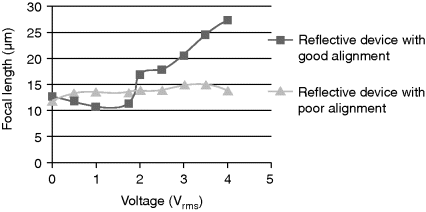
The phase profile of the device was also dependent on the alignment of the LC in the device. A device with better LC alignment gives more phase modulation than a device with poor alignment. Figure 17.12 shows the focal length variation of two devices with different alignment qualities. The focal length variation was from 11 μm to 15 μm for the voltage range 0 Vrms to 4 Vrms for a reflective device with poor alignment compared to 12–27 μm for a reflective device with good alignment.
Figure 17.12 Focal length variation with respect to external voltage for the devices with different alignments.
Reflective nano-photonic devices can be useful in display related applications such as when making high-resolution displays where each nanotube electrode addresses the LC molecules and hence the nanotube position acts as a single pixel. The advantage of the silicon device is that electronics can be easily integrated with the silicon using standard silicon fabrication technologies. Another application is displaying complicated holograms for 3D displays and as an electrically reconfigurable optical diffuser. Optical diffusers change the angular divergence of incident light as well as act as a random phase modulator. The current device acts as a grating at the same time because of the periodically arranged CNTs with 10 μm separation and microlensing due to the LC graded index. The device can be used for homogenous illumination that is reconfigurable with an external voltage. The device has over 106 lenslets within the 10 mm2 area. From a geometric optics perspective, the greater the number of elements in the lens array, the finer the separation of the incident beam and hence the more uniform the illumination [21]. The lenslets in the device are not completely identical in performance, which helps to suppress multiple beam interference patterns due to the spots generated by each lenslet. This can further enhance the uniformity of illumination.
17.9 Carbon Nanotube Electrode Optimization in the Device
In order to find out a suitable nanotube electrode geometry in the nanophotonic device, the electrode number, and geometry was varied mainly from one, three, four, and five. The period of the nanotubes group was kept at 10 μm and separation between each nanotube at 1 μm. All other parameters such as thickness of the cell and alignment were also kept constant for all the device geometries. The results were obtained from both electric field simulations and experimentally.
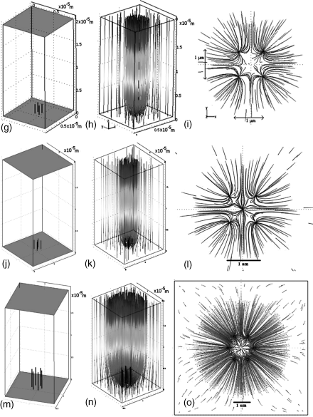
The resultant electric field widens as the number of nanotubes per group increases. For device applications, the resultant electric field needs not only to be wide but also symmetric. The number of nanotubes and separation between each nanotube in a group decided the symmetry of the resultant electric field. The electrostatic simulations were carried out by varying the number and geometries of the nanotube electrodes per group. Figure 17.13 shows the electric field profile generated by one, three, four, and five nanotubes per group with each nanotube separated by 1 μm. The group was repeated at 10 μm intervals. It was clear from the simulation that one nanotube electrode generated a symmetric field profile. But the resultant field was narrower than the other geometries. The three nanotube group electric field profile was not symmetric compared to all other geometries. Four and five nanotubes generated wider resultant electric field profiles than the other geometries. By considering the symmetry and minimum number of nanotubes per group, four nanotubes was found to be most suitable for micro-lens applications. The higher numbers of nanotubes per group were also considered such as six and eight. The six nanotube geometry is also suitable for micro-lens array applications with wider lenslet apertures as shown in Figure 17.14. Figures 17.15 and 17.16 show the 3D resultant electric field simulation for one, three, four, five, and six nanotubes groups. The simulation results were experimentally verified by fabricating devices with some of the different geometries.
Figure 17.13 Modeled 2D electric field profile produced by a group of one, three, four, and five carbon nanotubes placed 1 μm apart.
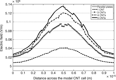
Figure 17.14 Modeled 2D electric field profile produced by a group of six nanotubes.
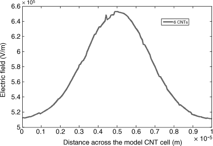
Figure 17.15 3D models for the groups of (a) one nanotube and (d) three nanotubes, in free space, connected 1 μm apart. Streamline view of the simulated E Fields generated by the groups of (b) one nanotube and (e) three nanotubes. (c) and (f) present the same in the x–y plane, respectively. The direction of E-Field lines indicates the repulsion present due to neighboring nanotubes.
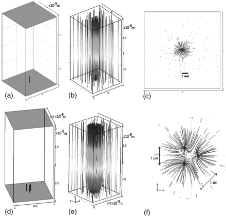
Figure 17.16 3D models for the groups of (g) four nanotubes, (j) five nanotubes, and (m) six nanotubes, in free space, connected 1 μm apart. Streamline view of the simulated E fields generated by the groups of (h) four nanotubes, (k) five nanotubes, and (n) six nanotubes. (i), (l), and (o) present the same in the x–y plane, respectively. The direction of E-field lines indicates the repulsion present due to neighboring nanotubes.
17.10 Carbon Nanotube Electrode Optimization: Experimental Results
Based on the simulation results, devices with different number of nanotubes and geometries were fabricated such as one, three, four, and five. The experimental results matched the electric field simulations. The phase profile of each nanotube element (lenslet) was recovered to study refractive index profile, resultant phase modulation capabilities and focal length variation of the device.
Figure 17.17 shows SEM picture of an array of single nanotube electrodes on silicon substrate. The electrodes were separated by 10 μm. The height of the nanotube electrode was around 4–6 μm. The device was fabricated using a planar alignment on the top electrode as discussed in the previous sections.
Figure 17.17 Scanning electron microscope (SEM) image of single nanotube electrode on silicon substrate.
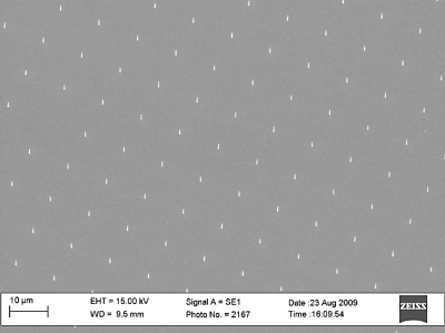
Figure 17.18 shows interference fringes recorded from the device at different applied voltages using the interference setup shown in Figure 17.9. It was found that fringes were observed at 0 Vrms because the nanotube distorted the planar alignment of the LC molecules around it. The fringes were symmetric and wide at around 1.3 Vrms. The fringes disappeared as the voltage increased above 3 Vrms. This is because the LC molecules aligned almost homeotropically at higher voltages. Figure 17.19 shows the unwrapped phase profile of one lenslet. The unwrapped phase became symmetric and wider at around 1.3 Vrms and distorted as the voltage increased. The maximum phase modulation observed was 4π. The one nanotube electrode geometry gives a symmetrical phase profile and is suitable for lens array applications. However, the field profile is narrow which results in small diameter lenslets and hence the lensing is weak. But the single nanotube electrodes are suitable for high-resolution display applications where each nanotube site acts as a pixel with minimum fringing field effects.
Figure 17.18 Interference fringes at different voltages from one nanotube device. (a) 0 Vrms, (b) 1.3 Vrms, and (c) 3.5 Vrms.
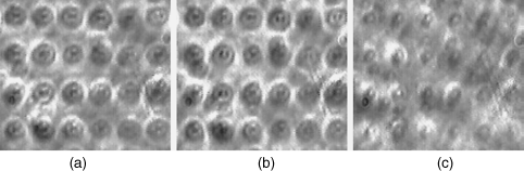
Figure 17.19 Unwrapped phase of a one nanotube lenslet at 1.3 Vrms.
Three nanotube electrodes were grown on silicon substrate as shown in Figure 17.20. Each nanotube was separated by 1 μm in the group and the group repeated in 10 μm. The fabrication method was same as in Section 7.
Figure 17.20 SEM image of three nanotubes electrode on silicon substrate.
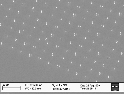
Figure 17.21 shows the interference fringes obtained from the device using an interference setup. It was clear from the interferogram that the fringes are asymmetric and distorted. The unwrapped phase profile was recovered to understand the phase modulation and symmetry in detail. The lenslet diameter increased with voltage and there was more overlapping between lenslets at around 1.3 Vrms. Three nanotubes electrode was not best suited for lensing applications as the interference fringes were not circular and phase profile distorted.
Figure 17.21 Interference fringes at different voltages from 3CNT device. (a) 0 Vrms, (b) 1.3 Vrms, and (c) 3.5 Vrms.

Figure 17.22 shows SEM picture of a four nanotubes electrode on the silicon substrate. All other device parameters were same as the previous devices. Figure 13.22 shows interference fringes from the device at different applied voltages such as 0 Vrms, 1.3 Vrms, and 3 Vrms. The fringes were wider at around 1 Vrms with maximum phase modulation capability as shown in Figure 17.23. The fringes disappeared at higher voltages as discussed for the previous geometries. The unwrapped phase became almost symmetric and widest at around 1 Vrms and distorted as the voltage increased. The four nanotubes electrode geometry gave an almost symmetrical phase profile with wide resultant field and was suitable for a lens array.
Figure 17.22 SEM image of four nanotubes electrode on silicon substrate.
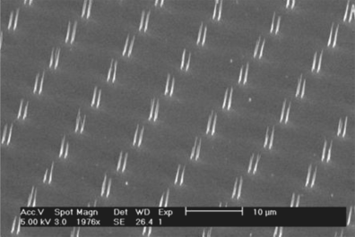
Figure 17.23 Interference fringes at different voltages from 3CNT device. (a) 0 Vrms, (b) 1.3 Vrms, and (c) 3.5 Vrms.
Five nanotube electrodes were grown on silicon substrate as shown in Figure 17.24. The fabrication parameters were same as the previous devices.
Figure 17.24 SEM image of five nanotube electrodes on a silicon substrate.
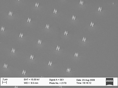
Figure 17.25 shows interference fringes recovered from the device at different applied voltages. The fringes are almost symmetrical with a small distortion at the center of the fringes. This is due to the centre nanotube in the five group distorting the refractive index profile and gradient at the center of each lenslet. This was further studied by recovering the unwrapped phase from the fringes. The lenslet phase profile was distorted. Though the fringes were almost symmetrical for the five nanotube geometry, there was distortion at the centre of each lenslet and was not suitable for lens array applications.
Figure 17.25 Interference fringes at different voltages from 5CNT device. (a) 0 Vrms, (b) 1.3 Vrms, and (c) 3.5 Vrms.
17.11 Transparent Nanophotonic Device
The nanophotonic devices discussed so far operate in a reflective mode [8]. The reflective devices were fabricated on silicon substrate and were made reflective by providing a thin layer of aluminum on the silicon which also acted as a common electrode. Such devices are useful for display applications or for displaying complicated 3D holograms because electronics could easily be integrated with the silicon. In this section, characteristics of the transparent nanophotonic device are presented. The transparent nanophotonic device was fabricated on a quartz substrate and covered with nematic LC to give light modulation capabilities [30]. The device has proven ideal for making voltage dependent high resolution nanophotonic lens arrays, a wave front sensor, diffuser and grating. Figure 17.26 shows a transparent nanophotonic device where nanotubes are grown vertically on the lower electrode and an upper electrode is acting as an earth plane for the electric field. The lower electrode was made from a quartz substrate with a 100-nm thick titanium nitride layer for an electric contact and the upper electrode with ITO on 0.5-mm thick borosilicate glass. The cell gap was set at 20 μm using spacer balls in UV glue and was filled with a nematic liquid, BL048 from Merck. The top electrode alone was given a planar alignment layer by rubbing a thin film of polyimide (AM4276) and hence the resultant alignment of the device was hybrid.
Figure 17.26 Carbon nanotube and LC-based transparent nanophotonic device.
In the current device, the nanotubes were patterned in small groups of six with a 1-μm spacing between the nanotubes and a 10 μm spacing between the groups to increase the resultant electric field and hence the diameter of each phase modulating element as shown in Figure 17.27.
Figure 17.27 Electron microscope image of multi-wall carbon nanotube electrodes on a quartz substrate.
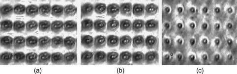
The transparent device was viewed under a polarized optical microscope in transmission mode at different voltages. The device started switching at 0.75 Vrms, which corresponds to the equivalent of a Freedrickzs transition. The light focused at each nanotube site (lenslet) of the device was clearly visible when viewed under the microscope. Figure 17.28 shows the device switching at 1.1 Vrms.
Figure 17.28 The transparent device at 1.1 Vrms under optical microscope (50× magnification).
The phase modulating capabilities of the transparent device were studied at different voltages experimentally. The set-up consisted of a He–Ne laser along with a beam expander as the illuminating source similar to that in Figure 17.9. An optical microscope was used to detect the beam in transmission mode and for capturing the image. An eyepiece having a magnification of 20× was used in the microscope. The device was mounted on a fine three-axis tilting stage and attached to the microscope in transmission mode. The rubbing direction of the device was kept at 45° to the polarizer. The interference fringes were formed owing to the interference between the ordinary and extraordinary beams being combined by an analyzer that was crossed with the polarizer [19]. A rotating diffuser (transparent plastic sheet) was also used to average out speckle noise. The fringes were captured by a CCD camera and frame grabber. A voltage source was used to study the variation of interference fringes at different applied voltages. The interferogram of four lenslets and retrieved unwrapped phase profile of one lenslet at 0 Vrms, 1.1 Vrms, and 6 Vrms of the transparent device with a six-nanotube group with each nanotube separated by 1 μm and a period of 10 μm are shown in Figure 17.29. The fringes were observed at 0 Vrms due to the alignment of the LC molecules by the carbon nanotubes even though the top electrode was given a planar alignment. The interference fringes were more or less circular and clear at lower voltages. As the voltage increased, the circular fringes became rectangular in shape due to repulsion of electric field from each of the carbon nanotube groups. The fringes started to disappear at around 2.5 Vrms and a black spot was observed at the position of each lenslet. The phase modulation was 2.86π at 0.98 Vrms with distorted phase profile. The phase profile became smooth and parabolic at voltages below 2 Vrms with phase modulation of 3π–4.2π. The phase modulation decreased with the distortion in phase profile as the voltage increased.
Figure 17.29 Unwrapped phase of a single lenlet and interference fringes from the nanophotonic device (four lenslets) at 0.98 Vrms. (a) 1.1 Vrms and (b) 2.5 Vrms.
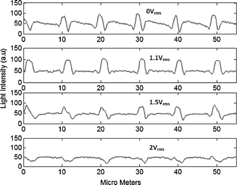
Light intensity and focal length variation of the device at each nanotube group site (lenslet) were studied to understand the imaging characteristics of the device. These parameters are also needed for making suitable applications using the device. In order to study the light intensity profile from each lenslet, the device was fixed in a polarized microscope where the objective was focused on to the top of each nanotube position. The image of the device was recorded on a CCD at different voltages. The light focusing effect at different voltages is shown in Figure 17.30(a)–(f). The nanotubes distort the planar orientation of the LC around the nanotube which results in a graded refractive index profile. At 0 Vrms, the light focusing was not uniform for all the lenslets because the LC distortion was different for each nanotube position as shown in Figure 17.30(a). The focusing started improving as the voltage increased from 0 Vrms. The light focusing at 0.75 Vrms is shown in Figure 17.30(b). The focusing of light became most uniform at around 1.1 Vrms and light intensity increased at each lenslet position as shown in Figure 17.30(c). The focusing effect reduced with further increase in the applied voltage. This can be seen in the images at 1.8 Vrms and 2 Vrms, as shown in Figures 17.30(d) and (e), respectively. As the voltage increased above 2 Vrms, the light intensity at each lenslet position started decreasing and finely disappeared at higher voltages as shown in Figure 17.30(f). Figure 17.31 shows one-dimensional (1D) cross section of the intensity profile across five lenslets at 0, 1.1, 2.2, and 3 Vrms. It was clear that at 0 Vrms the light intensity was more at the nanotube positions compared to that remaining in the area of the device. But the light intensity between each of the nanotube groups was not uniform and hence created an aberrated lens array. When the voltage was 1.1 Vrms, the light intensity was maximum at these nanotube positions with a wider profile. The light intensity was also smooth and uniform between the nanotube groups. The device acted as a lens array with least aberration at around 1.1 Vrms. Further increase in the voltage distorted the light intensity profile and there was no proper lensing above 1.8 Vrms.
Figure 17.30 The nanophotonic lens array focusing the light at (a) 0 Vrms, (b) 0.75 Vrms, (c) 1.1 Vrms, (d) 1.8 Vrms, (e) 2 Vrms, and (f) 4 Vrms.
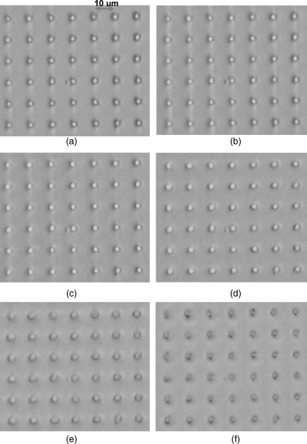
Figure 17.31 The 1D light intensity profile across six lenslets at (a) 0 Vrms, (b) 1.1 Vrms, (c) 1.5 Vrms, and (d) 2 Vrms.
The focal length of each lenslet was calculated using the Eqs (17.3) and (17.4). The focal length varied with respect to the applied voltage as shown in Figure 17.32. Further increase in the voltage distorted the orientation of the LC molecules in the device and hence no focusing was observed. The nanophotonic device was, however, acting like a voltage reconfigurable lens array at lower voltages. The focal length variation was due to the change in phase profile with respect to the applied voltage. The focal length varied from 10 μm (0 Vrms) to 36 μm (2.2 Vrms) and hence the lens array became more concave in nature with increased applied voltage. The lensing nature of the lens arrays disappeared after 3 Vrms because the LC molecules aligned randomly at higher electric fields. The focal length variation was slightly better for the transparent sample because the light was incident normal to the device surface and there was no double pass of light through each micro lenslet as in the case of the reflective device. Only the transparent device can be used for imaging applications because of the easy integration with rest of the optical components and lower distortion in the image.
Figure 17.32 Focal length variation of one lenslet with respect to applied voltage. Region ‘A’ represents the useful region for imaging.
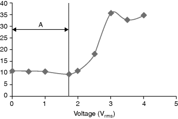
The light intensity variation across the lenslet in the device and focal length variation with respect to the applied field was calculated to find the useful range for imaging applications. Though the focal length varied from 10 μm to 36 μm, the useful region for imaging was found to be from 10 μm to 14 μm which corresponds to the voltage range 0–1.8 Vrms. There were distorted interference fringes above 1.84 Vrms and hence the focal length variation.
From the light intensity studies it was clear that the light focusing ability of the device considerably decreased from 1.8 Vrms upwards. This was due to the fact that as the voltage increased above 1.8 Vrms, the alignment of LC molecules got distorted and further increased in the voltage forced the molecules at each nanotube site to align homeotropically. Figure 13.32 shows the focal length verses voltage graph where the region ‘A’ is most useful for imaging. The focal length varied until 4 Vrms because the interference fringes were present up till this voltage. The number of fringes decreased as the voltage increased above 1.8 Vrms.
17.12 Nanophotonic Compound Eye-Based 3D Vision Sensor
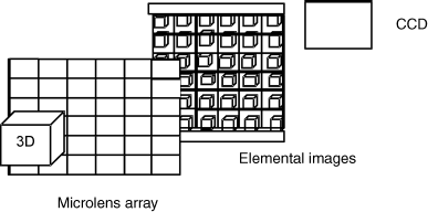
Large vertabrates like humans have large single aperture eyes. The eyes are optimized to provide high resolution, large field of view, focusing ability, color detection, and a very large dynamic range to see both in the bright sunshine and in the dark night. Small invertebrates on the other hand cannot afford large single heavy aperture eyes that consume a lot of metabolic energy. They have instead compound eyes, where the image capturing is distributed amongst a matrix of small eye sensors. Miniaturized imaging systems based on artificial compound-eye vision have been examined experimentally by several groups [22, 23]. Little attention has been paid to the optical imaging system compared to the comparatively large effort in the electronics, and the burden of the extraordinarily complex image processing. This has prevented the realization of a fully functional, miniaturized high-resolution compact camera. Their optical performance has also been limited by inadequate fabrication and assembly technologies for the individual components. This chapter presents the development of a nanophotonic 3D sensor system for high resolution 2D imaging, and 3D video by overcoming the diffraction barrier. The key component for achieving this goal is the imaging optics itself. We have developed a novel nanophotonic micro-lens array as discussed in Chapter 4 suitable for a compound eye based high-resolution imaging sensor. We apply integral imaging to enable 3D video/display in the sensor to give advantages such as continuous view points, full parallax, no convergence-accommodation conflict and no need for any special glass to evoke the 3D image.
Integral imaging is based on integral photography, which was proposed by Lippmann [24]. Integral imaging is a 3D image display technique that produces true 3D images. The advantages of integral imaging compared to other 3D image systems include continuous view points, full parallax, no convergence accommodation conflict and no special viewing glasses are required to see the 3D image [25–28]. It is an auto stereoscopic technique where the 3D object is sampled by a micro-lens array or a pinhole. Each micro lenslet picks up a particular perspective of the object which is called an elemental image. Reconstruction of a 3D image of the object from 2D elemental images is a reverse of the pickup process. The 3D image is reconstructed from all the elemental images using a lens array.
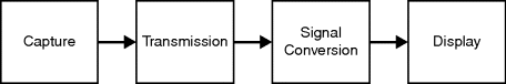
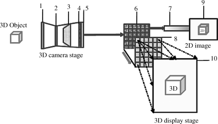
Figure 17.33 shows the block diagram of the camera and display stage. The camera stage is the capture stage. The captured image is transmitted as electrical signals and converted back into optical signal in the display stage.
Figure 17.33 Block diagram of camera (pick up) and display stage.
The integral imaging system can be divided into camera stage (pick up stage) and display stage (3D image reconstruction stage). Figure 17.34 shows the principle of the pickup method by a camera. The 3D object is sampled by a micro-lens array. An inverted real image (for a convex lens array) of the object is created by each micro lenslet behind the micro-lens array. The image formed by each lenslet is called the elemental image. Each elemental image is formed from a different perspective of the object. Then all the elemental images are recorded on a CCD camera.
Figure 17.34 Block diagram of the camera stage.
We define the following parameters, WL is the width of the lens array, WS is the width of the pickup device, fC is the focal length of the camera lens in front of CCD to demagnify all the elemental images down to the size of the CCD, and ![]() is the distance between the lens array and the camera lens [27].
is the distance between the lens array and the camera lens [27].
(17.5) ![]()
(17.6) ![]()
Also WM is the pitch of the microlenses, N is the number of micro lenslets, M is the number of pixels in the elemental image, and PC is the pitch of the pickup device. It is clear from the above equations that the number of pixels in the pickup device is the product of the number of micro lenses and pixels in the elemental image. The resolution of the reconstructed 3D image is given by the number of micro lenses. The number of pixels per elemental image is related to the viewing zone, or the resolution, of the reconstructed 3D image. It has been experimentally observed that at least ten pixels per elemental image in the vertical and horizontal directions are required for minimum clarity in the reconstructed 3D image.
The 3D image can be reconstructed from the elemental images by two methods, namely computational reconstruction or optical reconstruction. Computational reconstruction uses pixel mapping techniques to get 3D/2D image. In optical reconstruction, the reconstruction is done using a LCD and lens array in real time, and is useful for 3D video and microscopy. Real time or computational 2D reconstruction of the image from the elemental images is used for compound eye-based imaging systems. Integral imaging technique provides a 3D image from the elemental images and that aspect is explored further in this chapter.
17.13 Optical Reconstruction Technique
In the optical reconstruction stage, the set of elemental images is displayed on a LCD in front of a second lens array [28, 29]. The light rays from these elemental images then go through the lens array, reconstructing the image of the object at the same position as the object as shown in Figure 17.35. Note that although all the elemental images are imaged by the corresponding lenslet into the same plane or the reference image plane, the 3D scene is reconstructed in the image space by the intersection of the ray bundles emanating from each of the lenslets. This method allows viewers to observe a reconstructed 3D image in real time floating in air. Here also the resolution of the reconstructed 3D image is given by the number of lenslets in the lens array. The viewing angle and the depth of the reproduced 3D images depend on the focal length of the convex lenses. The viewing angle Φ is expressed as [28]
Figure 17.35 Schematic diagram of the proposed 3D vision sensor. 1 – imaging lens, 2 – nanophotonic lens array, 3 – pinhole array (optional), 4 – CMOS/CCD sensor, 5 – control electronics, 6 – LCD, 7 – pixel mapping/image processing, 8 – large lens array, 9 – out put 3D image, 10 – output: 2D image (compound eye sensor).
(17.7) ![]()
where P is the pitch of the elemental image and g is the distance between the principle plane and elemental images on the LCD.
The main resolution limitation of this 3D imaging sensor lies in the resolution of the micro-lens array. Miniaturization strategies that have been applied with great success to electronics cannot be simply transferred to optical imaging systems. We have started to exploit nanophotonics and integral imaging technologies to overcome these issues. In the designed sensor, the above mentioned problems of imaging optics, resolution, and miniaturization issues of the sensor system are addressed by introducing the transparent nanophotonic lens array, where each lenslet radius is of the order of 5 μm which is much smaller compared to any commercially available fixed lens array and the focal length is voltage reconfigurable. Applications of this type sensor are mainly in miniaturized 3D camera, 3D microscopy, and endoscopy. Figure 13.35 shows the general architecture of the sensor.
The sensor head (camera stage) has an imaging lens (convex lens). The imaging lens is used to demagnify the image of a far away object to a suitable scale. The voltage dependant lenses also give us an option to get real and virtual 3D image capture by changing the focal length. Without this lens the operating distance of the sensor is limited to millimeters and field of view is very small. When multiple objects are present at a large distance, without this imaging lens only nearby objects get clarity in the image plane and other images will be out of focus. The 3D images near the lens array for reproduction have a higher resolution than those farther away from the lens array. These problems can be solved by incorporating a suitable imaging lens. The imaging lens focuses the image in front (for real 3D) or behind (for virtual 3D) of the nanophotonic micro-lens array to generate many elemental images. The elemental images are recorded on a high resolution CCD/CMOS recording device.
The display stage has a high-resolution LCD where all the elemental images recorded by the CCD are displayed. The large lens array to reconstruct the 3D image was fabricated from crossed lenticular sheet with 10 lines per in inch (10 LPI). In the lenticular lens array, two lenticular sheets (10 LPI acrylic sheets with refractive index 1.49) were crossed at right angles. The lens side of the two lenticular sheets was contacted together in this scheme. Since the focal length of the lens is determined only by the lens side, the two lens arrays have the same focal length when crossed at right angle. The fabricated lens array is shown in Figure 13.36. The light focusing capability of the lens array was studied using a white light source. The lens array focused light in the back focal plane as shown in Figure 17.36. The focal length of the array was experimentally measured at 3.9 mm from the center of the lens array.
Figure 17.36 Left, lens array fabricated from two lenticular sheets having pitch 2.5 mm; right, light focused by the lenticular lens array.
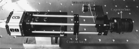
Calibration of the 3D vision sensor was performed using a standard micro-lens array (suss micro-optics, circular lenses, quadratic grid: lens pitch 110 μm, ROC 0.817 mm, numerical aperture 0.03, size 15 mm × 15 mm × 0.9 mm) in the camera stage to fix system parameters. Figure 17.37 shows the 3D vision sensor camera stage developed for calibrating the system parameters including the display stage and the lens array fabricated with two lenticular sheets. The sensor consists of capture lens (imaging lens) to demagnify the image of a far away object to a suitable scale followed by the standard micro-lens array to sample the image and CCD with a convex lens to record the elemental images. We used a very high resolution CMOS color camera (EO-10012C ½ inch CMOS Color GigE) to record the elemental images with pixel resolution 3840 × 2748 and pixel size 1.67 × 1.67 μm in the camera stage.
Figure 17.37 The 3D vision sensor camera stage developed. (See the color version of this figure in Color Plates section.)
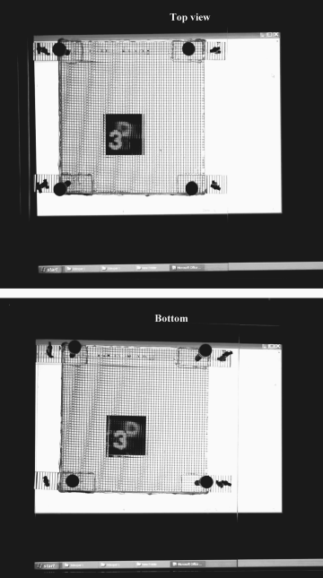
The 3D display stage for the sensor was fabricated using the crossed lenticular lens array and silicon graphics 1600SW, 17 in. LCD monitor as shown in Figure 13.38. The dot pitch of the display was 0.23 mm for high resolution. The separation between the display and the lens array was adjustable for improving the quality of the 3D image reconstructed. The size of the lens array was 15 × 15 cm. Computationally simulated elemental images of the number 3D was used to calibrate [29] the display as shown in Figure 17.38. The inverted version of the image was used in experiment. All the elemental images were displayed on the display and the lenticular lens array was kept 4 mm away (the distance measured from centre of the lens array to the display). Figure 17.39 shows the reconstructed 3D image in the display from two different angles (top view and bottom view). The ‘D’ moved with respect to the ‘3’ in top and bottom view. This shows that there was a full parallax in the reconstructed 3D image. Each elemental images was displayed using 10 × 10 pixels on the LCD and each elemental was covered by a single lenslet of size 2.5 mm on the lenticular lens array. This experiment helped to fix the distance between the lenticular lens array and the display stage.
Figure 17.38 Fabricated 3D display stage using crossed lenticular lens array and silicon graphics 1600 SW, 17 in. LCD monitor, the elemental images of 3&D [29].
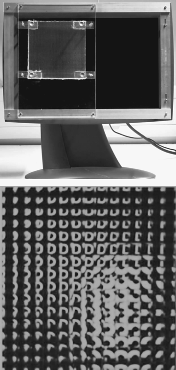
Figure 17.39 The reconstructed 3D image in the developed 3D display from all the elemental images viewed from top and bottom. (See the color version of this figure in Color Plates section.)
17.14 Imaging Using the Nanophotonic Lens Array
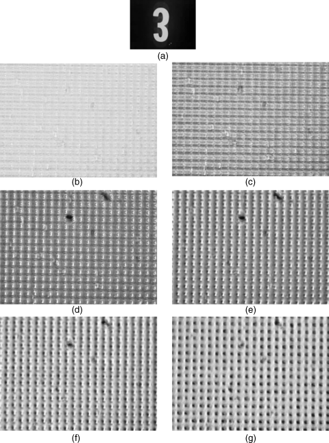
The imaging characteristics of the nanophotonic lens array were studied for calibration. US air force (USAF) test pattern was used an object. A transmission microscope with a CCD camera was used to capture the images from the nanophotonic device at different voltages. The number 3 (100 μm) in the USAF pattern was used for imaging.
The images formed from the nanophotonic lens array was not clear at zero volts because of the less ordered alignment of the LC molecules around the nanotubes and hence created a non uniform gradient refractive index profile. This matched the interference experiments where fringes were observed at zero volts as discussed in Section 8. The images became very clear at 1.1 Vrms and started disappearing with increase in the applied voltage. The performance exactly matched with the focal length study. Figure 17.40 shows the image formed from the nanophotonic lens array at different voltages.
Figure 17.40 Object used and captured elemental images from the nanophotonic lens array at different voltages (a) object, (b) images at 0 Vrms, (c) images at 0.75 Vrms, (d) images at 1.1 Vrms, (e) images at 1.8 Vrms, (f) images at 2.2 Vrms, and (g) images at 3.5 Vrms.
The focal length variation and the phase profile with respect to the applied voltage of the nanophotonic lens array were as discussed previously. The focal length increased with respect to the applied voltage and hence the concave nature increased. The behavior of the lens array at 0 Vrms and close to 0 Vrms was not clear from the previous results. The image formation at various distances from the nanophotonic lens array was used to find the behavior of the lens array at 0 Vrms. Figure 17.41 shows the images captured of the object ‘3’ at different images planes. In Figure 17.41(b), the image plane was 10 μm away from the plane at Figure 17.41(a).
Figure 17.41 The images formed at two different focal planes (b) the focal plane is 10 μm away from the image focal plane (a).
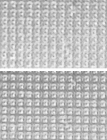
It was clear from the images that the image size reduced with distance as well as the fact that the images were non-inverted and hence both planes were before the focal plane. When the distance increased by another 30 μm from the previous plane, the focal plane was reached as shown in Figure 17.42. When the distance increased by another 41 μm from the focal plane, the inverted images appeared and hence the image plane was after the focal plane as shown in Figure 17.43(a). With a further increase in distance of 5 μm, the image size increased as shown in Figure 17.43(b). Hence the refractive index profile created a distorted convex lens at 0 Vrms and the convex nature reduced (concave nature increased) with respect to the applied voltage. In some part of the lens array, the convex nature slightly increased at very lower voltages just after 0 Vrms and then concave nature increased with further increase in voltage. The nanophotonic lens array is useful for imaging just before the concave nature increases. This is because when the concave nature increases, there is more distortion in the refractive index profile. The optimum voltage for the imaging was around 1.1 Vrms.
Figure 17.42 An image plane near to the focal plane.
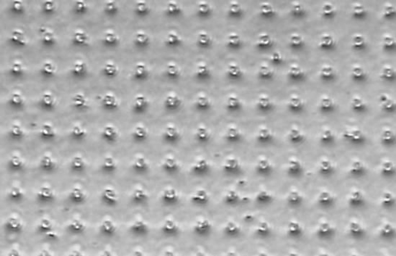
Figure 17.43 The images formed at two different focal planes (b) the focal plane is 5 μm away from the image focal plane (a).
17.15 Conclusions and Discussion
In this chapter we have presented a nanophotonic device based on a hybrid combination of multi-wall carbon nanotubes and LCs. The carbon nanotube electrode arrays were grown on silicon substrate (reflective device) and on quartz (transparent device) by plasma enhanced chemical vapor deposition after employing e-beam lithography and covered with nematic LC. The multi-wall carbon nanotubes act as individual electrode sites that spawn an electric-field profile, dictating the refractive index profile within the LC and hence creating a series of graded index profiles, which form various photonic elements. The device was analyzed under an optical microscope and it was found that photonic element was formed at each nanotube site and the photonic elements switched with respect to the applied voltage. This has led to the conclusion that micro/nano regions in the device interact with light.
The phase profile from micro region in the device was recovered using an interference set-up attached with an optical microscope. Each nanotube site acted like a lenslet. The phase profile was more or less parabolic at lower voltages and hence acted like a voltage reconfigurable nanophotonic lens array. The effect of nanotube electrode geometry in the phase profile and the lenslet diameter has been studied using electric field simulation followed by fabricating the devices with one, three, four, and five nanotube groups. The four nanotube group was found to be optimum for lens array applications and one nanotube for display applications. However, a larger number of nanotubes per group could be used for increasing the lenslet diameter.
A transparent nanophotonic device was also discussed where the nanotube electrodes were grown on a quartz substrate. The device is suitable for lens array applications because of the easy alignment with other optical components and there was no double pass of light through the device. The electrode geometry used had six nanotubes per group in a hexagonal pattern. The phase profile and focal length were calculated and found that the device acted as nanophotonic lens array at lower voltages. The light focusing was also studied at different voltages to understand the focusing properties of the device. The light intensity profile at each lenslet was smooth and maximum at a lower voltage and at the same voltage the phase profile was parabolic like. The useful voltage range of the device for imaging application was obtained from the studies of phase profile, phase aberrations, intensity profile, and focal length variation. Electro-optic characteristics, such as transmission voltage characteristic, response time and the contrast ratio of the device were studied to optimize the device performance for different applications. These analyses showed that the device finds application as a nanophotonic lens array, reconfigurable hologram, and grating at lower voltages in addition to the suitability of the device for display application at higher voltages.
This chapter also presented a 3D vision sensor realized using the nanophotonic lens array. The imaging characteristic of the lens array was studied using USAF test pattern at different voltages. The useful voltage range for imaging obtained from the imaging experiments were matched with previously obtained voltage range from the intensity profile. An insect eye-based imaging system was developed first where each nanophotonic lenslet captured a particular perspective of an object called the elemental image. The number of elemental images was equal to number of lenslets. One pixel from each elemental image was extracted to get a 2D image of the object as in the case of compound eye imaging system of an insect. This imaging system was then extended using integral imaging techniques to realize a 3D vision sensor. The pick up stage (camera stage) and display stage were developed and integrated together. The 3D sensor was then calibrated using a standard micro-lens lens array, plastic objects and simulated elemental images. The sensor was also modified into a 3D microscope for analyzing microscopic objects. Since the focal length of the nanophotonic lens array was in micro meters range, the elemental images formed was just before the diffraction effect predominated and hence over came the limitation imposed by diffraction. The concept of the 3D microscope can be extended to realize a 3D endoscope where the image floats in the air with full parallax. The advantage of the current technique is that it can give very high resolution of the specimen under observation and the endoscope can be realized in a small foot print. Another advantage is that the 3D image can be seen without any glasses to many viewers with full parallax.
The potential applications of this type of nanophotonic device range from 3D cameras through to wavefront sensors. Furthermore other structures can be made using the ebeam patterning system to locate the CNTs from holograms and gratings [31] through to photonic bandgap metamaterials [32]. The spacing of the tubes can be set down to 500 nm as has been recently demonstrated in work on CNT-based metamaterials [33]. By controlling lattice structures and defects, filters, lenses, and waveguides can all be fabricated using these principles. Their operation can then be further enhanced with the inclusion of a variable refractive index material such as a LC into these novel 3D nano-structures.
1. F. S. Yeung, J. Y. Ho, Y. W. Li, F. C. Xie, O. K. Tsui, P. Sheng, and H. S. Kwok. Variable liquid crystal pretilt angles by nanostructured surfaces. Appl. Phys. Lett. 2004, 85, 513.
2. J. T. K. Wan, O. K. C. Tsui, H.-S. Kwok, and P. Sheng. Liquid crystal pretilt control by inhomogeneous surfaces. Phys. Rev. E 2005, 72, 021711.
3. O. Trushkevych, N. Collings, T. Hasan, V. Scardaci, A. C. Ferrari, T. D. Wilkinson, W. A. Crossland, W. I. Milne, J. Geng, B. F. G. Johnson, and S. Macaulay. Characterization of carbon nanotube–thermotropic nematic liquid crystal composites. J. Phys. D: Appl. Phys. 2008, 41, 125106.
4. S. J. Jeong, P. Sureshkumar, K.-U. Jeong, A. K. Srivastava, S. H. Lee, S. H. Jeong, Y. H. Lee, R. Lu, and S.-T. Wu. Unusual double four-lobe textures generated by the motion of carbon nanotubes in a nematic liquid crystal. Opt. Exp. 2007, 15, 11698–11705.
5. I.-S. Baik, S. Y. Jeon, S. J. Jeong, S. H. Lee, K. H. An, S. H. Jeong, and Y. H. Leeb. Local deformation of liquid crystal director induced by translational motion of carbon nanotubes under in-plane field. Jpn. J. Appl. Phys. 2006, 100, 074306-1-5.
6. C.-Y. Huang, C.-Y. Hu, H.-C. Pan, and K.-Y. Lo. Electrooptical responses of carbon nanotube-doped liquid crystal devices. Jpn. J. Appl. Phys. 2005, 44, 8077–8081.
7. W. Lee, C.-Y. Wang, and Y.-C. Shih. Effects of carbon nanosolids on the electro-optical properties of a twisted nematic liquid-crystal host. Appl. Phys. Lett. 2004, 85, 513.
8. T. D. Wilkinson, X. Wang, K. B. K. Teo, and W. I. Milne. Sparse multiwall carbon nanotube electrode arrays for liquid-crystal photonic devices. Adv. Mater. 2008, 20, 363–366.
9. W. Lee, C.-Y. Wang, and Y.-C. Shih. Effects of carbon nanosolids on the electro-optical properties of a twisted nematic liquid-crystal host. Appl. Phys. Lett. 2004, 85, 513.
10. M. J. O. Connell. Carbon Nanotubes, Properties and Application. Taylor & Francis Group, 2006.
11. H. W. Kroto, J. R. Heath, S. C. Obrien, R. F. Curl, and R. E. Smalley. C-60 Buckminsterfullerene. Nature 1985, 318, 162–163.
12. S. Iijima. Helical microtubules of graphitic carbon. Nature 1991, 354, 56–58.
13. T. Kawano, H. C. Chiamori, M. Suter, Q. Zhou, B. D. Sosnowchik, and L. Lin. An electrothermal carbon nanotube gas sensor. Nano Lett. 2007, 7, 3686–3690.
14. K. B. K. Teo, M. Chhowalla, G. A. J. Amaratunga, W. I. Milne, D. G. Hasko, G. Pirio, P. Legagneux, F. Wyczisk, and D. Pribat. Uniform patterned growth of carbon nanotubes without surface carbon. Appl. Phys. Lett. 2001, 79, 1534–1536.
15. W. I. Milne, K. B. K. Teo, M. Chhowalla, G. A. J. Amaratunga, S. B. Lee, D. G. Hasko, H. Ahmed, O. Groening, P. Legagneux, L. Gangloff, J. P. Schnell, G. Pirio, D. Pribat, M. Castignolles, A. Loiseau, V. Semet, and V. T. Binh. Electrical and field emission investigation of individual carbon nanotubes from plasma enhanced chemical vapour deposition. Diamond and Related Materials 2003, 12, 422–428.
16. P. J. Collings and M. Hird. Introduction to Liquid Crystals, Chemisrty and Physics. Taylor & Francis Group, 1998.
17. C. Y. Huang, C.-Y. Hu, H. C. Pan, and K.-Y. Lo. Electrooptical response of carbon nanotube-doped liquid crystal devices. Jpn. J. Appl. Phys. 2005, 44, 8077–8081.
18. A. F. Naumov, M. Y. Loktev, I. R. Guralnik, and G. V. Vdovin. Liquid-crystal adaptive lenses with modal control. Opt. Lett. 1998, 243, 992–994.
19. M. Ye, Y. Yokoyama, and S. Sato. Liquid crystal lens prepared utilizing patterned molecular orientations on cell walls. Appl. Phys Lett. 2006, 89, 141112.
20. H. Ren and S. T. Wu. Liquid crystal lens with large focal length tunability and low operating voltage. Opt. Express 2007, 15, 11328.
21. X. Deng, X. Liang, Z. Chen, W. Yu, and R. Ma. Uniform illumination of large targets using a lens array. Appl. Opt. 1986, 25, 377.
22. R. Volkel, M. Eisner, and K. J. Weible. Miniaturized imaging systems. Microelectronic Eng. 2003, 67–68, 461–472.
23. J. S. Sanders and C. E. Halford. Design and analysis of apposition compound eye optical sensors. Opt. Eng. 1995, 34, 222–235.
24. M. G. Lippmann. Epreuves reversibles donnant la sensation durelief. J. Phys. 1908, 7, 821–825.
25. F. Okano, H. Hoshino, J. Arai, and I. Yuyama. Real-time pickup method for a there-dimensional image based on integral photography. Appl. Opt. 1997, 36, 1598–1603.
26. H. Hoshino, F. Okano, H. Isono, and I. Yuyama. Analysis of resolution limitation of integral photography. J. Opt. Soc. Am. A 1998, 15, 2059–2065.
27. L. Erdmann and K. J. Gabriel. High-resolution digital integral photography by use of a scanning microlens array. Appl. Opt. 2001, 40, 5592–5599.
28. F. Okano, J. Arai, H. Hoshino and I. Yuyama. Three-dimensional video system based on integral photography. Opt. Eng. 1999, 38, 1072–1077.
29. J.-S. Park, D.-C. Hwang, D.-H. Shin, and E.-S. Kim. Enhanced-resolution computational integral imaging reconstruction using an intermediate view reconstruction technique. Opt. Eng. 2006, 45, 117004.
30. Q. Dai, R. Rajesekharan, H. Butt, K. Won, X. Wang, G. Amaratunga, and T. D. Wilkinson. Transparent liquid crystal based microlens array using vertically aligned carbon nanofibre electrodes on quartz substrates. Nanotechnology 2011, 22, 115201.
31. K. Won, R. Rajesekharan, P. J. W. Hands, Q. Dai, and T. D. Wilkinson. Adaptive lenticular lens array using a hybrid liquid crystal–carbon nanotube nanophotonic device. Opt. Eng. 2011, 50, 054002.
32. H. Butt, Q. Dai, P. Farah, T. Butler, T. D. Wilkinson, J. J. Baumberg, and G. A. J. Amaratunga. Metamaterial high pass filter based on periodic wire arrays of multiwalled carbon nanotubes. Appl. Phys. Lett. 2010, 97, 163102.
33. H. Butt, Q. Dai, G. A. J. Amaratunga, and T. D. Wilkinson. Photonic crystals and metamaterial filters based on 2D arrays of silicon nanopillars. Prog. Electromagnet. Res. 2011, 113, 179–194.