Chapter 9
Semiconducting Applications of Polymerizable Liquid Crystals
9.1 Introduction
Since the first demonstration of organic light-emitting diodes (OLEDs) based on conjugated small organics and main-chain polymers [1, 2], interest in the field of organic electronics has expanded enormously with applications in solar cells, plastic electronics as well as displays. Organic photovoltaics (OPVs) are being developed as low-cost, large-area, solar cells; organic field-effect transistors (OFETs) with performance comparable to amorphous silicon devices are expected to be used in flexible, or throwaway electronic applications, such as back-plates for rollable displays or radio-frequency identification (RFID) tags. While some applications remain a distant prospect, others have been commercially realized: OLEDs televisions have been demonstrated and white-light panels based on organic electroluminescence have found markets in architectural lighting. These devices are based on semiconducting and/or light-emitting conjugated organic materials. There is an incentive to develop low-cost and scalable processing methods so that the solution processing of materials is particularly attractive.
In an organic semiconductor, charge-carrier transport, and light-emission depend not only on the orbital energies and wavefunctions of the individual molecules or polymer chains, but also on intermolecular interactions, determined by the thin film morphology. Self-organization by the formation of liquid crystalline phases is considered a key strategy to control the order and packing of organic semiconductors [3]. Another advantage of liquid crystallinity is the ability to form monodomain samples without defects caused by grain barriers between neighbouring crystalline domains. The material may be annealed in the mesophase to give a high degree of molecular order and orientation. In liquid crystalline polymers the order is retained on cooling to room temperature by subsequent crystallization or glass formation. An excellent demonstration of the benefits of the self-assembly properties of liquid crystalline phases is the recent development of liquid crystalline, semiconducting, polymers, many of which contain thienothiophene groups, which show exceptionally high field-effect values of mobility up to 1 cm2 V−1 s−1 following annealing in the mesophase [4]. Polarized OLEDs have also been produced by the uniaxial alignment of main-chain polymers [5]. However, these polymers are highly viscous with high-temperature mesophases and also require high-temperature annealing for prolonged periods to optimize order. This chapter discusses an alternative method to produce ordered liquid crystalline polymers using low-temperature processing. Reactive mesogens are low mass liquid crystals with polymerizable groups separated from the core of the liquid crystal by spacer units [6–10]. They have low viscosity and can be designed with low temperature mesophases, so they can be easily ordered or macroscopically aligned in thin films at low temperatures. The order is then permanently fixed by cross-linking of adjacent molecules either by irradiation with ultraviolet light or thermal polymerization. The resulting polymer network is insoluble, so that further thin layers can be deposited on top using solution processing. This is an important advantage especially for OLEDs as multilayer devices give the best performance. Photopolymerization offers the further advantage of pixellation by photolithography: unexposed regions are simply removed by washing in the original spin-casting solvent.
Anisotropic polymer networks based on insulating and transparent reactive mesogens have been developed for many applications. For example, cholesteric polymer networks from reactive mesogens are used as color-flop pigments with a distinct viewing angle dependence of the color [11, 12]. They can also be used as broad band polarizers, by introducing a gradient in the pitch of the cholesteric helix, which broadens the reflection band [13]. Optical retarders based on nematic anisotropic networks have been used to improve the viewing angle of liquid crystal displays [14]. Liquid crystal elastomers are oriented rubbery networks that can reversibly contract, when the order is lost, for example by heating, or irradiating with light [15]. The molecular shape change is mirrored by changes in the mechanical shape of the solid.
In this chapter, we discuss the crosslinking of semiconducting reactive mesogens as well as their optical and electrical properties. The principles and applications of OLEDs are introduced and we report on the use of reactive mesogens to obtain polarized electroluminescence, with reference to methods to obtain uniform alignment of the mesogens. Photolithography is discussed as a technique to give a full color OLED incorporating reactive mesogens. Then, we outline the operating principle of OFETs and review the use of reactive mesogens in such devices. Finally, we assess the state of the art and make suggestions for its improvement.
9.2 Material Properties
9.2.1 Crosslinking of Reactive Mesogens
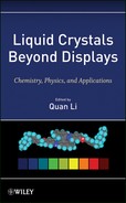
Figure 9.1 shows a schematic representation of the three parts of a semiconducting reactive mesogen. The central aromatic core forms the light-emitting or charge-transporting chromophore. The reactive groups are separated from the aromatic core by flexible aliphatic spacers, which provide solubility and decouple the polymerization sites from the core. The material works as a negative photoresist and Figure 9.2 shows the processing steps leading to the formation of an anisotropic polymer network. Thin films of the monomers are formed by spin-casting, drop-casting, or another solution processing method. The liquid crystalline state may self-assemble spontaneously on the substrate surface as the solvent evaporates, or the sample is heated to attain the mesophase. The liquid crystalline molecules can be macroscopically oriented if there is an appropriate underlying alignment layer. Each monomer has two polymerizable end-groups so that an insoluble crosslinked polymer network is formed by photo- or thermal polymerization in the liquid crystalline phase, the former requiring irradiation with ultraviolet light with the opportunity for photopatterning. The crosslinks ensure that the polymerized network does not show any phase transitions and that it retains its liquid crystalline order through thermal cycling. Figure 9.3 shows a schematic representation of a crosslinked polymer network with nematic order.
Figure 9.1 Schematic of reactive monomer. The ellipse represents the aromatic core of the molecule. The zig–zag lines represent the aliphatic spacers and the squares represent the photo-reactive end-groups.

Figure 9.2 Schematic illustration of the photolithographic process. A thin film of reactive monomers is deposited by solution processing onto a substrate. The sample is irradiated with ultraviolet light through a mask. The irradiated material is photopolymerized and the remaining monomer is rinsed away by washing in the original solvent.
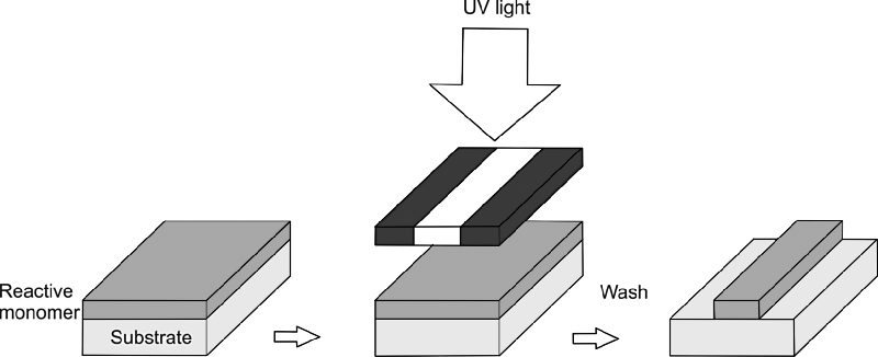
Figure 9.3 Schematic of a crosslinked polymer network with nematic order. The reactive mesogens have photopolymerizable groups attached via aliphatic spacers to each end of an extended aromatic core with semiconducting properties. The mesogens are deposited as a thin film by solution processing. They are polymerized and crosslinked either thermally or by irradiation with ultraviolet light.
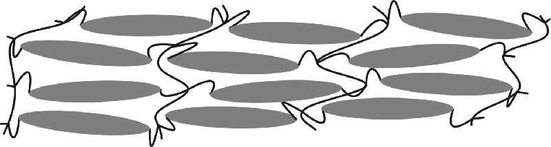
Scheme 9.1 shows the general structures of the polymer backbones formed by polymerization of acrylate, methacrylate, diene, and oxetane reactive groups. The (meth)acrylate monomer polymerizes by a linear radical polymerization reaction to form a relatively flexible poly(meth)acrylate backbone. Cyclopolymerization of the reactive diene group involves a sequential intra- and inter-molecular propagation: the double ring structure is first formed by reaction of the free radical with the second double bond of the diene group [16]. It provides a particularly rigid backbone. This reaction is sterically controlled and is generally slower than the polymerization of the (meth)acrylate compound. Radical photoinitiators, which decompose into free radicals, are necessary to start the polymerization. Usually these are added in very small quantities, normally 1 percent, although quantities as low as 10 ppm have been used [17]. However, the polymerization of some light-emitting reactive mesogens proceeds without a photo-initiator, so avoiding any possible trapping of carriers from the residual photo-initiator [18, 19]. The aromatic core of the reactive mesogen absorbs the light and it is suggested that initiation occurs via thermally assisted energy transfer from the core to methacrylate group; the energy barrier for dissociating the C=C of the reactive group is reduced by 3.1 eV, the absorption energy of the aromatic core. Oxetanes are polymerized by a photocationic, ring-opening mechanism upon irradiation of the monomer doped with a suitable photosensitive catalyst. The protons (H+) released from the catalyst attack the electron-rich oxygen atom in the ring-strained oxetane ring and open it to form a linear poly(oxypropyl) polymer backbone. Free radical polymerization requires the absence of oxygen whereas cationic polymerization has the disadvantage of residual ionic impurities remaining in the crosslinked thin film.
Scheme 9.1 Polymerizable groups and the polymer backbones formed on polymerization.
Photo-differential scanning calorimetry has been used to investigate the extent of crosslinking of the semiconducting reactive mesogen, acrylic acid 6- [20]hexyl estermethyl substituted 1,4-phenylene-bis{4-[6-(acryloyloxy)-hexyloxy]benzoate} 1 (see Table 9.1) [17]. In this experiment the conversion of the photoreactive groups can be calculated from the enthalpy of polymerization. The acrylate end-groups of 1 showed a final conversion of 75 percent on polymerization in the smectic phase at 100 °C. Interestingly polymerization proceeds more slowly and with a lower conversion in the isotropic phase at 120 °C. This is attributed to the favorable alignment of the reactive groups in the smectic phase. Fourier transform infrared (FTIR) spectroscopy has also been used to confirm the crosslinking of reactive groups [18, 19]. However, it is difficult to unambiguously identify the extent of crosslinking because of overlapping FTIR resonances from other transitions in the molecules. As discussed above, one of the main advantages of the crosslinking of semiconducting reactive mesogens is to obtain an insoluble thin film, in order to make multilayer devices. The absorbance spectra of fluorene–thiophene reactive mesogens, for example 2 shown in Table 9.1, were measured before and after rinsing the thin film in the same solvent used for spin-casting the film [18, 19]. The absorbance decreased by 10 percent or less showing the removal of very little uncrosslinked material. There are wide variations in the time taken to crosslink semiconducting reactive mesogens, depending on the photo-initiator concentration, UV source temperature, etc. Thin films of oligofluorenes with variable acrylate content, compound 3 in Table 9.1, were crosslinked in a time of only 30 s [20].
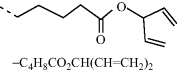
Table 9.1 Reactive mesogens 1 and 2 and polymerizable oligomer 3 used to study the extent or rate of photopolymerization.
| 1 | |
| 2 | 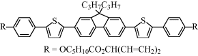 |
| 3 | 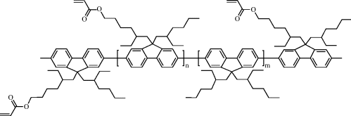 |
| 1: Cr-SmA = 85 oC; SmA-I = 111 oC; SmC- SmA = 66 oC; (acrylate). | |
| 2: Cr-N = 92 oC; N-I = 108 oC; tg = 39 oC; (diene). | |
| 3: n = 0–100 percent; m = 0–100 percent; (acrylate). | |
9.2.2 Optical Properties of Calamitic Reactive Mesogens
Light is absorbed upon transfer of an electron from the highest occupied molecular orbital (HOMO) of a reactive mesogen to its lowest unoccupied molecular orbital (LUMO). These are localized on the aromatic core of the mesogen and have energy EHOMO and ELUMO. Excitons are neutral, bound electron–hole pairs and are formed by the coulombic interaction between the resulting electron and hole. The minimum absorption energy is the exciton energy,
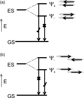
where EBE is the exciton binding energy. Organic materials have large binding energies, ≈0.5 eV, because they are highly localized. The exciton recombines with the emission of a photon of energy ≈Eex. The emission spectrum is broadened and shows multiple peaks because of vibronic coupling. The oscillator strengths of the absorption and emission transitions are affected by intermolecular interactions that depend on the orientational and/or positional order of the mesogens. For example, the molecules of smectic liquid crystals are organized in parallel layers that represent the ideal configuration for the formation of H-aggregates [21–23]. Figure 9.4a shows the splitting of the excited state resulting from intermolecular coupling between a pair of molecules stacked head-to-head. In the lowest energy split state, the transition dipoles of neighboring molecules, indicated by arrows, are oriented in opposite directions so that the net transition dipole is zero and the lowest optical transition is optically forbidden [21]. Hence, H-aggregation gives a blue shift in absorption and can quench luminescence when the excitation relaxes to its lowest state before emission. The magnitude of the splitting varies with the intermolecular spacing that is influenced by the bulkiness of the aliphatic spacers and photoreactive groups. Similarly, as Figure 9.4b shows, the formation of J-aggregates (head-to-tail stacking) can lead to a red shift in absorption and enhanced emission. The formation of H- or J-aggregates depends on the relative displacements of neighboring molecules with nematics forming J aggregates when the longitudinal displacement of neighboring molecules is greater than half the molecular length. The positional order of smectics results in H aggregate formation so that nematics are more suitable light-emitting semiconductors than smectic liquid crystals.
Figure 9.4 Illustration of the splitting of the lowest excited state of an isolated molecule when a (a) H and (b) J aggregates are formed. The combination of the transition dipoles makes the emission symmetry-allowed in the J-aggregate and forbidden in the H-aggregate. Source: Reprinted with permission from O'Neill and Kelly [3]. Copyright © 2010 WILEY-VCH.
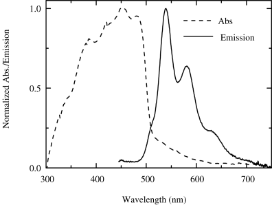
There has been extensive research on nematic reactive mesogens for light emission. For example, the molecule 4, see Table 9.2, has an extended backbone of conjugated fluorene–thipohene units. It absorbs in the near ultraviolet blue region of the spectrum and emits green light as shown in Figure 9.5. It has a photoluminescence quantum efficiency of 39 percent in solution and 35 percent as a thin film [24].
Table 9.2 Extended reactive mesogens 4 and 5 with nematic phases and a non-conjugated 1,4-pentadien-3-yl end-group at the terminus of the aliphatic spacers.
| 4 |  |
| 5 | 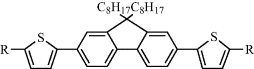 |
| 4: N-I = 188 oC; tg = 26 oC; (diene with no observable melting point). | |
| 5: Cr-N = 52 oC; N-I = 143 oC; tg = 0 oC; (diene). | |
Figure 9.5 Absorption and emission spectra of a thin film of the reactive mesogen 4.
Experiments were carried to investigate whether the photopolymerization of reactive mesogens affects their emission properties [19]. The results depend critically on the conditions that the experiment was done. When the crosslinking was carried out by ultraviolet irradiation at 325 nm in a glove-box with <10 ppm of O2 and water, the photoluminescence quantum efficiency was unchanged within the experimental error of 2 percent. However, photodegradation of the aromatic core was detected by FTIR and photoluminescence when photopolymerization was carried out in an environment containing air and oxygen.
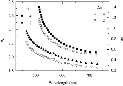
The nematic reactive mesogens 2 and 4 have extended aromatic cores and are very highly birefringent [25, 26]. Figure 9.6 shows the birefringence Δn and refractive index of the extraordinary ray, ne, of 2 and a nonpolymerizable homolog of 4 with six and fourteen aromatic rings, respectively, plotted as a function of wavelength. The highly dispersive nature of ne(λ) results from the π−π* absorption resonances, which peak at 395 nm and 452 nm for compounds 2 and 4, respectively. The dipole moments of the transitions lie along the long axes of the molecules so that ne rather than the ordinary refractive index no is affected by absorption. A maximum Δn value of 0.7 and 1.1 is obtained for the six and fourteen ring compounds, respectively, confirming the expected increase with molecular length. Hence, extremely large anisotropy is also expected in emission making this class of materials useful to obtain polarized electroluminescence, as discussed in Section 3.2.
Figure 9.6 Birefringence, Δn, and refractive index of the extraordinary ray, ne, of 2 and a nonpolymerizable homolog of 4.
The nanoscale patterning of the surfaces of organic semiconductors can significantly alter their emission properties. Current applications include the provision of distributed feedback in organic lasers [27, 28], and enhanced efficiency from OLEDs with corrugated structures [29]. Surface relief gratings were spontaneously formed by the patterned photopolymerization of thin films of reactive mesogen, as illustrated in Figure 9.7 [30]. Light from an ultraviolet HeCd laser was spatially modulated on transmission through a phase mask of period ΛPM and incident to a thin film of the light-emitting, semiconducting reactive mesogen, 5, which has a low melting point. The polymerization-induced change of chemical potential drives mass transfer from regions where there are troughs in irradiance toward the regions containing peaks. A surface grating of period ΛPM or ΛPM/2 is formed spontaneously with no development stage required [31]. Figure 9.8 shows an example of the morphology of a surface grating with period equal to ΛPM. The mass transfer is enhanced by co-operative effects when the incident beam is polarized perpendicular to the grating grooves. Gratings deeper than the original film thickness were also created with a period as small as 265 nm. This period approaches that required, ≈250 nm [26], to make a second order distributed feedback structure for lasing near the emission peak of the material at 510 nm so that the photo-embossing process has major potential for applications in photonics. The mass transfer works well because the material has a nematic phase near room temperature. The compound 4, which has a high clearing point of 188oC and is a nematic glass at room temperature, does not show appreciable mass transfer.
Figure 9.7 A nanostructured surface is spontaneously formed by patterned irradiation of a thin film of a polymerizable liquid crystal. The amplitude of the grating produced is often larger than the original thickness of the film. The material is not washed or etched.
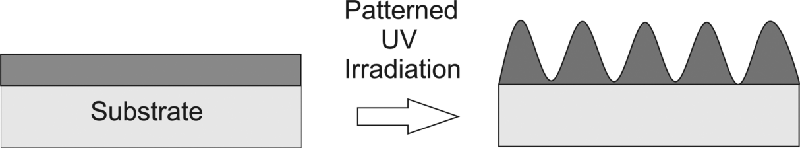
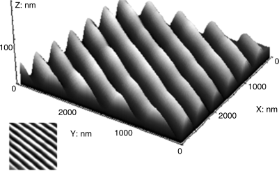
Figure 9.8 Image of surface grating formed by irradiation of a thin film through a phase mask of period 530 nm. The surface grating has the same period and average depth of ≈60 nm. The image was obtained using atomic force microscopy. Source: Reprinted with permission from Liedtke et al. [29]. Copyright © 2010 American Chemical Society.
9.2.3 Electrical Properties of Calamitic Reactive Mesogens
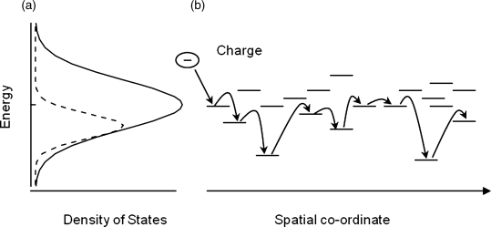
Liquid crystals are relatively disordered compared to molecular crystals, so a coherent band-like description of charge-carrier transport in liquid crystals is inappropriate. Instead a thermally activated hopping model is used. The intersite hopping of electrons or holes occurs via π–π interactions between the sites, which usually are single molecules but may be traps [32]. The hopping rate depends on the strength of the electronic coupling between the HOMOs (LUMOs) of adjacent molecules, and exponentially decreases with intermolecular separation. Charge transport is characterized by the carrier mobility (μ), defined as the electron or hole velocity per unit electric field. Smectic reactive mesogens are expected to show high mobility in two dimensions because of their positional order and small intermolecular separation. Charge transport between the layers would be significantly slower. Disorder-based empirical models, for example that derived from the Monte-Carlo simulations of charge transport by Bässler et al. [33], have been used to discuss the temperature and electric field dependence of mobility for both smectic and nematic reactive mesogens [34–37]. The electronic density of states is broadened by disorder (see Figure 9.9) and may be represented by a Gaussian distribution, whose width depends on variations in the local conformation of the molecule, structural defects, dipolar disorder due to random orientation of polar groups, etc. The mobility increases with temperature as more energy is available to overcome the barriers for hopping between neighboring states created by energetic disorder. Positional disorder is caused by variations in the relative positions and orientations of molecules and results in a distribution of electronic couplings within the material. The mobility of smectic reactive mesogens is weakly temperature dependent, implying a small energetic disorder according to the Bässler model [34].
Figure 9.9 (a) The density of LUMO states (solid line) and occupied LUMO states (dashed line) for a disordered, liquid crystalline semiconductor. (b) The horizontal lines indicate energy levels of individual molecules in a disordered ensemble of molecules. The sequence of arrows shows an arbitrary pathway for an electron through the molecular ensemble. Hopping to a higher energy state requires activation energy and so is less likely than hopping to a lower energy state.
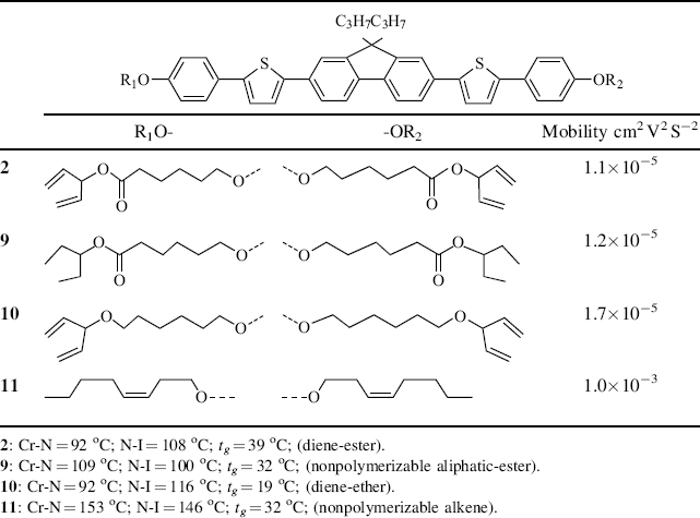
The charge carrier mobility in the plane of the device can be obtained from a field-effect transistor as explained in more detail in Section 4. Time-of-flight experiments are used to probe charge transport from top-to-bottom of a thin layer [36]. The molecules must be homogeneously aligned (in the plane of the film) so that intermolecular hopping can proceed in the right direction. The mobility of reactive mesogens (6 and 7, see Table 9.3) was studied at elevated temperatures in the smectic G phase and compared to a non-reactive analog, 8. Ambipolar charge transport was observed. The diene and oxetane reactive mesogens have lower mobility and are less ordered than the non-reactive species, whose hole mobility is 0.044 cm2 V−1 s−1. On polymerization the mobility of the oxetane reactive mesogen 6, increases, from 0.01 cm2 V−1 s−1 to 0.033 cm2 V−1 s−1 for holes, while that of the diene mesogen decreases. An experiment was carried out to check whether the polarizable nature of the ester or diene end-group significantly reduces the hole mobility of nematic mesogens. As shown in Table 9.4, compounds 2, 9, and 10 have the same aromatic core and branched end-group of similar length and shape, but have large differences in the polarizability of the end-group. All three compounds have very similar hole mobility values at room temperature. These values are almost 2 orders of magnitude smaller than that of compound 11, which has unbranched end chains. This suggests that it is the shape of the end-group rather than its polarizable nature that limits the transport of holes.
Table 9.3 Semiconducting reactive mesogens 6 and 7 with smectic phase and either a photopolymerizable oxetane or a non-conjugated 1,4-pentadien-3-yl end-group, respectively, at the terminus of the aliphatic spacers and their nonpolymerizable diheptyl-substituted homologue 8
| R1 | R2 | |
| 6 |  |
 |
| 7 | 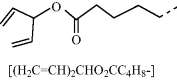 |
 |
| 8 | ||
| 6: Cr-SmG = 83 °C; SmG-SmB = 93 °C; SmB-I = 144 °C; (oxetane) | ||
| 7: Cr-SmG = 75 °C; SmG-I = 174 °C; (diene) | ||
| 8: Cr-SmG = 140 °C; SmG-SmC = 225 °C; SmC-SmA = 229 °C; SmA-I = 234 °C; (nonpolymerizable aliphatic chains). | ||
Table 9.4 Room temperature mobility of nematic compounds 2 and 9–11. Compounds 9–11 have the same aromatic core as 2 but different terminal groups as shown in the table. Compound 2 is a reactive mesogen and 9–11 have nonpolymerizable end-groups.
9.3 OLEDs
9.3.1 Principle and Applications
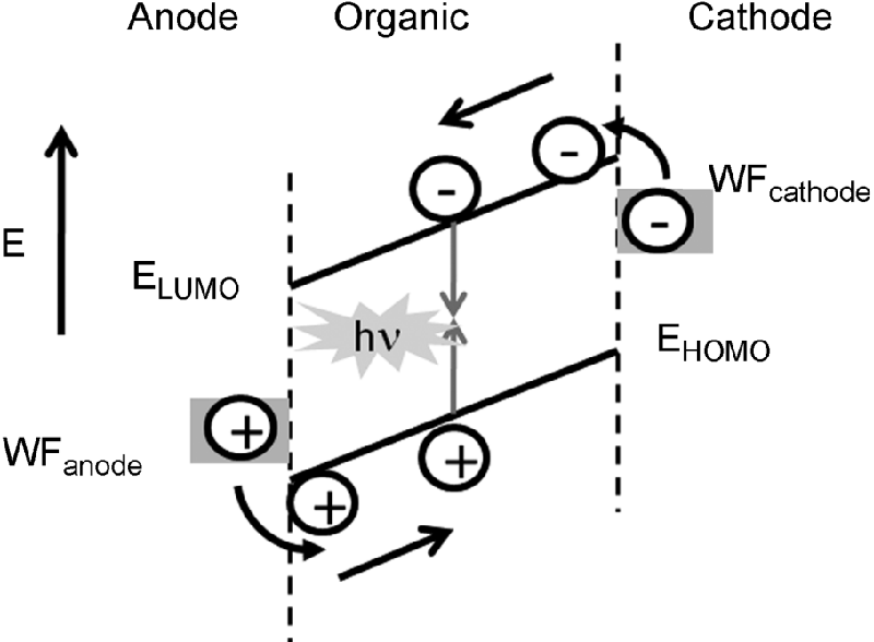
Electroluminescence is the generation of light other than the black-body radiation by electrical excitation and was pioneered in molecular and polymeric thin film devices by groups in Kodak, and Cambridge [1, 2]. Figure 9.10 shows a schematic representation of an OLED containing a light-emitting semiconducting organic layer sandwiched between two dissimilar electrodes. An energy level diagram of the device is given in Figure 9.11, showing the built-in field originating from the difference in the work-functions of the two electrodes [38]. Electrons are injected from the cathode into LUMOs of the molecules at the interface. Similarly holes are injected from the anode into the HOMOs (electrons are removed from the HOMOs). The charged carriers drift in the applied field by thermally activated hopping from molecule-to-molecule, at a rate depending on the strength of the electronic coupling between the HOMOs (LUMOs) of adjacent molecules. The color of the emitted light can be tuned from blue to red by modification of EHOMO and ELUMO (see Eq. (9.1)) using chemical design [39]: an electron donating group can be added to increase EHOMO whereas electron-withdrawing groups decrease ELUMO. The luminescence exits the device through one of the electrodes. Often the anode is made from indium tin oxide (ITO), which is transparent. The work-function of ITO is about 4.7 eV, which presents a large barrier for hole injection for most organic materials, when EHOMO typically varies between 5.1 eV and 5.8 eV. Hence the conductive polymer poly-(3-4-ethylenedioxythiophene)/poly-(styrene sulfonate) (PEDOT:PSS), which has a work-function tunable over a limited range, is often inserted between the anode and the organic light-emitting film to improve the injection of holes [40]. Low work-function metals, for example Ca or Mg, are often used as cathodes to minimize the barrier for electron injection. However, these are unstable and must be capped with an inert metal, Al or Ag. Alternatively high work-function metals such as Al are used in conjunction with a thin insulating buffer layer, for example LiF or CsF, which improve electron injection by band bending [41]. Multiple organic layers are often used to stagger the injection barriers that are particularly large for blue emission. Hole/electron blocking layers at the cathode/anode may be introduced to confine carriers in the emission layer. Exciton blocking layers are used to prvent excitons from reaching the electrodes where they can be quenched. Multi-layer devices are easy to implement for small molecule OLEDs where the organic films are deposited by thermal evaporation in vacuo. Polymeric films are normally deposited by solution processing so that orthogonal solvents are needed to avoid layer mixing.
Figure 9.10 Schematic of an OLED consist a thin film of a light-emitting organic semiconductor sandwiched between cathode and anode. Light is emitted on application of a forward bias.
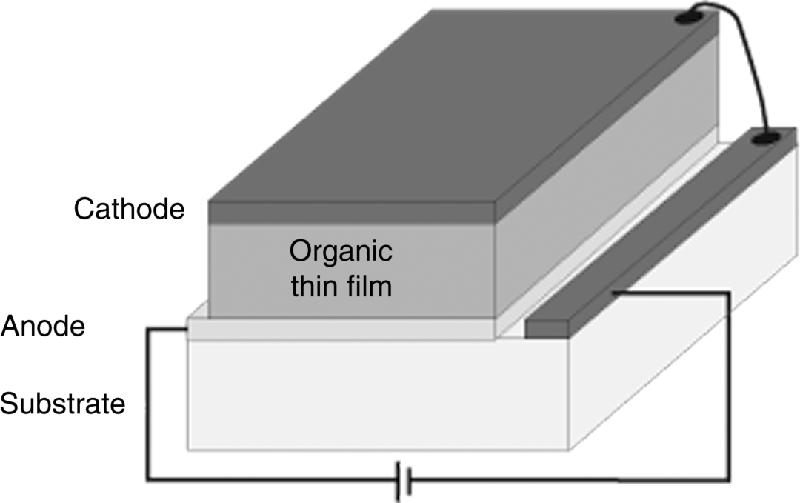
Figure 9.11 Energy level diagram of OLED showing the HOMO and LUMO energy levels, EHOMO and ELUMO, of an organic thin film sandwiched between anode and cathode of work-functions WFanode and WFcathode, respectively. The levels are tilted because of the built-in field. A photon of energy hν is emitted as defined in Eq. (9.1).
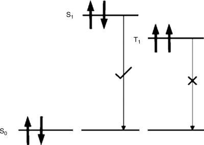
The exciton is formed from two independent charges of spin ±1/2 giving either an excited singlet (S = 0) or triplet (S = 1) state, as illustrated in Figure 9.12. The formation of exciton triplet states by electron–hole capture is three times more likely than singlet formation, if the process can be assumed to be spin independent. As discussed above, spin-allowed radiative emission (fluorescence) is from the singlet only, so that the formation of triplets represents a significant energy loss, especially, when the exchange energy is large, inhibiting cross-over from the red-shifted triplet to the singlet. Triplet excitons can produce light by phosphorescence but this process is inefficient for organic materials. Metallo-organic complexes are often used as phosphorescent dopants in OLEDs [42]. The spin–orbit coupling produced by the heavy atom increases the rate of the forbidden transition from the triplet to the singlet ground state.
Figure 9.12 Schematic of ground singlet state (S0), first excited singlet (S1) and triplet (T1), states. The S1 →S0 transition is allowed and the T1 →S0 transition is forbidden.
The external efficiency of the OLED is given by
(9.2) ![]()
where γ is the ratio of the number of excitons within the device to the number of electrons in the external circuit; χS is the fraction of singlet excitons. ηPL is the photoluminescence quantum efficiency of the emitter; ηC is the fraction of photons coupled out of the device. There are many issues that affect the efficiency of an OLED. It is important to balance the injection of electron and holes and mobility should be high for both, so that space charge effects do not significantly impede charge injection. The luminescent material must have high quantum efficiency. Indeed the requirements for high mobility and high luminescent efficiency can be contradictory. Good charge transport require strong intermolecular coupling but the related aggregate may quench luminescence, as discussed in more detail in Section 9.2.2 [43]. The outcoupling efficiency of the OLED depends critically on the device configuration. The rear electrode acts as a mirror setting up standing waves so that optical mode pattern and recombination zone must be matched for efficient outcoupling of the light. ηC is also limited by total internal reflection that traps photons, emitted at large angles to the normal of the device, within the organic thin films and substrate. Finally, the materials must be photochemically, thermally, and electrochemically stable to maintain long-term operation.
The two main classes of OLEDs are based on conjugated small molecules and polymers, respectively. The more advanced technology, which is commercially widely available, involves small molecules that are deposited by thermal evaporation in vacuo. Shadow masks are used to define pixels. Polymer electroluminescence is less well-developed commercially but has potentially much lower fabrication costs because it uses solution processing. Ink jet printing can provide multi-colored displays. OLEDs are considered future competitors of LCD TVs particularly for high-end markets, because of their wider viewing angles, higher efficiency, very high contrast, and darker gray levels as well as their faster response times. OLEDs are gaining an increasing share in the market of small area displays for mobile phones, organizers, etc. The processing of large area displays has yet to be optimized and differential aging of the different color pixels remains a problem. Efficacies up to 70 cd A−1, 28 cd A−1 and 8 cd A−1 have been achieved for green, red, and blue materials, respectively. White-light electrophosphorescence is now considered as a practical and efficient method for solid-state lighting [44]. Large area, color tunable, panels are anticipated and the first products are already available for specialized applications.
The initial interest in polarized EL was to provide a polarized OLED backlight for LCDs, eliminating the need for expensive polarizers, fluorescent tubes and diffusers/lightpipes. The polarization ratio R gives the ratio of the measured intensity of polarized light parallel and perpendicular to the alignment direction, as measured using an analyzer. It is used as a practical figure of merit. R values between 12 and 200 are required depending on the application, to avoid the use of a “clean-up” polarizer. This approach is considered as a useful market-entry product for OLEDs; a relatively unsophisticated unpixellated white-light or monochrome display is required when the image processing is carried out using the well-established addressing schemes of the liquid crystal display. High luminance levels are required from the OLED to compensate for losses through the display and filters. The compact nature of the OLEDs would give a slimmer display. A major potential market for OLEDs is in emissive displays for mobile phones, camcorders, and personal digital assistants. Many of these are viewed in bright sunshine and the image can be washed-out by reflection of sunlight transmitted into the display by the metal cathode. Linear polarizers at the output to the display are sometimes used to improve viewing in daylight since at least half of the incident sunlight is absorbed by the polarizer. The benefits of polarized OLEDs are obvious; the electroluminescent image has minimal loss on passage through the output polarizer.
9.3.2 Polarized Electroluminescence Using Reactive Mesogens
9.3.2.1 Introduction
Polarized electroluminescence requires the uniform planar alignment of the light-emitting LC. This is normally obtained using an alignment layer located between the anode and the light-emitting film. Hence, the alignment layer must also be able to transport holes injected from the anode. Hole transport in disordered organic materials occurs by hopping between molecules with high values of EHOMO. Intra- and inter-chain hopping occurs in conjugated polymers. The probability of hole transfer has an inverse exponential dependence on the intermolecular separation so that a reasonably high concentration of the hole transporting component is required. The alignment/charge transporting layer is normally deposited by spin-coating and uniaxial in-plane anisotropy is developed, either by mechanical rubbing in one direction or by photoalignment, as discussed below. It is thought that the rubbing of a polymer thin film results in the uniaxial orientation of the polymer chains near the surface of the film. The emission layer is then deposited on top and uniformly oriented in the direction imposed by the alignment layer by annealing in the liquid crystalline phase. The alignment is frozen-in by polymerization of the reactive mesogens either by annealing or by irradiation with UV light on cooling. Finally, a metallic cathode is deposited by thermal evaporation. The transition dipole moment of a calamitic liquid crystalline emitter is normally oriented along the long molecular axis. This determines the electric field direction of the emitted light so that the resulting polarization of the emission depends on the order parameter of the nematic [45]. The relationship is more complex than for absorption when the fluorescence tensor is of fourth order, because it results from the product of two second rank tensors, namely the absorption and emission.
9.3.2.2 Photoalignment
The process of mechanical rubbing produces dust and scratching, which can be expected to severely affect the yield and performance of thin layer OLEDs. These problems are expected to be more severe than in liquid crystal displays, because the electroluminescent film is typically about 50 nm thick. Mechanical damage may also result in short circuits and so-called “black-spots”. These problems are avoided completely using non-contact photoalignment techniques first developed for LCDs [46, 47]. Illumination of the photoalignment film with polarized light generates a surface anisotropy in the alignment layer. When the LC film is deposited on top, the directors orient along with easy axis of the alignment layer, on annealing in the nematic phase. An added advantage is that the polarization direction of EL can be patterned photolithographically by patterning the polarization direction of the incident beam.
Coumarin side-chain polymers have been extensively used as photoalignment materials for nematic LCs for liquid crystal displays. On irradiation with linearly polarized light, the probability of a photochemical reaction is proportional to cos2ϕ where ϕ is the azimuthal angle between the polarization direction P of the incident beam and the transition dipole moment of the coumarin side-chain. According to Schadt et al. [48], the coumarin side-chains are depleted anisotropically by a 2 + 2 cycloaddition, as illustrated in Scheme 9.2. The nematic liquid crystal is subsequently deposited and aligns homogeneously with its director-oriented parallel and perpendicular to P for weak and strong polarized UV illumination, respectively [49]. Spectroscopic analysis shows that the competition between two independent LC–surface interactions determines the resultant director orientation. Parallel LC alignment is determined by a short-range steric interaction with the dimerised cyclobutane side-chains. The LC alignment direction switches from parallel to perpendicular above a critical influence and subsequently the LC alignment is determined by a dispersive LC interaction with the intact side-chains in the bulk of the photoalignment layer. A key advantage of the use of side-chain coumarins as photoalignment polymers is their thermal stability resulting from crosslinking, especially in the parallel alignment regime.
Scheme 9.2 Chemical structures of coumarin group used for liquid crystal photoalignment before and after irradiation with polarized light. P indicates the polarization direction of the incident ultraviolet light.
9.3.2.3 Progress in RMs for Polarized OLEDs
Polarized photoluminescence from an LC network was first demonstrated using a polymerizable mixture (Cr 116°C, N 150°C, I) of a photoinitiator, a thermal inhibitor dissolved in the non-luminescent reactive mesogen 12 and a guest luminescent diacrylate 13 shown in Table 9.5 [50]. The photoluminescence polarization ratio was 13:1. The acrylate 14 was synthesized by adding polymerizable acrylate end-groups to a light-emitting phenylenevinylene molecular fragment to form a similar reactive mesogen to the diacrylate 12 [51]. However, the acrylate 14 is luminescent due to the presence of the carbon–carbon double bonds [vinylene groups, –CH=CH–] in place of the carboxy groups [COO] in 12. The former was aligned in the liquid crystalline state on a rubbed polyimide layer and then polymerized by heating up to a temperature of 180°C to form an anisotropic polymer network. The R value was only 3.5 using photoluminescence. This low polarization ratio could partly be attributed to a low order parameter related to high temperature annealing, which was necessary because the acrylate 14 is crystalline at room temperature. Suitable molecular engineering allows the synthesis of reactive mesogens with much lower melting points and a nematic phase at room temperature. For example, the reactive mesogen 2 forms a nematic phase between 92°C and 108°C and maintains nematic order in a glassy state on cooling to room temperature. The compound has a glass transition temperature of 39°C. An efficient method was devised to prepare well-defined fluorene oligomeric blends with two acrylate end groups by end-capping [52]. For example, a blend 15 containing a mixture of fluorene trimers (n = 1), pentamers (n = 3), heptamers (n = 5), and nonamers (n = 7) forms supercooled nematic phases with no sign of crystallization upon cooling. The clearing point varies with molecular weight and was as low as 100°C.
Table 9.5 Reactive mesogen 12, guest luminescent diacrylate 13, host reactive mesogen 14 and the polymerizable nematic oligomer 15 used for polarized luminescence.
| 12 |  |
| 13 | 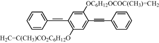 |
| 14 | 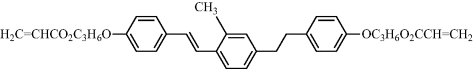 |
| 15 | 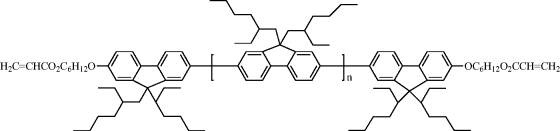 |
| 12: Cr-N = 86°C; N-I = 116 °C; tg = 39°C; (host). | |
| 13: Cr-I = 80°C; (luminescent dopant). | |
| 14: Cr-SmA = 90°C, SmA-N = 144°C, N-I = 210°C. | |
| 15 N-I = 170°C; tg = 80°C; (Mw = 600 g mol−1 by GPC; no melting point). | |
Table 9.6 shows the coumarin phototalignment polymers (16 and 17) used to align reactive mesogens for polarized electroluminescence. The first polarized electroluminescent device using reactive mesogens was obtained by depositing 2 from solution by spin casting on a coumarin photoalignment polymer 16 that was previously irradiated with polarized UV light [53]. The photoalignment layer was doped with 4,4′,4″-tris(1-naphthyl)-N-phenyl-amino)-triphenylamine, 18 (see Table 9.7), to aid hole injection from the ITO electrode to the light-emitting film. The LC 2 was deposited, heated to 100oC and it was aligned spontaneously while slowly cooling to 20oC to form a nematic glass. The alignment was locked in by the formation of an anisotropic polymer network through photopolymerization at room temperature. Figure 9.13 shows the electroluminescent spectra for the orthogonal polarization directions. A maximum R value of 10:1 was obtained, limited by the order parameter of small molecules. The alignment direction was parallel to the polarization direction of the UV beam, independent of the irradiation conditions of the photoalignment layer. This implies that alignment is governed by the interaction of the LC with the coumarin photoproduct rather than the unreacted coumarin. However, REL depended on the fluence used to align the photopolymer as well as on the concentration of the hole transporting dopant, 18. The latter has a tetrahedral pyramidal shape and so inhibits the photogeneration of anisotropy in the photoalignment layer, so that high polarization ratios were only obtained when the 18:16 ratio was less than 30 percent. However, the maximum irradiance of 90 cd m−2 required an equal fraction of 18 and 16 in the alignment/hole transporting film.
Table 9.6 Coumarin polymers used to align reactive mesogens for polarized electroluminescence.
| 16 |  |
| 17 | 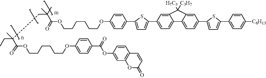 |
| 16: homopolymer tg = 60oC. | |
| 17: copolymer n:m = 4:1; tg = 69oC. | |
Figure 9.13 Polarized electroluminescence spectrum from a thin film of 2 taken (i) parallel and (ii) perpendicular to the alignment direction of a doped photoalignment layer. Source: Reprinted with permission from Contoret et al. [53]. Copyright © 2000 WILEY-VCH.
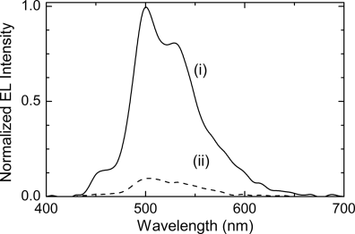
Table 9.7 4,4′,4″-tris[N-(1-naphthyl)-N-phenyl-amino]-triphenylamine used as a hole transporting dopant in the photoalignment layer 16
| 18 | 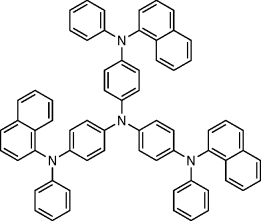 |
| 18: tg = 106oC; (triaryl amine dopant). | |
Various strategies were investigated to optimize the alignment and hole injection properties of the alignment layers. A fluorene pentamer with polymerizable groups at the end of two aliphatic spacers is liquid crystalline at room temperature. It was aligned on a thin-rubbed polyphenylene vinylene (PPV) alignment layer and subsequently crosslinked to form a light-emitting polymer network with polarized emission [54]. PPV has a relatively low EHOMO of 5.2 eV, facilitating hole injection. A REL value of 25 was obtained from a similar oligomer but the EL spectrum was broadened either by excimer emission or luminescence from the rubbed PPV alignment layer. Alternatively a copolymer with both coumarin and linear hole-transporting side-chains, polymer 17, was developed as a photoaligning and hole injection film. The hole-injection unit has the same fluorene–thiophene aromatic core as the light-emitting mesogen, 2 [55, 56]. Both 2 and 17 have the same value of EHOMO, equal to 5.6 eV, so that their hole injection properties are similar. However, the mobility of 17, which could not be measured by time-of-flight, is expected to be much lower than that of 2, equal to 1.1 × 10⁻⁵ cm2 V−1 s−1, because of the low density of fluorene–thiophene side-chains (=20 percent) in the copolymer [36]. Polymer 17 was incorporated between the anode and the light-emitting film in a linearly polarized OLED. The light-emitter 5 had a longer thiophene–fluorene mesogen than 2, to give a higher order parameter. The device had a luminance of 300 cd m−2 at 10 V and a maximum efficacy of 1.6 cd A-1. REL had a maximum value of 13. Polarized electroluminescence with REL = 31 was obtained from extended liquid crystalline oligomers (non-polymerizable), which were aligned using a rubbed PEDOT/PSS layer [57].
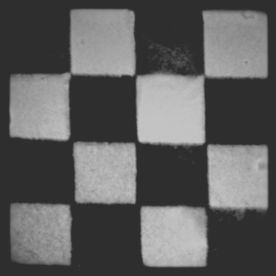
As mentioned above, the alignment direction of the liquid crystalline emitter, and consequently the polarization direction of the emitted light, can be spatially patterned when photoalignment techniques are employed. This forms the basis of a three-dimensional display. The principle is illustrated in Figure 9.14. Each pixel can be subdivided into two subpixels having orthogonal polarization directions of emission simply by irradiating the adjacent subpixels of the photoalignment film with orthogonally polarized light. The two sets of subpixels create two separate images with orthogonal polarization. A three-dimensional effect is created when viewed through glasses having orthogonally polarized lenses; each eye sees a different image. This presents a low-cost solution for a three-dimensional display with applications in entertainment and medicine. The ability to pattern the polarization of electroluminescence may also have security applications as images can be generated that are only viewable through a polarizer. Figure 9.15 shows PL from a uniform layer of compound 5 deposited onto a photoalignment film of compound 17, patterned by exposing adjacent squares with orthogonally polarized light. The photoluminescence image is viewed through a polarizer, and the green and dark regions are orthogonally aligned. Rotation of the polarizer by 90° changes the black pixels to green and vice versa. This demonstrates the potential of the technology to make a three-dimensional display.
Figure 9.14 Illustration of principle of three-dimensional display using subpixels with orthogonally polarized emission. The symbols ![]() and ↔ represent vertically and horizontally polarized light, respectively.
and ↔ represent vertically and horizontally polarized light, respectively.
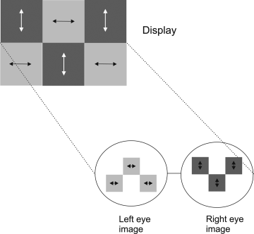
Figure 9.15 PL from compound 5 deposited onto a photoalignment film of compound 17, patterned by exposing adjacent squares with orthogonally polarized light, viewed through a polarizer. The green and dark regions are aligned orthogonally. Source: Reprinted with permission from Aldred et al. [55]. Copyright © 2005 WILEY-VCH.
9.3.3 Pixellated Devices
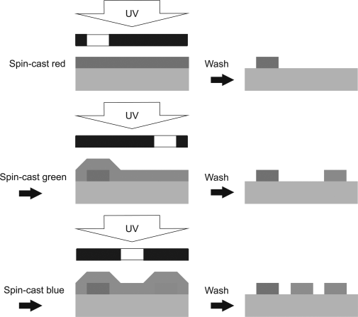
Photolithography is the dominant patterning technique in the semiconductor industry, because of its high resolution, precise registration, fast throughput, and the ability to cover large areas. The photolithographic polymerization of light-emitting reactive mesogens is therefore a promising alternative route to ink-jet printing for a full-color display, with the added advantage of multi-layer capability; irradiation fixes the lower layer of a pixel before deposition of a second, this process is shown in Figure 9.16. A thin red-emitting film is deposited by solution processing, irradiated by UV light through a mask to define an insoluble pixel and the remaining materials removed by washing in chloroform. Pixels of the green and blue light-emitting materials are then sequentially formed in different regions by a similar process. It is important to deposit the red material first. Otherwise small quantities of the red-emitting material could remain as a dopant in the green or blue pixel after washing. Energy transfer from the host to the dopant would result in some unwanted red emission from these pixels.
Figure 9.16 Photolithographic process to produce a red, green, and blue pixellated OLED. After patterned irradiation with ultraviolet light, the sample is washed with the solvent used for deposition, so that the unexposed regions are removed. (See the color version of this figure in Color Plates section.)
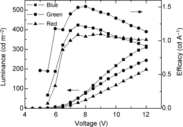
A pixellated red, green, and blue liquid crystal OLED was prepared by photolithography as described above [55]. Tables 9.2 and 9.8 show the chemical structures and transition temperatures of the blue, green, and red-emitting materials numbered 19, 5, and 20, respectively. Their emission spectra are shown in Figure 9.17. Both compounds 19 and 5 are nematic reactive mesogens, which exhibit a metastable supercooled nematic phase for room temperature processing over long periods. Compound 20 is a nematic liquid crystal, which is a crystalline solid at room temperature and therefore it was used in a guest–host configuration to obtain a room temperature nematic phase. The red-emitter contained a blend of 20 in 5, mixed in a ratio of 1:3. Red electroluminescence was observed because of efficient energy transfer from the host to the guest. The full color OLED with RGB pixels on the same substrate was fabricated as described above and is shown in Figure 9.18. UV light from a HeCd laser at 325 nm was used to photopolymerize the reactive mesogens. Figure 9.19 shows the irradiance and the efficacy of the three pixels as a function of voltage. Each pixel switched on at about 6 V. Electroluminescence was most efficient (1.5 cd A−1) from the green pixel.
Table 9.8 Chemical structure of the blue and red-emitting reactive mesogens 19 and 20
| 19 |  |
| 20 |  |
| 19: Cr-I = 80oC; N-I = 39oC; tg = –2oC; (diene). | |
| 20: Cr-N = 142oC; N-I = 123oC; tg < 15oC; (diene). | |
Figure 9.17 Electroluminescence spectrum of 19, 5, and 20, respectively. Source: Reprinted with permission from Aldred et al. [55]. Copyright © 2005 WILEY-VCH.
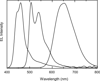
Figure 9.18 A prototype OLED with a red, green, and blue pixel on the same substrate fabricated by sequential spin-coating and polymerization of the materials 20, 5 blend, 5 and 19 onto a PEDOT:PSS film covering a patterned indium tin oxide (ITO) substrate. The pixels were defined by irradiation at 325 nm through a mask. Non-irradiated material was removed by washing with chloroform. The pixels were coated with a hole-blocking film of 3-(4-biphenylyl)-4-phenyl-5-tert-butylphenyl-1,2,4-triazole and capped with a LiF/Al electrode. Source: Reprinted with permission from Aldred et al. [55]. Copyright © 2005 WILEY-VCH. (See the color version of this figure in Color Plates section.)
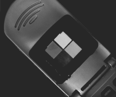
Figure 9.19 Luminance and efficacy from the blue, green and red pixels of the device shown in Figure 3.18.
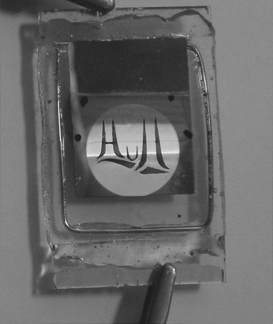
The photolithographic process can also give a new type of color-graded image using partial photopolymerization [25]. Figure 9.20 shows a photograph of an operating, single pixel, multicolor OLED, prepared by the sequential deposition of the red, green, and blue materials 20, 5, and 19. The red material was deposited first, irradiated through a mask and washed to remove the unirradiated material. The green and blue materials were then processed similarly with the crosslinked green region partially overlapping the insoluble red film and the crosslinked blue partially overlapping the green. This results in blue–green and green–red emission, because there is some electroluminescence from both layers in the overlapping regions. A closer look at Figure 9.20 shows that the overlapping green–red region has two distinct zones giving yellow and orange EL. This arises because the red material in the overlapping region is not uniformly thick because the irradiation conditions were spatially varied to give nonuniform and incomplete polymerization resulting in partial removal of the film on washing. The photograph was taken at an operating voltage of 5 V. The threshold voltage for electroluminescence varied between 3.5 V and 4 V across the device.
Figure 9.20 Photograph of graded-color single pixel OLED operating at 5 V. The logo represents the Humber Bridge located near Hull, England. This is one of the longest single span bridges in the world.
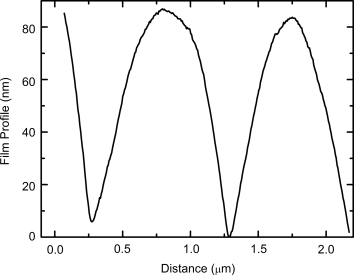
Micron scale resolution is possible with the photolithographic process [20, 25], as shown by exposing a thin film of 5 through a phase mask of period 1 µm in soft-contact with the film. The phase mask produces a spatially modulated irradiance pattern with the same period as the phase mask; the exact spatial distribution of the irradiance depends on the relative intensity of the different diffraction orders of the grating [58]. The sample was then washed with chloroform to remove the soluble material. Figure 9.21 shows the surface profile of the washed film measured by atomic force microscopy. A surface relief grating is formed with a period equal to that of the phase mask. The non-crosslinked material in the minimally exposed regions is completely removed while the fully crosslinked material in the maximally exposed regions is retained. A grating thickness of ≈85 nm is obtained.
Figure 9.21 The surface profile, obtained using atomic force microscopy, of the washed polymer network film produced by irradiation of monomer 5 through a phase mask of period 1 µm. The period of the surface profile is equal to that of the phase mask.
9.4 Organic Field-Effect Transistors
9.4.1 Principle
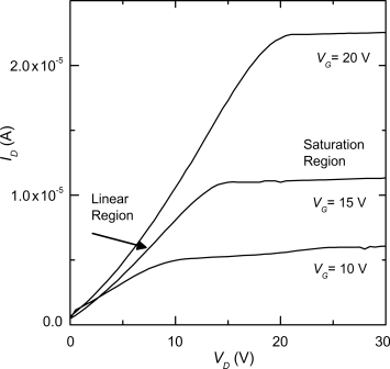
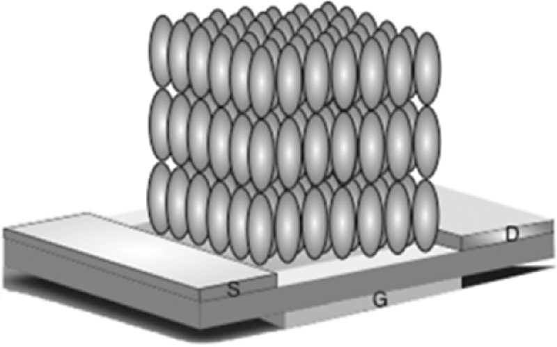
Transistors are organic semiconductor devices use to amplify and switch electronic signals. In an OFET a voltage applied to the gate electrode controls the current between the source and drain electrodes [59, 60]. The construction of a typical OFET is shown in Figure 9.22. An insulator is placed between the gate and the organic semiconducting thin film. The source and drain electrode are separated using semiconducting channel of length L and width W. Ideally, when no gate voltage, VG, is applied, the conductance of the semiconductor film is extremely low because there are no mobile charge carriers, that is, the transistor is “off”. The application of VG gives an electric field across the dielectric, which induces mobile charges in the semiconductor film. These move in response to the voltage, VD, applied between the source and drain, that is, the transistor is “on”. Figure 9.22 is an example of a bottom-gate, top-contact device configuration. The source and drain electrodes may be deposited between the dielectric and semiconducting thin film giving a bottom-gate, bottom-contact device. Alternatively the layers can be applied sequentially in the order: source and drain electrodes, semiconducting thin film, insulator, and gate electrode giving a top-gate configuration. Figure 9.22 also shows the circuit used to test the OFET. The source electrode is placed at ground. A hole (electron) drain current, ID, is measured when a negative (positive) VG is applied. VG must be greater than a threshold value VT, before current flows because the contacts may not be ohmic and charge-carrier traps must first be filled. Figure 9.23 shows the output characteristic curve of the transistor, that is, a plot of ID versus VD for different values of VG. Two regions of the characteristic curve can be differentiated: ID increases approximately linearly for low values of VD, is when VD ![]() (VG − VT). When (VG − VT) > VD, ID saturates. The physics underlying these characteristics is beyond the scope of this volume and is well explained elsewhere [60].
(VG − VT). When (VG − VT) > VD, ID saturates. The physics underlying these characteristics is beyond the scope of this volume and is well explained elsewhere [60].
Figure 9.22 Schematic of an OFET. The gate electrode G is deposited on a substrate. The dielectric layer and p-type organic semiconducting film are deposited sequentially on top. The source S and drain D electrodes are photolithographically patterned to define a channel of width W and length L. The gate and drain voltages are VG and VD, respectively, with corresponding notation for current I.
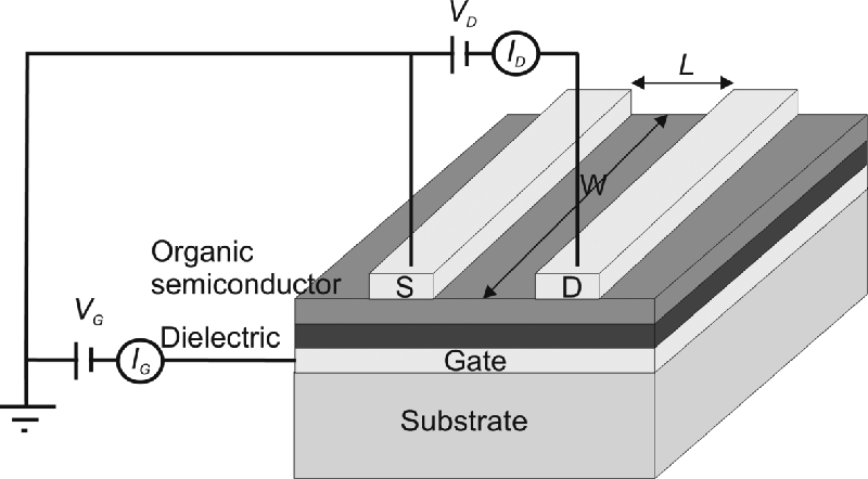
Figure 9.23 Output characteristics showing ID versus VD of a typical OFET.
The charge-carrier mobility μFET is a key parameter obtained from the characteristics. It can be determined from the linear region using the equation
(9.3) ![]()
where C is the capacitance per unit area of the insulator. Alternatively, keeping VD constant in the saturation region, μFET can be calculated from a plot of ID versus (VG − VT)2 using the equation
(9.4) ![]()
It is desired to maximize the magnitude of μFET so that the operating voltage and power consumption of the transistor can be minimized. Another important parameter is the on/off ratio, equal to ID (on)/ID (off), which should be sufficiently large to define the states “0” and “1” in an electronic circuit.
Both the conjugated polymers, small molecules and blends of both material types are investigated as organic semiconductors and some materials show mobilities >1 cm2 V−1 s−1 [61, 62]. The market for organic electronics is at a very early stage with first products such as printed batteries and sensor on stream. Radio frequency identification (RFID) is a technology that allows all products to have a unique identifier, which is machine readable without line of sight. This gives a major impetus for the development of organic electronics because it requires very low-cost electronics. Electronic security provides another incentive for devices and systems that are easy to integrate, hard to simulate and simple to check. Smart packaging is expected to be another major application area with the potential to enhance the attractiveness of products.
9.4.2 Progress in Reactive Mesogens for OFETs
As discussed in Section 2.3, low-molar-mass smectics self-organize in layers with order in two dimensions. In the smectic A and C phases, the packing in the layers is fluid-like, while the more ordered, crystalline smectics, with hexatic, hexagonal, or herring-bone packing, facilitate greater π–π overlap. The resulting short intermolecular separations give large π–π coupling and the potential for fast intermolecular hopping. Silane-based surfactants are generally used to give the required homeotropic alignment to provide in-plane transport between the electrodes of OFETs (see Figure 9.24). OFETs operate at room temperature so that materials are required with a smectic phase at room temperature and with an extended temperature range to ensure thermal stability. This is a considerable constraint on the design of suitable materials. An alternative way to ensure operating stability is to lock-in the smectic phase of a thin film of a reactive mesogen by polymerization. OFETs fabricated from both crosslinked and uncrosslinked thin films of the smectic reactive mesogens, compounds 6 and 7, were studied [63–65]. The mobility of 7, which has a diene reactive group, was 0.01 cm2 V−1 s−1 before crosslinking but decreased by a factor of 10 after photopolymerization in the high temperature crystalline smectic G phase. A similar trend was obtained elsewhere for an OFET constructed with the quaterthiophene acrylate 21, whose structure is shown in Table 9.9 [65]. However, this result may not be general. The field-effect mobility of 6 increased after crosslinking, albeit from a very low value of 8 × 10⁻⁵ cm2 V−1 s−1. The same material showed time-of-flight mobility values, recorded at 140°C, of 1 × 10⁻² cm2 V−1 s−1 before polymerization and 3 × 10⁻² cm2 V−1 s−1 afterwards [66]. Crosslinking was also shown not to degrade charge transport in an OFET based on star-shaped molecules and in a nematic reactive mesogen with a diene photoreactive end-group studied with time-of-flight measurements [36, 67].
Table 9.9 Compounds 21 (n = 4, 6, and 8) and 22 with smectic phases used in OFETs.
| 21 | |
| 22 | |
| 21: n = 4; Cr-I = 167oC; (acrylate). | |
| 21: n = 6; Cr-SmX = 157oC; SmX-I = 161oC; (acrylate). | |
| 21: n = 8; Cr-SmX1 = 145oC; SmX–SmX2 = 148oC; SmX2-I = 153oC; (acrylate). | |
| 22: Cr-SmX < –50oC; SmX-I = 57oC; (nonpolymerizable dialkane). | |
Figure 9.24 Schematic illustration of optimum orientation of smectic liquid crystals for OFET operation.
The minimum requirements for the OFET is a mobility >10−2 cm2 V−1 s−1 with values >1 cm2 V−1 s−1 necessary for more sophisticated applications. The reduction in mobility of the best material following crosslinking may result from a disruption in the layer structure of the smectic mesogens, when the end-groups of the molecules form a covalently bonded polymer backbone. However, extrinsic issues are more likely because materials with good time-of-flight mobility are improved by crosslinking. The low mobility may also be associated with poor film quality and photo-induced dewetting. The OFET films were irradiated in a flowing nitrogen environment, which may have included oxygen and water vapour leading to some photodegradation. A solution-processed film of a non-reactive compound, 22, which has a room temperature smectic phase, shows hole mobility values up to 0.04 cm2 V−1 s−1 in an OFET when well aligned by a silane-based, self-assembled monolayer, and following annealing [68, 69]. Improved processing should ensure that reactive mesogens achieve similar or even better values.
9.5 Discussion and Conclusion
Reactive mesogens have not been as well researched as other organic semiconducting materials for OLEDs and OFETs and so have not reached the same level of performance. However, there are major incentives to expand interest in the technology. Reactive mesogens are compatible with solution processing, the preferred method for large scale manufacturing. This approach also solves one of the major problems of many solution based technologies: the poor thermal and temporal stability of material morphology. The polymerization of the reactive end-groups of the semiconducting monomers locks-in the optimized morphology. A significant development is the demonstration of a pixellated red, green, and blue liquid crystal OLED produced by photolithography. A similar device based on amorphous cross-linked polymers has also been made [70]. Indeed, photolithography can be used in conjunction with the printing of OLEDs for large-area manufacturing to enable sub-pixellation and the formation of multi-layer OLEDs. The ability to separately pattern the liquid crystal alignment direction and to pixellate the light-emitting/charge transporting material is a unique feature of reactive mesogens, which is very relevant with the current wide interest in three-dimensional displays. There are also many opportunities for new developments. For example, phosphorescent guest–host OLEDs are the most efficient class of OLEDs [71], but there has been little apparent effort to combine liquid crystalline hosts with phosphorescent light-emitting dopants. The inherent anisotropic gain of reactive mesogens and their potential for anisotropic feedback have hardly been exploited to reduce laser threshold and loss of organic thin film lasers [3]. These advantages may help overcome the challenges to reach continuous wave and/or electrically pumped lasing. A liquid crystal composite approach based on reactive mesogens has recently been used to provide a distributed interface to vertically separate electron-donating and electron-accepting films to give a novel organic photovoltaic device with much scope for further improvement [72, 73].
There are also many strategies available to improve the material and device performance of semiconducting reactive mesogens. Some developments made to improve the material properties of polymer and small molecule semiconductors can be transferred to reactive mesogens. For example, the performance of polymeric solar cells has been significantly enhanced by the use of “push–pull” copolymers as electron donors in phase-separated blends with fullerene-based electron acceptors. The copolymers have alternating electron-withdrawing and electron-donating components to increase the double bond character between the units resulting in a low band gap. These materials are linear and so could easily be incorporated into the aromatic cores of reactive mesogens. Sample processing has emerged as a critical factor that influences the electronic and optoelectronic properties of organic semiconductors and devices. For example, thermally evaporated smectics show higher values of mobility in OFETs than spin-cast ones. Zone and drop casting are alternate solution-based methods to obtain highly ordered thin films. Dip-casting might allow the anisotropic properties of reactive mesogens to be best exploited. Very often the liquid crystalline phases of reactive mesogens exist at high temperatures and annealing at these temperatures may not be compatible with efficient and cost-effective manufacturing processes. Alternatively, annealing may be carried out at lower temperatures using solvents as plasticisers to give lyotropic phases. Solvent vapour annealing at room temperature has produced samples of nematic oligomers with similar order parameters to those obtained by thermal annealing [74].
In summary, reactive mesogens that emit light and/or can transport electronic charge have been developed and applied to demonstrator OLEDs and OFETs. In these devices, the self-organization inherent to the liquid crystal phase gives an optimized morphology, which is locked-in by network formation on polymerization of the photoreactive end-groups of the monomers. Although material and processing improvements are required, the benefits of solution processing, photolithographic and multilayer capability, enhanced order, patterned photoalignment, excellent morphological stability, etc. should encourage continued research and development in the area.
1. C. W. Tang and S. A. Vanslyke. Organic electroluminescent diodes. Appl. Phys. Lett. 1987, 51, 913–915.
2. J. H. Burroughes, D. D. C. Bradley, A. R. Brown, R. N. Marks, K. Mackay, R. H. Friend, P. L. Burns, and A. B. Holmes. Light-emitting diodes based on conjugated polymers. Nature 1990, 347, 539–541.
3. M. O'Neill and S. M. Kelly. Ordered materials for organic electronics and photonics. Adv. Mater. 2011, 23, 566–584.
4. I. McCulloch, M. Heeney, C. Bailey, K. Genevicius, I. MacDonald, M. Shkunov, D. Sparrowe, S. Tierney, R. Wagner, W. Zhang, M. L. Chabinyc, R. J. Kline, M. D. McGehee, and M. F. Toney. Liquid-crystalline semiconducting polymers with high charge-carrier mobility. Nat. Mater. 2006, 5, 328–333.
5. M. Grell, W. Knoll, D. Lupo, A. Meisel, T. Miteva, D. Neher, H. G. Nothofer, U. Scherf, and A. Yasuda. Blue polarized electroluminescence from a liquid crystalline polyfluorene. Adv. Mater. 1999, 11, 671–675.
6. R. A. M. Hikmet and J. Lub. Anisotropic networks and gels obtained by photopolymerisation in the liquid crystalline state: Synthesis and applications. Prog. Poly. Sci. (Oxford) 1996, 21, 1165–1209.
7. S. M. Kelly. Anisotropic networks, elastomers and gels. Liq. Cryst. 1998, 24, 71–82.
8. R. A. M. Hikmet, J. Lub, and D. J. Broer. Anisotropic networks formed by photopolymerization of liquid-crystalline molecules. Adv. Mater. 1991, 3, 392–394.
9. D. J. Broer, J. Boven, G. N. Mol, and G. Challa. Makromol. Chem. 1989, 190, 2255–2268.
10. S. M. Kelly. Anisotropic networks. J. Mater. Chem. 1995, 5, 2047–2061.
11. T. J. Bunning and F. H. Kreuzer. Cyclosiloxane-based liquid crystalline materials. Trends Polym. Sci. 1995, 3, 318–323.
12. T. Pfeuffer, D. Hanft, and P. Strohriegl. Vitrifying star-shaped liquid crystals: synthesis and application in cholesteric polymer networks. Liq. Cryst. 2002, 29, 1555–1564.
13. D. J. Broer, J. Lub, and G. N. Mol. Wide-band reflective polarizers from cholesteric polymer networks with a pitch gradient. Nature 1995, 378, 467–469.
14. M. Schadt, H. Seiberle, A. Schuster, and S. M. Kelly. Photo-generation of linearly polymerized liquid crystal aligning layers comprising novel, integrated optically patterned retarders and color filters. Jpn. J. Appl. Phys. 1995, 34, 3240–3249.
15. M. Warner and E. M. Terentjev. Nematic elastomers – a new state of matter? Prog. Polym. Sci. (Oxford) 1996, 21, 853–891.
16. A. W. Hall, D. Lacey, and P. I. Buxton. The use of photoinitiated free-radical cyclopolymerization in the preparation of novel side-chain liquid-crystalline polydienes. Macromol. Rapid Commun. 1996, 17, 417–425.
17. H. Thiem, P. Strohriegl, M. Shkunov, and I. McCulloch. Photopolymerization of reactive mesogens. Macromol. Chem. Phys. 2005, 206, 2153–2159.
18. A. E. A. Contoret, S. R. Farrar, M. O'Neill, and J. E. Nicholls. The photopolymerization and cross-linking of electroluminescent liquid crystals containing methacrylate and diene photopolymerizable end groups for multilayer organic light-emitting diodes. Chem Mater. 2002, 14, 1477–1487.
19. K. L. Woon, A. Liedtke, M. O'Neill, M. P. Aldred, S. P. Kitney, P. Vlachos, A. Bruneau, and S. M. Kelly. Photopolymerization studies of a light-emitting liquid crystal with methacrylate reactive groups for electroluminescence. In: Proceedings of SPIE – The International Society for Optical Engineering 2008, 70500E.
20. E. Scheler and P. Strohriegl. Tailoring fluorene-based oligomers for fast photopatterning. J. Mater. Chem. 2009, 19, 3207–3212.
21. J. Cornil, D. Beljonne, J. P. Calbert, and J. L. Brédas. Interchain interactions in organic π-conjugated materials: Impact on electronic structure, optical response, and charge transport. Adv. Mater. 2001, 13, 1053–1067.
22. S. Siddiqui and F. C. Spano. H- and J-aggregates of conjugated polymers and oligomers: A theoretical investigation. Chem. Phys. Lett. 1999, 308, 99–105.
23. J. Cornil, D. Beljonne, D. A. Dos Santos, J. P. Calbert, and J. L. Brédas. Intermolecular interactions in electroluminescent conjugated materials. Thin Solid Films 2000, 363, 72–75.
24. A. Liedtke. Liquid crystals for light emitting diodes. University of Hull, 2009.
25. K. L. Woon, A. E. A. Contoret, S. R. Farrar, A. Liedtke, M. O'Neill, P. Vlachos, M. P. Aldred, and S. M. Kelly. Material and device properties of highly birefringent nematic glasses and polymer networks for organic electroluminescence. J. Soc. Inf. Disp. 2006, 14, 557–563.
26. M. D. McGehee, M. A. Diaz-Garcia, F. Hide, R. Gupta, E. K. Miller, D. Moses, and A. J. Heeger. Semiconducting polymer distributed feedback lasers. Appl. Phys. Lett. 1998, 72, 1536–1538.
27. I. D. W. Samuel and G. A. Turnbull. Organic semiconductor lasers. Chem. Rev. 2007, 107, 1272–1295.
28. J. M. Ziebarth, A. K. Saafir, S. Fan, and M. D. McGehee. Extracting light from polymer light-emitting diodes using stamped Bragg gratings. Adv. Funct. Mater. 2004, 14, 451–456.
29. A. Liedtke, L. Chunhong, M. O'Neill, P. E. Dyer, S. P. Kitney, and S. M. Kelly. One-step photoembossing for submicrometer surface relief structures in liquid crystal semiconductors. ACS Nano 2010, 4, 3248–3253.
30. T. J. Trout, J. J. Schmieg, W. J. Gambogi, and A. M. Weber. Optical photopolymers: design and applications. Adv. Mater. 1998, 10, 1219–1224.
31. K. L. Woon, M. O'Neill, P. Vlachos, M. P. Aldred, and S. M. Kelly. Highly birefringent nematic and chiral nematic liquid crystals. Liq. Cryst. 2005, 32, 1191–1194.
32. J. F. Chang, H. Sirringhaus, M. Giles, M. Heeney, and I. McCulloch. Relative importance of polaron activation and disorder on charge transport in high-mobility conjugated polymer field-effect transistors. Phys. Rev. B 2007, 76, 205204.
33. P. M. Borsenberger, L. Pautmeier, and H. Bässler. Charge transport in disordered molecular solids. J. Chem. Phys. 1991, 94, 5447–5454.
34. R. J. Baldwin, T. Kreouzis, M. Shkunov, M. Heeney, W. Zhang, and I. McCulloch. A comprehensive study of the effect of reactive end groups on the charge carrier transport within polymerized and nonpolymerized liquid crystals. J. Appl. Phys. 2007, 101, 023713.
35. T. Kreouzis, R. J. Baldwin, M. Shkunov, I. McCulloch, M. Heeney, and W. Zhang. High mobility ambipolar charge transport in a cross-linked reactive mesogen at room temperature. Appl. Phys. Lett. 2005, 87, 172110.
36. S. R. Farrar, A. E. A. Contoret, M. O'Neill, J. E. Nicholls, G. J. Richards, and S. M. Kelly. Nondispersive hole transport of liquid crystalline glasses and a cross-linked network for organic electroluminescence. Phys. Rev. B 2002, 66, 125107.
37. K. L. Woon, M. P. Aldred, P. Vlachos, G. H. Mehl, T. Stirner, S. M. Kelly, and M. O'Neill. Electronic charge transport in extended nematic liquid crystals. Chem. Mater. 2006, 18, 2311–2317.
38. R. H. Friend, R. W. Gymer, A. B. Holmes, J. H. Burroughes, R. N. Marks, C. Taliani, D. D. C. Bradley, D. A. Dos Santos, and J. L. Brédas, M. Lögdlund, and W. R. Salaneck. Electroluminescence in conjugated polymers. Nature 1999, 397, 121–128.
39. A. C. Grimsdale, K. L. Chan, R. E. Martin, P. G. Jokisz, and A. B. Holmes. Synthesis of light-emitting conjugated polymers for applications in electroluminescent devices. Chem. Rev. 2009, 109, 897–1091.
40. A. M. Nardes, M. Kemerink, M. M. de Kok, E. Vinken, K. Maturova, and R. A. J. Janssen. Conductivity, work function, and environmental stability of PEDOT:PSS thin films treated with sorbitol. Org. Electron. 2008, 9, 727–734.
41. L. S. Hung, C. W. Tang, and M. G. Mason. Enhanced electron injection in organic electroluminescence devices using an Al/LiF electrode. Appl. Phys. Lett. 1997, 70, 152–154.
42. M. A. Baldo, D. F. O'Brien, Y. You, A. Shoustikov, S. Sibley, M. E. Thompson, and S. R. Forrest. Highly efficient phosphorescent emission from organic electroluminescent devices. Nature 1998, 395, 151–154.
43. A. Liedtke, M. O'Neill, S. M. Kelly, S. P. Kitney, B. Van Averbeke, P. Boudard, D. Beljonne, and J. Cornil. Optical properties of light-emitting nematic liquid crystals: A joint experimental and theoretical study. J. Phys. Chem. B 2010, 114, 11975–11982.
44. B. W. D'Andrade and S. R. Forrest. White organic light-emitting devices for solid-state lighting. Adv. Mater. 2004, 16, 1585–1595.
45. B. Schartel, V. Wachtendorf, M. Grell, D. D. C. Bradley, and M. Hennecke. Polarized fluorescence and orientational order parameters of a liquid-crystalline conjugated polymer. Phys. Rev. B 1999, 60, 277–283.
46. K. Ichimura. Photoalignment of liquid-crystal systems. Chem. Rev. 2000, 100, 1847–1873.
47. M. O'Neill and S. M. Kelly. Photoinduced surface alignment for liquid crystal displays. J. Phys. D-Appl. Phys. 2000, 33, R67–R84.
48. M. Schadt, H. Seiberle, and A. Schuster. Optical patterning of multidomain liquid-crystal displays with wide viewing angles. Nature 1996, 381, 212–215.
49. P. O. Jackson, M. O'Neill, W. L. Duffy, P. Hindmarsh, S. M. Kelly, and G. J. Owen. An investigation of the role of cross-linking and photodegradation of side-chain coumarin polymers in the photoalignment of liquid crystals. Chem. Mater. 2001, 13, 694–703.
50. A. P. Davey, R. G. Howard, and W. J. Blau. Polarised photoluminescence from oriented polymer liquid crystal films. J. Mater. Chem. 1997, 7, 417–420.
51. A. Bacher, P. G. Bentley, D. D. C. Bradley, L. K. Douglas, P. A. Glarvey, M. Grell, K. S. Whitehead, and M. L. Turner. Synthesis and characterisation of a conjugated reactive mesogen. J. Mater. Chem. 1999, 9, 2985–2990.
52. H. Thiem, M. Jandke, D. Hanft, and P. Strohriegl. Synthesis and orientation of fluorene containing-reactive mesogens. Macromol. Chem. Phys. 2006, 207, 370–381.
53. A. E. A. Contoret, S. R. Farrar, P. O. Jackson, S. M. Khan, L. May, M. O'Neill, J. E. Nicholls, S. M. Kelly, and R. J. Richards. Polarized electroluminescence from an anisotropic nematic network on a non-contact photoalignment layer. Adv. Mater. 2000, 12, 971.
54. M. Jandke, D. Hanft, P. Strohriegl, K. Whitehead, M. Grell, and D. D. C. Bradley. Polarized electroluminescence from photocrosslinkable nematic fluorene bisacrylates. In : Proceedings of SPIE – the international society for optical engineering, 2001, 338–347.
55. M. P. Aldred, A. E. A. Contoret, S. R. Farrar, S. M. Kelly, D. Mathieson, M. O'Neill, W. C. Tsoi, and P. Vlachos. A full-color electroluminescent device and patterned photoalignment using light-emitting liquid crystals. Adv. Mater. 2005, 17, 1368–1372.
56. M. P. Aldred, P. Vlachos, A. E. A. Contoret, S. R. Farrar, W. Chung-Tsoi, B. Mansoor, K. L. Woon, R. Hudson, S. M. Kelly, and M. O'Neill. Linearly polarised organic light-emitting diodes (OLEDs): synthesis and characterisation of a novel hole-transporting photoalignment copolymer. J. Mater. Chem. 2005, 15, 3208–3213.
57. S. W. Culligan, Y. Geng, S. H. Chen, K. Klubek, K. M. Vaeth, and C. W. Tang. Strongly polarized and efficient blue organic light-emitting diodes using monodisperse glassy nematic oligo(fluorene)s. Adv. Mater. 2003, 15, 1176–1180.
58. P. E. Dyer, R. J. Farley, and R. Giedl. Analysis of grating formation with excimer laser irradiated phase masks. Opt. Commun. 1995, 115, 327–334.
59. S. Allard, M. Forster, B. Souharce, H. Thiem, and U. Scherf. Organic semiconductors for solution-processable field-effect transistors (OFETs). Angew. Chem. Int. Ed. 2008, 47, 4070–4098.
60. C. R. Newman, C. D. Frisbie, D. A. da Silva, J. L. Bredas, P. C. Ewbank, and K. R. Mann. Introduction to organic thin film transistors and design of n-channel organic semiconductors. Chem. Mater. 2004, 16, 4436–4451.
61. R. Hamilton, J. Smith, S. Ogier, M. Heeney, J. E. Anthony, I. McCulloch, J. Veres, D. D. C. Bradley, and T. D. Anthopoulos. High-performance polymer-small molecule blend organic transistors. Adv. Mater. 2009, 21, 1166–1171.
62. H. Sirringhaus. Reliability of organic field-effect transistors. Adv. Mater. 2009, 21, 3859–3873.
63. I. McCulloch, M. Coelle, K. Genevicius, R. Hamilton, M. Heckmeier, M. Heeney, T. Kreouzis, M. Shkunov, and W. Zhang. Electrical properties of reactive liquid crystal semiconductors. Jpn. J. Appl. Phys. 2008, 47, 488–491.
64. I. McCulloch, W. Zhang, M. Heeney, C. Bailey, M. Giles, D. Graham, M. Shkunov, D. Sparrowe, and S. Tierney. Polymerisable liquid crystalline organic semiconductors and their fabrication in organic field effect transistors. J. Mater. Chem. 2003, 13, 2436–2444.
65. B. H. Huisman, J. J. P. Valeton, W. Nijssen, J. Lub, and W. Ten Hoeve. Oligothiophene-based networks applied for field-effect transistors. Adv. Mater. 2003, 15, 2002–2005.
66. R. J. Baldwin, T. Kreouzis, M. Shkunov, M. Heeney, W. Zhang, and I. McCulloch. A comprehensive study of the effect of reactive end groups on the charge carrier transport within polymerized and nonpolymerized liquid crystals. J. Appl. Phys. 2007, 101, 023713.
67. M. H. Hoang, M. J. Cho, D. C. Kim, K. H. Kim, J. W. Shin, M. Y. Cho, J. Joo, and D. H. Choi. Photoreactive π-conjugated star-shaped molecules for the organic field-effect transistor. Org. Elec. Phys. Mater. Appl. 2009, 10, 607–617.
68. F. Zhang, M. Funahashi, and N. Tamaoki. High-performance thin film transistors from semiconducting liquid crystalline phases by solution processes. Appl. Phys. Lett. 2007, 91, 063515.
69. F. Zhang, M. Funahashi, and N. Tamaoki. Thin-film transistors based on liquid-crystalline tetrafluorophenylter thiophene derivatives: thin-film structure and carrier transport. Organic Electronics: physics, materials, applications 2009, 10, 73–84.
70. C. D. Müller, A. Falcou, N. Reckefuss, M. Rojahn, V. Wiederhirn, P. Rudati, H. Frohne, O. Nuyken, H. Becker, and K. Meerholz. Multi-colour organic light-emitting displays by solution processing. Nature 2003, 421, 829–833.
71. S. Reineke, F. Lindner, G. Schwartz, N. Seidler, K. Walzer, B. Lüssem, and K. Leo. White organic light-emitting diodes with fluorescent tube efficiency. Nature 2009, 459, 234–238.
72. M. Carrasco-Orozco, W. C. Tsoi, M. O'Neill, M. P. Aldred, P. Vlachos, and S. M. Kelly. New photovoltaic concept: Liquid-crystal solar cells using a nematic gel template. Adv. Mater. 2006, 18, 1754.
73. W. C. Tsoi, M. O'Neill, M. P. Aldred, S. P. Kitney, P. Vlachos, and S. M. Kelly. Distributed bilayer photovoltaics based on nematic liquid crystal polymer networks. Chem. Mater. 2007, 19, 5475–5484.
74. L. Zeng, F. Yan, S. K. H. Wei, S. W. Culligan, and S. Chen. Synthesis and processing of monodisperse oligo(fluorene-co-bithiophene)s into oriented films by thermal and solvent annealing. Adv. Funct. Mater. 2009, 19, 1978–1986.