Case Study
3-D Power Distribution Topologies and Models
Abstract
A prototype circuit used to evaluate the effects of the TSVs on the switching noise within 3-D circuits is described in this chapter. The prototype 3-D test circuit comprises several power distribution topologies which are each described. Several design considerations for these power distribution networks are presented. Different decoupling allocation strategies within the prototype circuit are discussed. A comparison of the average and peak noise and resonant behavior for each power network topology with and without board level decoupling capacitors is provided, and suggestions for enhancing the power delivery network are offered.
Keywords
3-D power distribution networks; decoupling capacitance; 3-D power delivery; 3-D power network noise characterization
An important issue for 3-D integrated circuits (ICs) is the design of a robust power distribution network that can provide sufficient current to every load within a system. In planar ICs, where flip-chip packaging is adopted, an array of power and ground pads is placed throughout an integrated circuit. Increasing current densities and faster current transients, however, complicate the power distribution design process. Three-dimensional integration provides additional metal layers for the power distribution networks through topologies unavailable in 2-D circuits. With 3-D technologies, individual planes can potentially be dedicated to delivering power.
The challenges of efficiently delivering power across a 2-D circuit while satisfying local current requirements have been explored for decades [205, 244, 696]. Two-dimensional power distribution networks are designed to achieve specific noise requirements. A variety of techniques have been developed to minimize both IR drops and L di/dt noise [697, 698], such as multi-tier decoupling placement schemes [399, 699, 700] and power gating [701]. These techniques have supported the increasing current demands of each progressive technology node; however, 3-D integrated systems are in a state of infancy, and much work is required to design efficient power distribution topologies for these vertically integrated systems.
Power delivery in 3-D integrated systems presents difficult new challenges for delivering sufficient current to each device plane. Specialized techniques are required to ensure that each device plane is operational while not exceeding a target output impedance [205, 244]. The focus of this chapter is on a primary issue in 3-D power delivery, the power distribution network, and it provides a quantitative experimental analysis of the noise measured on each tier within a three tier 3-D integrated stack.
The effects of the through silicon vias (TSVs) on IR voltage drops and L di/dt noise are significant, as the impedance of a 3-D power distribution network is greatly affected by the TSVs [702]. In addition, the electrical characteristics of a TSV can vary greatly based on the 3-D via diameter, length, and dielectric thickness, as discussed in Chapter 4, Electrical Properties of Through Silicon Vias. A comparison of two different via densities for identical power distribution networks is also provided in this chapter, and implications of the 3-D via density on the power network design process are discussed.
The proper placement of decoupling capacitors can potentially reduce noise within the power network while enhancing performance. The effects of the board level decoupling capacitors on IR and L di/dt noise in 3-D circuits are also described here. Methods for placing decoupling capacitors at the interface between tiers to minimize the effects of intertier noise coupling are also suggested.
The 3-D test circuit is described in the following section. A brief update on the MITLL 3-D process is also provided in this section as specific features of this 3-D process have been enhanced as compared with the process described in Chapter 16, Case Study: Clock Distribution Networks for Three-Dimensional ICs. Experimental results of the noise characteristics of the power distribution networks are presented in Section 19.2. A discussion of the experimental results and the effects of the choice of power distribution topology on the noise characteristics of the power network are provided in Section 19.3. A short summary is offered in Section 19.4.
19.1 3-D Power Distribution Network Test Circuit
The fabricated test circuit is 2 mm × 2 mm and composed of four equal area quadrants. Three quadrants are used to evaluate the effects of the topology of the power distribution network on the noise propagation characteristics and one quadrant is dedicated to DC-to-DC conversion. Each stacked power network (530 μm × 500 μm) includes three discrete 2-D power networks, one network within each of the three device planes. The total area occupied by each block is less than 0.3 mm2, representing a portion of a power delivery network. Each block includes the same logic circuit but utilizes a different power distribution architecture. The power supply voltage is 1.5 volts for all of the blocks. The different power distribution architectures are reviewed in Section 19.1.1, an overview of the various circuit layouts and schematics is provided in Section 19.1.2, and the logic circuitry common to each power module is described in Section 19.1.3.
19.1.1 3-D Power Topologies
Interdigitated power/ground lines are used in each of the power network topologies. There are five main objectives for the test circuit: (i) determine the peak and average noise within the power and ground distribution networks, (ii) determine the effects of the board level decoupling capacitors on reducing power noise, (iii) explore the effects of a dedicated power/ground plane on power noise, (iv) investigate the effects of the TSV density on the noise characteristics of the power network, and (v) evaluate the resonant characteristic frequency of each power network topology. The three topologies are illustrated in Fig. 19.1. The difference between the left (Block 1) and central (Block 2) topologies is the number of TSVs, where the latter topology contains two-thirds the number of TSVs. The third topology (Block 3) replaces the interdigitated power and ground lines on the second device plane with two metal planes to assess the benefit of allocating dedicated power and ground planes to deliver current to the loads within a 3-D system. The interdigitated power and ground lines are both 15 μm wide and separated by a 1 μm space for all three power distribution networks. The power and ground planes of Block 3 are separated by a 1 μm space of inter-layer dielectric composed of plasma etched, chemical vapor deposited tetraethyl orthosilicate (TEOS). Based on the experimental results, greater insight into the noise propagation properties of these 3-D power network topologies is provided, as discussed below.

19.1.2 Layouts and Schematics of the 3-D Test Circuit
The components of both the noise generation and noise detection circuits are described in this section. Layout and schematic views of the various sections of the test circuit are provided. The transistor dimensions of the various circuits are also included in the circuit schematics. The minimum sized transistor length is 150 nm. Most transistors are designed, however, with a 200 nm channel length (matching the dimensions of the standard library). A few circuits, such as the ring oscillators (RO), are designed with larger channel lengths (see Fig. 19.5 and Table 19.1). A layout view of the overall test circuit is shown in Fig. 19.2. Also shown in this figure are the three blocks discussed in this chapter and a fourth block for evaluating a 3-D DC-to-DC buck converter [703].
Table 19.1
Length and Width of the Transistors within the Ring Oscillator shown in Fig. 19.5A
| Ring Oscillator | Device | Type | L (nm) | W (nm) |
| 250 MHz | M1, M2 | NMOS | 300 | 1500 |
| M3, M5, M9, M11 | PMOS | 1225 | 1000 | |
| M4, M6, M10, M12 | NMOS | 1225 | 600 | |
| M7 | PMOS | 300 | 3000 | |
| M8 | NMOS | 300 | 1500 | |
| 500 MHz | M1, M2 | NMOS | 300 | 1500 |
| M3, M5, M9, M11 | PMOS | 800 | 1000 | |
| M4, M6, M10, M12 | NMOS | 800 | 600 | |
| M7 | PMOS | 300 | 3000 | |
| M8 | NMOS | 300 | 1500 | |
| 1 GHz | M1, M2 | NMOS | 300 | 1500 |
| M3, M5, M9, M11 | PMOS | 500 | 1000 | |
| M4, M6, M10, M12 | NMOS | 500 | 600 | |
| M7 | PMOS | 300 | 3000 | |
| M8 | NMOS | 300 | 1500 |


As previously mentioned, each of the three blocks includes two sets of circuits: noise generation and noise detection circuits. In addition to these circuits, calibration circuits are included to evaluate the gain and bandwidth of the source follower noise sensing devices. Each block contains the calibration circuits, but one set of calibration circuitry is sufficient to adequately characterize the gain and bandwidth of the sense circuits. The calibration circuits are identical to the detection circuits other than the input to these circuits being directly supplied from an external source. The layout of Block 1 is depicted in Fig. 19.3. As previously noted, Block 1 includes interdigitated power and ground lines on all three device planes. The four layouts depict the three stacked device planes (Fig. 19.3A), the bottom device plane (Fig. 19.3B), the middle device plane (Fig. 19.3C), and the top device plane (Fig. 19.3D). The three different subcircuits are labeled in Fig. 19.3A. The RF pads shown in Fig. 19.3D are associated with the calibration circuits.


The layout of the logic block used to generate sequence patterns for the current mirrors is shown in Fig. 19.4. The components of the sequence generator are enclosed in boxes and labeled in Fig. 19.4B. The components included in the test circuit are the three ring oscillators (RO), buffers for the ring oscillators, four pseudorandom number generators (PRNG), and buffers for the number generators. The RO and PRNG buffers are identically sized except that the enable signal for the RO is connected to the external reset signal pin, whereas the PRNG enable signal is tied to the 1.5 volt supply. A schematic of each component and the corresponding transistor sizes are included in Figs. 19.5 and 19.6.


The layout and schematic of the current mirror and transmission gate switch used to modulate the current mirror are shown, respectively, in Figs. 19.7 and 19.8. The four figures depict the three stacked device planes (Fig. 19.7A), bottom device plane (Fig. 19.7B), middle device plane (Fig. 19.7C), and top device plane (Fig. 19.7D). The output from the PRNGs is the input to the switches of the current mirror, as shown in Fig. 19.8.


The layout of the power and ground noise detection circuits with the corresponding control logic is shown in Fig. 19.9. The four figures depict the circuits on each of the three device planes (Fig. 19.9A), bottom device plane (Fig. 19.9B), middle device plane (Fig. 19.9C), and top device plane (Fig. 19.9D). As shown in the figure, the control logic is only present on the second device plane. The power and ground detection circuits and the control logic are both shown in Fig. 19.9A.


A schematic of the logic that controls the RF output pads among the three device planes is shown in Fig. 19.10. The signal that controls the RF pads is provided for both the power and ground detection signals on each device plane and is rotated every 218 cycles. The control of the output pads has four phases; three phases rotate control amongst the three device planes, and a fourth phase connects the RF output pads for both the power and ground detection circuits to ground. The fourth phase provides a delineating time during measurement to distinguish data from each of the three device planes as the four phases are cycled.

The test circuit occupies an area of 2 mm × 2 mm. Each power distribution network is 530 μm × 500 μm. DC and RF pads surround the four test blocks. A block diagram of the DC and RF pads is shown in Fig. 19.11. The DC pads corresponding to the numbered pads shown in the figure are listed in Table 19.2. These DC pads provide the various bias voltages, reset signals, and power and ground signals. The RF pads surrounding the circuit blocks provide a pathway to probe and detect noise on the power and ground distribution networks. As shown in Fig. 19.11, there are three sets of two RF pads surrounding the blocks, one set for each of the three different 3-D power distribution networks. The RF pads internal to each block are also shown in Fig. 19.11. These RF pads are used to calibrate the source follower power and ground noise detection circuits.

Table 19.2
DC Pad Assignment of the 3-D Test Circuit
| Index | Pad Connectivity | Index | Pad Connectivity |
| 1 | 3.3V Vdd | 17 | Analog Vgnd |
| 2 | 1.5V Vdd | 18 | 1.5V Vdd |
| 3 | Vgnd | 19 | Vgnd |
| 4 | VIref | 20 | Vreset |
| 5 | Vgnd | 21 | 1.5V Vdd |
| 6 | 1.5V Vdd | 22 | Vgnd |
| 7 | Analog Vgnd | 23 | VIref |
| 8 | Analog Vdd | 24 | Analog Vdd |
| 9 | VIref | 25 | Analog Vgnd |
| 10 | Vgnd | 26 | 1.5V Vdd |
| 11 | 1.5V Vdd | 27 | Vgnd |
| 12 | Vreset | 28 | ESD Vgnd |
| 13 | Vgnd | 29 | ESD Vdd |
| 14 | 1.5V Vdd | 30 | Vreset |
| 15 | VIref | 31 | Vgp |
| 16 | Analog Vdd |

The pad index is shown in Fig. 19.11.
There are two sets of five RF pads to calibrate the noise detection circuits, as shown in Fig. 19.11. Each set of five pads is allocated as a ground-signal-ground-signal-ground (GSGSG) pattern. Two sets of GSG RF pads are within the set of five pads with the middle ground pad shared between the two sets of pads. One set of GSG pads is dedicated to the sense circuit detecting noise on the power lines, and the other GSG is dedicated to the sense circuit detecting noise on the ground line. The set of five RF pads closest to the center of the block is used to pass a sinuisodial signal from an Agilent E8364A general purpose network analyzer (PNA) to the noise sensing circuits. The other set of five RF pads is used as an output from the sense circuits to the PNA. The input and output RF pads for calibrating both the power and ground line noise detection circuits are enclosed in boxes to emphasize that the middle pad is a shared ground pad between the two circuits, as shown in Fig. 19.11.
A microphotograph of the post wire bonded test circuit is shown in Fig. 19.12. Wirebonding is performed on a West Bond 7400 bonder with ultrasonic bonding. The aluminum wirebonds range in length from approximately 0.7 cm to 1 cm.

19.1.3 3-D Circuit Architecture
The three power networks utilize identical on-chip circuitry, with two of the topologies only differing by the total number of TSVs required to distribute power to the lower two device planes. With one network, 1,728 TSVs are placed along both the inner and outer interdigitated power/ground lines, as shown in Fig. 19.1A, while the second network includes 1,152 TSVs located along the outer peripheral interdigitated power/ground lines, as depicted in Fig. 19.1B. The third power network topology also includes 1,728 TSVs, but the interdigitated power network on the second stacked die is replaced with two metal planes, one plane for ground and one plane for power.
The basic logic blocks are illustrated in Fig. 19.13. The power supply noise generators sink different current from the power lines. These noise generators are placed on each tier of each power network topology. Voltage sense circuitry is included on each of the tiers of each test block to measure the noise on both the power and ground lines. The second tier of the power delivery network, illustrated in Fig. 19.1C, does not include noise sense circuitry or noise generation circuitry as this tier is dedicated to power and ground. The voltage range and average voltage of the sense circuitry on each tier for each test block are compared for the three topologies shown in Fig. 19.1.

A schematic of the on-chip circuitry on each tier of each power network is shown in Fig. 19.13. The circuit is designed to emulate a power load drawing current, generating noise within the power and ground networks. Two sets of circuits are present: noise generating circuits and noise detection circuits. The noise generating circuits include ten current mirrors per device plane (15 for the second device plane); 250 MHz, 500 MHz, and 1 GHz ring oscillators; and five-, six-, nine-, and ten-bit PRNGs. The clock pulses generated by the ring oscillators are buffered and fed into the PRNGs, which are again buffered before randomly driving the current mirrors as enable bits. Each current mirror requires eight enable bits, with each enable bit turning on one branch of the current mirror, and draws a maximum current of 4 mA (0.5 mA per branch). With ten current mirrors on each of the first and third device planes and 15 current mirrors on the second tier, the maximum current drawn by each power network is 140 mA at 1.5 volts, producing a maximum power density of 79 W/cm2 in each 530 μm × 500 μm topology.
Separate noise detection circuits are included for evaluating power and ground noise. A schematic of the power and ground detection circuits is shown in Fig. 19.14. These single stage amplifier circuits utilize an array structured noise detection circuit, as suggested in [704]. Each device plane contains both power and ground noise detection circuits. An off-chip resistor, labeled Rbias in Fig. 19.14, biases the output node of the PMOS current mirror (with a PMOS threshold voltage of −0.56 volts) and ensures that the current mirror operates in the saturation region. The resistor is chosen to ensure that the maximum voltage at the output node of the current mirror does not exceed 400 mV, the voltage at which the current mirror enters the triode region. The measured current at the output of the current mirror ranges between 200 milliamperes and 300 milliamperes. Since Rbias is chosen as 100 Ω, the maximum voltage at the output node is 300 mV. In addition, the intrinsic impedance Zo, shown in Fig. 19.14, is 50 Ω.

Two sets of ground-signal-ground (GSG) output pads source current from the final stage of the noise detection circuits of all three tiers, as shown in Fig. 19.13. One set of GSG output pads is dedicated to the three noise detection circuits that monitor the power network, while the other set of GSG pads supports the three noise detection circuits that monitor the ground network. Counter logic rotates the control of the output pads among the three device planes every 218 cycles (at a 250 MHz clock) for both the power and ground noise detection circuits. A second isolated power and ground network with a 2 μF board level decoupling capacitor ensures that the generated noise is not injected into the detection circuits.
19.1.4 3-D IC Fabrication Technology
The manufacturing process developed by MITLL for fully depleted silicon-on-insulator (FDSOI) 3-D circuits is described extensively in Section 16.1. This process has evolved into a more advanced technology node of 150 nm [670]. The operating voltage of the SOI transistors is 1.5 volts. The back end of the line remains the same, including one polysilicon layer and three metal layers interconnecting the devices on each wafer. A backside metal layer also exists on the upper two tiers, providing the starting and landing pads for the TSVs, and the I/O, power supply, and ground pads for the overall 3-D circuit. An enhanced feature of this process is the high density TSVs. The dimensions of the TSVs are 1.25 μm × 1.25 μm and 10 μm deep, much smaller than many existing 3-D technologies [150,155]. The step-by-step fabrication of the three tier stack is shown in Figs. 16.1 to 16.6. A microphotograph of the fabricated die is shown in Fig. 19.15.

19.2 Experimental Results
The noise generated within the power distribution network is detected by a source follower amplifier. A schematic of the amplifier circuit is depicted in Fig. 19.14. The sense circuits can detect a minimum voltage of 165 μV (from simulation). Noise from the digital circuit blocks is coupled into the sense circuit through the node labeled DVdd. The gain of the circuit is controlled by adjusting the analog voltage, labeled AVdd in Fig. 19.14.
The gain and bandwidth of both the power and ground network noise detection circuits are calibrated by S-parameter extraction. The measured results are shown in Fig. 19.16. The simulated DC gain and 3 dB bandwidth of the power network detection circuit are, respectively, −3.8 dB and 1.4 GHz. The measured DC gain and 3 dB bandwidth are, respectively, −4.1 dB and 1.3 GHz. Similarly, the simulated DC gain and 3 dB bandwidth of the ground network detection circuit are, respectively, −4.0 dB and 1.35 GHz, and the measured DC gain and 3 dB bandwidth are, respectively, −4.25 dB and 1.15 GHz. For both the power and ground detection circuits, the measured gain is within 3.4% of simulations. The models include the impedance of the on-chip interconnect (15 Ω), bias-T inductance (340 μH) and capacitance (3 μF), resistance to bias the output node (100 Ω), and intrinsic impedance Zo of the network analyzer (50 Ω), as shown in Fig. 19.14.

The power spectral density of the generated noise within the power network with the voltage bias on the current mirrors set to 0.75 volts is shown in Fig. 19.17. The noise data shown on the top half of Fig. 19.17 include the effect of a 4 μF board level decoupling capacitance, whereas the noise data on the bottom half of Fig. 19.17 are without any decoupling capacitance between the power and ground networks. Both plots illustrate the three noise components produced by the 250 MHz, 500 MHz, and 1 GHz ring oscillators. No on-chip decoupling capacitance is added to the three power distribution topologies other than the intrinsic capacitance of the power and ground networks. The peak noise power does not precisely match the ring oscillator frequencies as the ring oscillators are not tuned to the target 250, 500, and 1,000 MHz frequencies. The peak noise therefore occurs at 97 MHz (−49 dB), 480 MHz (−47 dB), and 960 MHz (−50 dB) with a board level decoupling capacitor, and at 96 MHz (−27 dB), 520 MHz (−29 dB), and 955 MHz (−33 dB) without a decoupling capacitor. The inclusion of a board level decoupling capacitor reduces the peak noise within the power networks by approximately 20 dB.

A time domain analysis of the generated noise is used to compare the three different power networks. The detected noise voltage is measured after the intrinsic capacitance of the bias-T junction that couples the noise into the oscilloscope and spectrum analyzer (see node labeled port0 in Fig. 19.14). The noise amplitude with increasing current mirror bias voltage (from 0 to 1 volt) is depicted in Fig. 19.18. These results indicate that the current mirrors function properly. The 4,096 data points used to generate each subfigure shown in Fig. 19.18 are centered around 0 volts for both the power and ground networks, as only the RF component is passed to the oscilloscope.

The average noise for each topology, with or without a board level decoupling capacitance, and for both the power and ground networks as a function of the applied bias voltage to the current mirrors, is shown in Fig. 19.19. A total of 4,096 data points are used to generate each average noise value for each topology at each of the six bias voltages. Since the current mirrors are activated using a random bit sequence generated from the random number generators, the 4,096 data points include voltages as low as the nominal off state (all zeroes bit sequence) to a peak voltage when all current mirrors are in the on state. Therefore, the lowest voltage (and the highest voltage as shown in Fig. 19.20) in most cases is similar, however, the average voltage amplitude of the data set increases with increasing bias voltage applied to the current mirrors. In all cases, with or without decoupling capacitors, the network topology that includes the metal planes exhibits lower average noise as compared with the other two topologies, as the metal planes behave as an additional decoupling capacitor. Results from a statistical analysis of the noise generated on the power network including the mean, median, and 25th and 75th quartiles are listed in Table 19.3. The number of TSVs also affects the magnitude of the noise, as shown in Fig. 19.19. Reducing the number of TSVs from 1,728 to 1,152 increases the average amplitude of the noise by 2% to 14.2%, as the parasitic impedance of the 3-D power network is larger. The amplitude of the noise is less than twice as great since the portion of the impedance contributed by the TSVs along the path from the power supply, through the cables and wirebonds, into the 3-D power network, and back is a small fraction of the total impedance.


Table 19.3
Statistical Analysis of the Noise Generated on the Power Network
| Power Network Block | On-Chip Capacitor | Current Mirror Bias Voltage (V) | Mean | 25th Quartile | Median | 75th Quartile |
| Block 1 | No | 0 | 5.77 | 1.65 | 4.50 | 8.84 |
| 0.25 | 6.85 | 1.67 | 4.64 | 9.89 | ||
| 0.5 | 8.52 | 1.93 | 6.64 | 13.17 | ||
| 0.75 | 16.90 | 2.44 | 12.30 | 24.78 | ||
| 1.0 | 18.30 | 2.18 | 12.95 | 26.50 | ||
| 1.25 | 21.10 | 2.57 | 15.89 | 30.28 | ||
| Yes | 0 | 1.66 | 0.80 | 1.10 | 2.93 | |
| 0.25 | 1.71 | 0.82 | 1.20 | 2.56 | ||
| 0.5 | 2.01 | 0.99 | 1.74 | 3.18 | ||
| 0.75 | 3.55 | 1.34 | 2.51 | 5.06 | ||
| 1.0 | 4.23 | 1.59 | 3.09 | 6.74 | ||
| 1.25 | 4.97 | 1.82 | 3.77 | 7.98 | ||
| Block 2 | No | 0 | 6.66 | 1.74 | 4.56 | 9.54 |
| 0.25 | 7.05 | 1.74 | 4.76 | 10.21 | ||
| 0.5 | 9.31 | 2.03 | 6.72 | 13.87 | ||
| 0.75 | 18.30 | 2.45 | 12.77 | 28.38 | ||
| 1.0 | 19.01 | 2.22 | 13.03 | 28.94 | ||
| 1.25 | 22.86 | 2.64 | 16.55 | 35.56 | ||
| Yes | 0 | 1.68 | 0.87 | 1.24 | 2.99 | |
| 0.25 | 1.73 | 0.88 | 1.31 | 2.85 | ||
| 0.5 | 2.12 | 1.14 | 1.88 | 3.55 | ||
| 0.75 | 3.87 | 1.56 | 2.58 | 5.37 | ||
| 1.0 | 4.48 | 1.77 | 3.23 | 7.05 | ||
| 1.25 | 5.32 | 1.85 | 3.89 | 8.37 | ||
| Block 3 | No | 0 | 5.76 | 1.65 | 4.48 | 8.80 |
| 0.25 | 6.88 | 1.63 | 4.59 | 9.87 | ||
| 0.5 | 8.37 | 1.94 | 6.60 | 12.89 | ||
| 0.75 | 16.70 | 2.44 | 12.09 | 24.18 | ||
| 1.0 | 17.30 | 2.06 | 12.89 | 26.22 | ||
| 1.25 | 20.60 | 2.50 | 15.58 | 29.94 | ||
| Yes | 0 | 1.63 | 0.77 | 1.10 | 2.88 | |
| 0.25 | 1.64 | 0.81 | 1.14 | 2.52 | ||
| 0.5 | 2.03 | 0.99 | 1.70 | 3.11 | ||
| 0.75 | 3.41 | 1.31 | 2.50 | 5.04 | ||
| 1.0 | 4.18 | 1.60 | 3.02 | 6.69 | ||
| 1.25 | 4.99 | 1.81 | 3.77 | 8.01 |

The peak noise for each topology, with or without a board level decoupling capacitance and for both the power and ground networks as a function of the applied bias voltage to the current mirrors, is shown in Fig. 19.20. Unlike the average noise shown in Fig. 19.19, the peak voltage detected from each topology does not follow a distinct pattern. No single topology contributes the largest noise voltage at any specific current mirror bias voltage. These voltages represent single data points indicative of the maximum peak-to-peak noise voltage for each topology at each bias voltage. For the average noise voltage, Block 3 produces a lower average noise than Block 1, which produces a lower average noise than Block 2. Interestingly, the average noise for each topology is approximately 75% to 90% lower than the peak-to-peak noise voltage, indicating that a majority of the noise data are located within close proximity of the nominal power and ground voltages. In addition, the saturation voltage of the detection circuitry at the output node (port0) is approximately 230 mV when the gain is −4.2 dB. The noise detection range is approximately 600 mV centered around 1.5 volts and 0 volts, respectively, for the power and ground lines. The detection circuits for the power network, therefore, detect noise that ranges between 1.2 volts and 1.8 volts, and for the ground networks, between −0.3 volts and 0.3 volts.
In addition to the peak and average noise voltage measurements for each power network topology, an analysis of the current drawn by the digital power network is provided here. The measured current for each block within the test circuit as a function of the bias voltage applied to the current mirrors is listed in Table 19.4. Each topology draws a similar amount of current since the total number of current mirrors for each power network is identical. The data listed in Table 19.4 reveal that Blocks 1 and 2 sink similar currents. Block 3 draws about 30% to 45% more current as compared to the other two topologies. The Block 3 topology includes power and ground planes on the second device plane; therefore, in this topology, leakage current between these two large planes as well as leakage current from the TSVs distributing power to the bottom tier contribute additional current. Based on the currents listed in Table 19.4 and a 1.5 volt power supply, a peak power density of 59.8 W/cm2 is achieved for Block 3 when the current mirrors are biased with a voltage of 1.25 volts.
Table 19.4
Power Supply Current within the Different Power Distribution Topologies as a Function of Bias Voltage on the Current Mirrors
| Power Network Block | Current as Function of Bias Voltage (mA) | |||||
| 0 V | 0.25 V | 0.5 V | 0.75 V | 1 V | 1.25 V | |
| Block 1 | 29.2 to 34.6 | 31.4 to 38.7 | 40.1 to 45.3 | 56.2 to 59.8 | 73.6 to 79.5 | 86.4 to 91.3 |
| Block 2 | 32.6 to 38.5 | 33.6 to 40.1 | 43.7 to 47.8 | 59.2 to 66.3 | 75.5 to 82.5 | 88.6 to 93.8 |
| Block 3 | 43.6 to 55.3 | 44.1 to 56.3 | 52.9 to 65.1 | 68.7 to 78.7 | 83.4 to 91.9 | 97.5 to 105.7 |

19.3 Characteristics of 3-D Power Distribution Topologies
The choice of power distribution topology affects the noise propagation characteristics of the power network, as indicated by the results described in Section 19.2. Additional insight into the design of the power networks (see Section 19.3.1), and a discussion of the characteristics of the 3-D power distribution network based on experimental results (see Section 19.3.2) are provided in this section.
19.3.1 Pre-Layout Design Considerations
Several considerations are accounted for in the design of the power distribution topologies. One issue is the placement of a sufficient number of TSVs to satisfy electromigration constraints between planes. The total number of TSVs required to satisfy a target current density of 1×10⁶ A/cm2, a current load of 0.14 amperes, a TSV diameter of 1.25 μm, and a footprint of 530 μm by 500 μm (the footprint area of each power distribution network) verifies that the 576 and 864 TSVs per tier for, respectively, Block 2 and Blocks 1 and 3 far exceed the necessary twelve TSVs to satisfy any electromigration constraints. The number of TSVs to satisfy electromigration constraints is
(19.1)
(19.2)
The diameter of the TSV determines the “keep out zone” surrounding the TSV, an area where no devices can be fabricated. For the MIT Lincoln Laboratories 3-D technology, the keep out zone is approximately two times the diameter D. A square area with a width of 2×D and depth of 2×D is therefore used to determine the area penalty per TSV. An area of 1.36% and 2.04% of the 530 μm ×500 μm area is occupied by each power distribution topology on each device plane for, respectively, 576 and 864 TSVs. The area is the same for tiers 2 and 3, where all I/Os originate from tier 3. No area penalty on device plane 1 exists as no TSVs are necessary in this front-to-back bonded tier (the TSVs land on metal 3 on tier 1). For a keep out zone equivalent to 3×D, the area penalty is 3.06% and 4.58% for, respectively, 576 and 864 TSVs.
To determine the resonant frequency of each topology, a model of the 3-D power distribution networks includes the impedance of the cables, board, wirebonds, on-chip DC pads, TSVs, and the power distribution network on each device plane. The equivalent electrical parameters are listed in Table 19.5, and the capacitance of the 3-D power distribution topologies is listed in Table 19.6. The impedances listed in Table 19.5 for the cables, board, and wirebonds are divided into three equivalent π model sections to characterize the distributed nature of the lines, as shown in Fig. 19.21.
Table 19.5
Physical and Electrical Parameters of the Cables, Board, Wirebonds, On-Chip DC Pads, Power Distribution Networks, and TSVs
| Component | Width (μm) | Diameter (μm) | Length (mm) | Thickness (μm) | Resistance (Ω) | Capacitance (pF) | Inductance (nH) |
| Cables | —— | 1020 | 965.2 | —— | 0.072 | 10.59 | 1445.75 |
| Board | 760 | —— | 40 | 43.2 | 0.021 | 1.88a | 26.48 |
| Wirebonds | —— | 25.4 | 4 to 5 | —— | 0.278 | 0.0233 | 5.92 |
| DC pads | 80 | —— | 0.12 | 2 | —— | 0.0717 | —— |
| Pad to power grid | 60 | —— | 0.260 | 0.63 | 0.52 | —— | —— |
| TSV | —— | 1.25 | 0.009 | —— | 0.4 | 0.124 × 10⁻³b | 5.55 × 10⁻³ |

aAn additional 4 μF when board level decoupling capacitors are added.
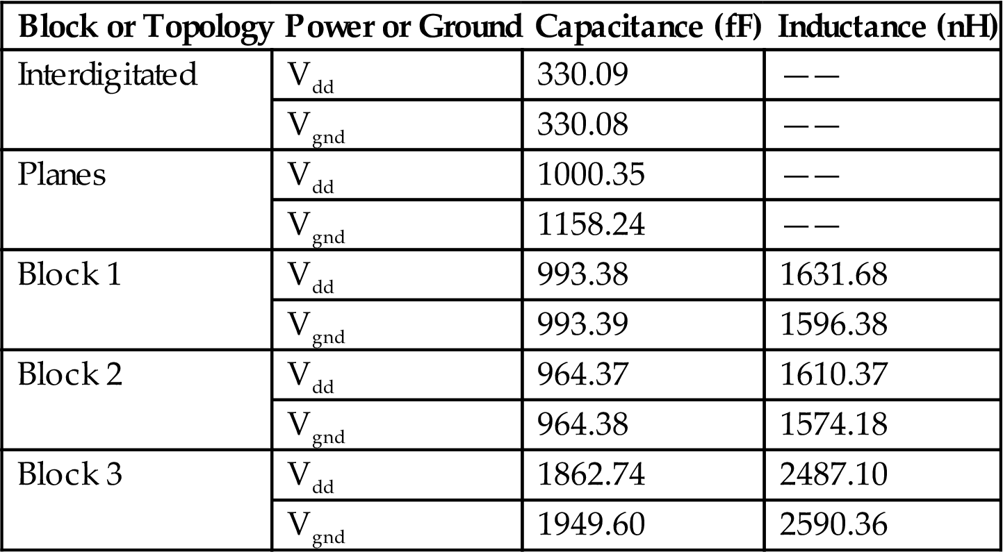
Table 19.6
Capacitance of the Three Different Power Distribution Blocks, Interdigitated, and Power/Ground Planes
| Block or Topology | Power or Ground | Capacitance (fF) | Inductance (nH) |
| Interdigitated | Vdd | 330.09 | —— |
| Vgnd | 330.08 | —— | |
| Planes | Vdd | 1000.35 | —— |
| Vgnd | 1158.24 | —— | |
| Block 1 | Vdd | 993.38 | 1631.68 |
| Vgnd | 993.39 | 1596.38 | |
| Block 2 | Vdd | 964.37 | 1610.37 |
| Vgnd | 964.38 | 1574.18 | |
| Block 3 | Vdd | 1862.74 | 2487.10 |
| Vgnd | 1949.60 | 2590.36 |

The interdigitated power and ground lines in metal 3 are 530 μm long, 15 μm wide, and exhibit a sheet resistance of 0.08 Ω per sheet, producing a 2.83 Ω resistance. Similarly, the metal 2 lines are 500 μm long and 15 μm wide with a sheet resistance of 0.12 Ω per sheet, producing a 4 Ω resistance. Each power and ground line is divided into eight equal RLC π model sections to represent the distributed nature of the on-chip metal lines. An inductance of 1 pH is included with each π model section. Three horizontal pairs (metal 3) of power and ground lines as well as three vertical pairs (metal 2) of power and ground lines are considered for each interdigitated power distribution network on each device plane. The RLC parameters for a single π section of the interdigitated topology also model the dedicated plane topology, but the connections between sections are modified to better characterize the power and ground planes, as illustrated in Fig. 19.21.
The resonant frequency for the three different power distribution networks is determined with and without board level decoupling capacitors and with and without an intentional on-chip load capacitance (separate from the intrinsic capacitance of the power distribution network). The resulting resonant frequency for the three power distribution topologies for the different capacitive configurations is listed in Table 19.7. The resonant frequencies reported in Table 19.7 consider the distributed inductance of the cables, board, wirebonds, and on-chip power distribution network. The on-chip inductance produces the highest resonant frequency, as reported in Table 19.7 for each block. The other three resonant frequencies, from the smallest to the largest, are dependent, respectively, on the cable, board, and wirebond inductances. The presence of a board level decoupling capacitor eliminates all but the highest resonant frequency, the resonance caused by the on-chip inductance.
Table 19.7
Resonant Frequency of the Three Different Power Distribution Networks with and without Board Level Decoupling Capacitors and with and without an On-Chip Load Capacitance
| Block | DecouplingCapacitance (μF) | Extracted Load (fF) | Resonant Frequencies (GHz) |
| Block 1 | none | none | 0.224, 0.447, 0.794, 1.25 |
| 4 | none | 1.25 | |
| none | 638 | 0.199, 0.447, 0.708, 1.25 | |
| 4 | 638 | 1.25 | |
| Block 2 | none | none | 0.223, 0.447, 0.794, 1.78 |
| 4 | none | 1.78 | |
| none | 646 | 0.199, 0.447, 0.708, 1.78 | |
| 4 | 646 | 1.78 | |
| Block 3 | none | none | 0.224, 0.447, 0.794, 1.67 |
| 4 | none | 1.67 | |
| none | 624 | 0.199, 0.447, 0.708, 1.67 | |
| 4 | 624 | 1.67 |

19.3.2 Design Considerations Based on Experimental Results
Based on the experimental results, both increasing the number of TSVs by 50% and utilizing a dedicated power and ground plane lower the power noise. Although the noise is lower with both a greater number of TSVs and dedicated power planes (2% to 14.2% lower noise, as listed in Table 19.8), the power noise is limited by the small series resistance of the 3-D power network as compared with the larger series resistance of the cables and wirebonds, as described in Section 19.3.1.
Table 19.8
Per cent Reduction in Average Noise from the Noisiest Topology (Block 2) to the Least Noisiest Topology (Block 3) as a Function of Bias Voltage on the Current Mirrors
| Power or Ground | DeCap Present | Noisier Block | Quieter Block | Per cent Noise Reduction as Function of Bias Voltage (volts) | |||||
| 0 | 0.25 | 0.5 | 0.75 | 1 | 1.25 | ||||
| Power | No | 2 | 1 | 14.0 | 2.7 | 8.9 | 7.7 | 7.1 | 7.9 |
| 2 | 3 | 14.2 | 2.3 | 10.5 | 8.7 | 12.2 | 10.0 | ||
| 1 | 3 | 0.2 | −0.4 | 1.8 | 1.2 | 5.5 | 2.4 | ||
| Power | Yes | 2 | 1 | 1.2 | 1.2 | 5.2 | 8.3 | 5.6 | 6.6 |
| 2 | 3 | 3.0 | 5.2 | 4.2 | 11.9 | 6.7 | 6.2 | ||
| 1 | 3 | 1.8 | 4.1 | −1.0 | 3.9 | 1.2 | −0.4 | ||
| Ground | No | 2 | 1 | 3.6 | 6.5 | 6.1 | 6.9 | 4.9 | 3.4 |
| 2 | 3 | 6.2 | 6.2 | 7.4 | 9.3 | 7.0 | 4.3 | ||
| 1 | 3 | 2.6 | −0.3 | 1.3 | 2.5 | 2.2 | 0.9 | ||
| Ground | Yes | 2 | 1 | 6.0 | 5.9 | 5.1 | 5.2 | 1.6 | 4.7 |
| 2 | 3 | 8.4 | 7.1 | 6.1 | 7.1 | 4.8 | 7.9 | ||
| 1 | 3 | 2.6 | 1.3 | 1.1 | 2.1 | 3.3 | 3.4 | ||

Two issues in 3-D power distribution networks are considered based on the experimental results: (1) the benefits of the power and ground planes to justify the use of two metallization levels, and (2) the benefits and drawbacks of increased TSV density on area and noise. Addressing (1), the power planes provide an additional reduction of 0.2% to 5.5% in average noise as compared with the fully interdigitated topology. The reduction in average noise is primarily due to the increased capacitance of the power and ground networks, as indicated in Table 19.6. The average noise characteristics of the planes topology can be further improved by increasing the size of the power/ground planes or using multiple metal layers for both power and ground. The use of full planes to deliver current to the load does; however, require significant metal resources and therefore this issue must be considered. In addition, the power planes complicate the design of the signal interconnects, where holes are required in the power/ground planes to pass signals between device planes. For those applications where greater noise reduction is required, additional metallization and design complexity may be justified.
The choice of TSV density provides the greatest reduction in average noise, ranging from 2.7% to 14.0%, as listed in Table 19.8. The additional area penalty when increasing the number of TSVs by 50% from 576 to 864 is 0.68% (1.36% as compared with 2.04%), noting that the area penalty is also dependent on the keep out region, as described in Section 19.3.1. The increased area due to the higher TSV density is small as compared to the large reduction in average noise.
19.4 Summary
The design of a power distribution network for application to 3-D circuits is considerably more complex than the design of a 2-D power network. The primary issues in the design process of a 3-D test circuit and related measurements are summarized as follows:
• The preferable topology of a power distribution network is not dictated by a single design objective but, rather, by the overall 3-D system level requirements, including the availability of I/O pins and number of bonded tiers. This test circuit provides enhanced understanding of topology dependent noise generation and propagation within 3-D power delivery systems.
• A test circuit examining power grid noise in a 3-D integrated stack has been designed, fabricated, and tested. Three topologies to distribute power within a 3-D circuit have been evaluated, and an analysis of the peak noise voltage, voltage range, average noise voltage, and resonant frequency characteristics for both power and ground is discussed.
• Fabrication and vertical bonding were performed by MIT Lincoln Laboratory for a 150 nm, three metal layer SOI process. Three wafers are vertically bonded to form a 3-D stack.
• A noise analysis of three power delivery topologies is described. Calibration circuits for a source follower sense circuit compare the different power delivery topologies as well as the individual 3-D circuits. The effects of the TSV density on the noise profile of a 3-D power delivery network are experimentally characterized.
• A comparison of the peak noise and resonant behavior for each topology with and without board level decoupling capacitors is provided, and suggestions for enhancing the design of the power delivery network are offered.