
This model of skew variations is used to analyze the effects of process variations on various 3-D clock trees. This model is extended to include variations of the horizontal interconnects, as described in Appendix F.
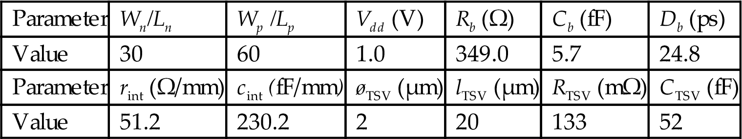
The accuracy of the model is demonstrated through a comparison with Monte Carlo simulations. The structure used for this purpose is an H-tree clock distribution network. This H-tree is placed in a circuit with a total area of 10 mm×10 mm. The circuit is assumed to be manufactured in a 45 nm CMOS technology. The parameters of the transistors and the interconnects are extracted from the PTM 45 nm CMOS and global interconnect models [252] and International Technology Roadmap for Semiconductors (ITRS) [643]. The clock buffers consist of two inverters connected in series. The circuit parameters are listed in Table 17.2. The ratio of the width to the channel length is denoted by Wn/Ln and Wp/Lp for, respectively, the NMOS and PMOS transistors. The interconnect resistance and capacitance per unit length are, respectively, denoted by rint and cint. The physical and electrical characteristics of the TSVs are also listed in Table 17.2 and are based on the data reported in [181,58] (see Chapter 4, Electrical Properties of Through Silicon Vias). The diameter and length of the TSVs are notated, respectively, as øTSV and lTSV.
Table 17.2
Device and Interconnect Parameters of the Target Circuit
| Parameter | Wn/Ln | Wp /Lp | Vdd (V) | Rb (Ω) | Cb (fF) | Db (ps) |
| Value | 30 | 60 | 1.0 | 349.0 | 5.7 | 24.8 |
| Parameter | rint (Ω/mm) | cint (fF/mm) | øTSV (μm) | lTSV (μm) | RTSV (mΩ) | CTSV (fF) |
| Value | 51.2 | 230.2 | 2 | 20 | 133 | 52 |
The variation of the effective channel length of transistors Leff is considered in this comparison, which is the most significant source of device variations [622,633,638,640]. Note that the effects of other sources of process variations are also represented by the circuit illustrated in Fig. 17.6 and described by the analytic model in (17.13)–(17.20). The corresponding nominal Leff, D2D variation ![]() , and WID variation
, and WID variation ![]() are, respectively, 27, 2.2, and 2.7 nm [643]. The resulting variations of Rb, Cb, and Db are listed in Table 17.1, which are obtained as discussed in Section 17.2.1 with an input slew rate of 47, 16, and 6 mV/ps. The mean value and standard deviation are denoted, respectively, by μ and σ. The ratio σ/μ indicates the importance of variations [633]. The Monte Carlo simulation is repeated 1,000 times. As reported in Table 17.1, σ of Rb, Cb, and Db all depend on the input slew rate. Simultaneously considering both the slew rate and the load is therefore necessary when evaluating buffer delay variations.
are, respectively, 27, 2.2, and 2.7 nm [643]. The resulting variations of Rb, Cb, and Db are listed in Table 17.1, which are obtained as discussed in Section 17.2.1 with an input slew rate of 47, 16, and 6 mV/ps. The mean value and standard deviation are denoted, respectively, by μ and σ. The ratio σ/μ indicates the importance of variations [633]. The Monte Carlo simulation is repeated 1,000 times. As reported in Table 17.1, σ of Rb, Cb, and Db all depend on the input slew rate. Simultaneously considering both the slew rate and the load is therefore necessary when evaluating buffer delay variations.
Two H-tree topologies are used to verify the accuracy of the skew variation model. The first topology (multi-via) is illustrated in Fig. 17.5. The second topology (single via) is illustrated in Fig. 17.9. These topologies are compared in the following subsection. The H-tree spans four tiers. The clock source is located at the center of the first tier. There are 128 clock sinks in total, 32 in each tier. The clock buffers, marked with ![]() are inserted following the technique described in [602]. The clock frequency is 1 GHz and the constraint on the input slew rate is 16 mV/ps (the transition time is 5% of the clock period). The number of buffers inserted into the multi-via and single via topologies are, respectively, 168 and 540. Only a few buffers are illustrated in Figs. 17.5 and 17.9 for improved readability. The wire segments between the two buffers are simulated using a standard RC π model.
are inserted following the technique described in [602]. The clock frequency is 1 GHz and the constraint on the input slew rate is 16 mV/ps (the transition time is 5% of the clock period). The number of buffers inserted into the multi-via and single via topologies are, respectively, 168 and 540. Only a few buffers are illustrated in Figs. 17.5 and 17.9 for improved readability. The wire segments between the two buffers are simulated using a standard RC π model.

Both skew variations with uncorrelated (independent) WID variations and correlated WID variations modeled by the multi-level spatial correlation approach are simulated where five levels are assumed (l=5). The error of the skew variation model between any pair of sinks in the target clock tree is below 6%.
17.2.4 Skew Variations in Three-Dimensional Clock Tree Topologies
The skew variation for two types of 3-D global H-trees is investigated in this subsection. The first topology (a multi-via topology) is shown in Fig. 17.5, where the clock source and buffers (except for the buffers at the last level) of a 3-D H-tree are located in a single physical tier (e.g., the first tier). In this topology, the clock signal is propagated to the sinks in other tiers by multiple TSVs. The vertical lines at each leaf correspond to a cluster of TSVs. The second clock tree topology (a single via topology) is illustrated in Fig. 17.9, where a 2-D H-tree is replicated in each tier. The clock signal is propagated by a single via (or a group of TSVs to prevent TSV failure and to lower the resistance of this vertical path), connecting the clock source to each H-tree replica.
To better understand the distribution of skew within these topologies, an intratier (pair of sinks placed in the same tier) and intertier (pair of sinks placed in different tiers) distribution of skew is considered separately. In 3-D H-trees and for intratier paths, the number, size, and location of the buffers along these paths are equal for a single tier since multi-via and single via topologies are both symmetric topologies (at least within the x and y directions). D2D variations in each tier, therefore, affect these clock paths equally. Consequently, according to (17.40), for both the multi-via and single via topologies, only WID variations affect the variation of skew between sinks located on the same tier. For both the single via and multi-via tree topologies, the variation of skew between the buffers located in the same tier exhibits the same behavior as in 2-D circuits.
For a 3-D clock tree, as described by (17.44), if Rin and Cl of each buffer remain unchanged, ![]() between two sinks decreases as the number of nonshared clock buffers (e.g., the buffers after the nu,v buffers shown in Fig. 17.8) decreases. For a 3-D circuit with area A, the side length of each tier is
between two sinks decreases as the number of nonshared clock buffers (e.g., the buffers after the nu,v buffers shown in Fig. 17.8) decreases. For a 3-D circuit with area A, the side length of each tier is ![]() . Consequently, the number of buffers in one tier decreases as L decreases for an increasing number of tiers forming a 3-D circuit. For the single via topology, all of the clock sinks within a tier are connected to the clock source by the same TSV. The length of this TSV and the increasing number of buffers vertically connected to this TSV do not affect the intratier skew. Consequently, for the single via topology, the distribution of skew between clock sinks in the same tier becomes narrower as the number of tiers increases.
. Consequently, the number of buffers in one tier decreases as L decreases for an increasing number of tiers forming a 3-D circuit. For the single via topology, all of the clock sinks within a tier are connected to the clock source by the same TSV. The length of this TSV and the increasing number of buffers vertically connected to this TSV do not affect the intratier skew. Consequently, for the single via topology, the distribution of skew between clock sinks in the same tier becomes narrower as the number of tiers increases.
For the multi-via topology, however, the clock sinks in the same tier connect to different TSVs. As the number of tiers increases, both the number of buffers connecting to a TSV and the length of the TSVs increase. The input slew rate decreases since the load is increasing. As reported in Table 17.1, the delay variations of the buffers after the TSVs increase. Moreover, the load of the buffers driving the TSVs increases. These changes in the topological characteristics increase σd(i), as described by (17.29). This increase, consequently, counteracts and can surmount the decrease in variations due to the fewer clock buffers along the clock paths.
The buffers inserted into the 3-D clock trees are reported in Table 17.3. The number of inserted buffers within one tier in the single via topology is lower than the multi-via topology, which introduces a lower WID skew variation than the multi-via topology. The total number of buffers in a single via topology is, however, much higher than the multi-via topology. The numbers of buffers in each tier for both topologies decreases as the number of tiers increases. The increasing number of buffers connected to TSVs (due to the greater number of tiers) increases σsu,v in the multi-via topology but does not affect σsu,v in the single via topology. Consequently, the decrease in the number of buffers leads to a reduction in skew variation within the same tier for the single via topology, as shown by the (♦) and (■) curves in Fig. 17.10A. Nevertheless, for the multi-via topology, as shown by the Δ and × curves, σsu,v within the same tier changes nonmonotonically with the number of tiers. For the short distance sinks, σs1,2 increases with the number of tiers. As a result, for multi-via 3-D H-trees, simply increasing the number of tiers does not necessarily lower the clock skew. By employing the proposed skew variation model, the number of tiers that produces the lowest skew variation can be determined. Based on this behavior, in a 3-D circuit, if the data related sinks are located mostly within the same tier, the single via topology is more efficient in reducing skew variations and can therefore support a higher clock frequency.
Table 17.3
Number of Buffers Inserted Into the 3-D Clock Trees
| # of Tiers | 1 | 2 | 3 | 4 | 5 | 6 | 7 | 8 | 9 | 10 |
| Multi-via | 981 | 588 | 558 | 264 | 264 | 242 | 234 | 138 | 134 | 134 |
| Single via (per tier) | 981 | 460 | 231 | 199 | 199 | 177 | 169 | 105 | 101 | 101 |
| Single via (total) | 981 | 920 | 924 | 995 | 995 | 1062 | 1183 | 840 | 909 | 1010 |


A different behavior is observed when considering intertier skew. As described by (17.40) through (17.42), when the target clock sinks are located in different tiers, the corresponding clock skew is also affected by D2D variations. For the single via topology, the skew variation for the intertier pairs of sinks remains approximately the same irrespective of the tiers to which the sinks belong. This behavior occurs since the paths to the sinks located in different tiers do not share any common segments (see Fig. 17.9). When the number of tiers is greater than two, the skew variation decreases as the number of tiers increases, as also shown in Fig. 17.10B. Since the paths lay in different tiers, according to (17.42), the effect of D2D variations on the 3-D single via topology is much greater than in planar H-trees.
The skew variation under the multi-via topology varies significantly from the single via topology, as illustrated in Fig. 17.10B. The skew variation between tiers depends upon the location of the related sinks. According to (17.40)–(17.42), the effects of D2D variations increase as the number of buffers located in different tiers increases. For the multi-via topology, all of the clock paths preceding the TSVs are in the first tier. The effects of D2D variations on the multi-via topology, therefore, are much smaller than the single via topology, as shown in Fig. 17.10B. Nevertheless, the skew variation of the multi-via topology changes nonmonotonically with the number of tiers. In a 3-D circuit, if the data related sinks are widely distributed on several tiers, the multi-via topology is more efficient in reducing skew variations and can therefore support a higher clock frequency.
These results indicate that the performance improvement in a 3-D clock network depends significantly on the distribution of the sinks (and, consequently, the clock paths) among the tiers. When the data related sinks are distributed on different tiers, the skew of the single via 3-D clock trees is affected more by process variations than a corresponding 2-D clock tree. This behavior is consistent with the conclusions made in Section 17.1 for data paths in 3-D circuits. The effects of process variations on 3-D clock distribution networks can be mitigated in this case by employing a multi-via topology. This topology can better exploit the traits of vertical integration (i.e., shorter wires) to significantly increase the operating frequency.
Based on these observations, a hybrid H-tree topology (multi-group topology) combining the advantages of both the single and multi-via topologies exhibits the lowest clock skew variability. The multi-group topology is illustrated in Fig. 17.11. The key concept is that the m tiers forming a 3-D circuit are divided into Q groups of “data related tiers.” The data related tiers are the physical tiers containing data related registers. The ith group of data related tiers consists of hi (≤m) physical tiers. The clock signal is distributed within these hi tiers by a multi-via topology.

An example of this H-tree topology is illustrated in Fig. 17.11. This H-tree includes two groups of data related tiers (Q=2). The first group spans three tiers (h1=3), and the second group spans two physical tiers (h2=2). The buffers contained in each group of data related tiers are denoted by empty “triangles” and “dots.” The TSVs connecting these buffers are called “sink TSVs.” The root of the multi-via topologies is connected with a “root TSV” (or a cluster of TSVs), as illustrated by the segment at the center of the tiers.
For a 3-D circuit, if all the data related clock sinks cannot be located within the same tier but in adjacent tiers, the multi-group topology is more efficient in reducing skew variations than the other topologies. Compared with the single via topology, using Q instead of m H-trees, the multi-group topology significantly reduces skew variations between data related tiers. As compared with the multi-via topology, the multi-group topology requires fewer buffers connected to the sink TSVs than buffers connected to the TSVs of the multi-via topology. Both skew variations within a single tier and skew variations between data related tiers are therefore reduced.
To quantify the ability of a multi-group tree to reduce skew variations among the clock sinks, a 3-D circuit with eight tiers is evaluated. Two variants of the multi-group topology are considered, including two groups (hybrid 2, Q=2, hi=4) and four groups (hybrid 4, Q=4, hi=2) of data related tiers. Simulation results are shown in Fig. 17.12.

In Fig. 17.12, skews s1,2 and s1,3 (illustrated in Fig. 17.5B) and s1,6 and s1,7 (illustrated in Fig. 17.11) are depicted exhibiting skew variations between the nearest and farthest sinks. The results, based on independent and multi-level correlated WID variations, are denoted, respectively, by (I) and (II). σs1,2 and σs1,3 produced by the multi-group topology are lower than the multi-via topology and decrease as the number of sub-H-trees increases. For the topology with four sub-H-trees (hybrid 4), s1,2(I), s1,3(I), s1,2(II), and s1,3(II) are reduced, respectively, by 55%, 23%, 44%, and 10% as compared with the multi-via topology. Although σs1,3 within the same tier of the multi-group topology is greater (4% for hybrid 4) than the single via topology, the intertier skews σs1,6 and σs1,7 within a group of data related tiers of the multi-group topology are significantly reduced, as shown in Fig. 17.12B. This reduction is also greater than the multi-via topology. The number of sub-H-trees within a multi-group 3-D topology is determined by the distribution of the data related sinks. Consequently, if the data related sinks are located in adjacent tiers of a 3-D circuit, the multi-group 3-D clock tree topology is more efficient in reducing skew variations than both the single and multi-via topologies.
17.3 Effect of Process and Power Supply Variations on Three-Dimensional Clock Distribution Networks
D2D variations due to the multi-tier nature of 3-D circuits increase the variation in the delay of intertier paths, as shown in Section 17.1. This greater variation in delay manifests as larger timing uncertainty in clock distribution networks that span several tiers. A greater timing uncertainty hinders the management of skew which can in turn degrade the performance of a 3-D clock distribution network, as discussed in Section 17.2. Similar to the situation where different D2D variations are assumed among the tiers of a 3-D system, each tier experiences disparate power supply noise, as discussed in Chapter 18, Power Delivery for Three-Dimensional ICs.
Power supply noise in a clock distribution network adds to the timing uncertainty, although differently than process variations. Power supply noise can produce clock jitter. Clock jitter can occur in three different ways: period jitter, cycle-to-cycle jitter, and phase jitter (or time interval error) [645]. Period jitter is the difference between the measured clock period and the ideal period, which is the most explicit form of clock jitter within a circuit. Cycle-to-cycle jitter is the variation in clock period between adjacent clock periods over a random sample of cycles [646]. For a random number of clock cycles, phase jitter is the departure in phase of a specific edge from the mean phase [646].
The jitter is produced by a phase locked loop (PLL) driving a clock distribution network. PLL jitter can be mitigated by careful design of the PLL [647]. Furthermore, power supply noise affects the clock buffers used within the distribution network, leading to higher clock jitter [648]. This increase in jitter within planar clock distribution networks is discussed in [649,650]. A similar analysis cannot however be easily applied to 3-D circuits due to the disparate power supply noise that buffers within different tiers can experience [651]. Moreover, clock distribution networks are simultaneously affected by process variations and power supply noise. Consequently, the combined effects of process variations and power supply noise on a multi-tier 3-D clock distribution network are discussed in this section where both theoretical and practical design issues are reviewed. A term introduced in [652] to describe both skew and jitter, skitter, is utilized throughout this section.
A methodology to determine the delay variation of a buffer stage under process and power supply variations is presented in the following subsection. With a statistical description of the delay of a clock buffer, a model that describes the combined effects of clock skew and jitter of 3-D clock trees is presented in Section 17.3.2. Based on this model, several tradeoffs among the skitter, power of the clock network, and allocation of clock buffers among tiers are considered in Section 17.3.3. Related design guidelines to mitigate skitter and lower the complexity are presented in Section 17.3.4.
17.3.1 Delay Variation of Buffer Stages
The distribution of the delay of a buffer stage is modeled in this subsection. The delay of a buffer stage d consists of the delay of the buffer db and the interconnect (horizontal wire and/or through silicon via) dI. The variation of d is modeled in this subsection as a random variable affected by both process variations and power supply noise.
Since the variation of parameters due to process variations is typically within a small range, the delay of a buffer stage considering parameter variations can be approximated by a first order Taylor series expansion [637]
(17.48)
The input slew rate of this buffer stage is denoted by tr. The capacitive load at the output of the buffer and wire is denoted, respectively, by Clb and Clw. The nominal delay is ![]() and the subscript “0” denotes the partial derivative assuming nominal parameters. The set of parameters affected by process variations is denoted by
and the subscript “0” denotes the partial derivative assuming nominal parameters. The set of parameters affected by process variations is denoted by ![]() . Each parameter is modeled as a random variable. For instance, if the variation of the channel length of three buffers is considered,
. Each parameter is modeled as a random variable. For instance, if the variation of the channel length of three buffers is considered, ![]() is {Lb,1, Lb,2, Lb,3}. The variation of a parameter
is {Lb,1, Lb,2, Lb,3}. The variation of a parameter ![]() consists of WID and D2D variations,
consists of WID and D2D variations,
(17.49)
where ![]() is constant among the buffers and interconnects within the same die, while
is constant among the buffers and interconnects within the same die, while ![]() varies among the components within the same die [638]. The individual partial derivatives in (17.48) are
varies among the components within the same die [638]. The individual partial derivatives in (17.48) are
(17.50)
The partial derivatives in (17.50) are determined from the expression for ![]() and
and ![]() . The expression of
. The expression of ![]() is obtained through analytic formulas [653] or an adjoint sensitivity analysis with SPICE-based simulations [637]. To achieve higher accuracy, the latter is used. For horizontal wires, the expression of
is obtained through analytic formulas [653] or an adjoint sensitivity analysis with SPICE-based simulations [637]. To achieve higher accuracy, the latter is used. For horizontal wires, the expression of ![]() is based on the RLC interconnect model described in [654,655].
is based on the RLC interconnect model described in [654,655].
The variations introduced by the TSVs are discussed in [656,657], where TSV stress induced delay variations of buffers are modeled. In this chapter, the keep out zone around the TSVs is assumed to be sufficiently large (≤10 μm [657,658]) to mitigate the effects of TSV stress. Consequently, the TSVs are modeled as RLC wires with different electrical characteristics than the horizontal interconnects
In addition to process variations, the power noise also affects the buffer delay. The supply voltage ![]() is affected by the power noise v,
is affected by the power noise v, ![]() , where Vdd0 is the nominal power supply voltage of the circuit. As the power noise contains several components across a large range of frequencies, the focus of this section is on the frequency noise component due to the capacitance of the on-chip power distribution network and the inductance of the package. This noise is typically between tens and several hundred MHz (e.g., 400 MHz) [649].
, where Vdd0 is the nominal power supply voltage of the circuit. As the power noise contains several components across a large range of frequencies, the focus of this section is on the frequency noise component due to the capacitance of the on-chip power distribution network and the inductance of the package. This noise is typically between tens and several hundred MHz (e.g., 400 MHz) [649].
This noise is modeled as a sinusoidal waveform where the amplitude of the waveform is the worst case noise observed in the clock network. Assuming a clock edge arrives at the source of a clock path at time zero, tj is the time when this clock edge arrives at buffer j. The supply noise at buffer j at time tj is
(17.51)
(17.52)
The clock frequency is much higher than the resonant noise frequency, and the clock path delay is typically lower than the period of the resonant noise. Due to the significant voltage drop, the first period of the resonant noise causes the greatest clock jitter [649]. Consequently, to investigate the effects of the worst case power noise on clock distribution networks, (17.51) is approximated by an undamped sinusoidal waveform [649]
(17.53)
According to (17.48) and (17.52), di, tj, and v(tj) are all random variables. Since ![]() is low as compared with
is low as compared with ![]() , v(tj) can also be approximated by a first order Taylor series expansion,
, v(tj) can also be approximated by a first order Taylor series expansion,
(17.54)
(17.55)
The amplitude Vn and frequency fn are determined by the switching current and the circuit characteristics. The initial phase ϕ is the phase of the resonant noise when the clock edge arrives at the source of the clock path.
In 3-D circuits, the current dissipated by the tiers can differ due to the different number and size of the devices. The amplitude and frequency of the resonant supply noise change with the current within different tiers. To demonstrate this behavior, a 1-D model of a power distribution network for a three tier circuit, shown in Fig. 17.13, is considered under different switching scenarios. Four cases of switching current are considered for this power network, which are listed in Table 17.4. The pulse width and transition times of the switching current are both 1 ns. The resulting Vn and fn are depicted in Fig. 17.14. As illustrated in this figure, different current distributions introduce a nonnegligible difference in Vn among tiers ΔVn. The IR drop and resonance impedances among the tiers both contribute to this ΔVn. The resonant frequency is similar among tiers (Δfn≤3 MHz) and does not change significantly with the current.

Table 17.4
Four Scenarios of Switching Current Within a Three Tier Circuit
| Case | cur1 | cur2 | cur3 | cur4 |
| I1 (A) | 0 | 10 | 20 | 40 |
| I2 (A) | 20 | 20 | 20 | 20 |
| I3 (A) | 40 | 30 | 20 | 0 |


The electrical characteristics of the TSVs depend upon the manufacturing technology [201,181]. The change of the power noise with the total resistance of the TSVs (Rtsv) is illustrated in Fig. 17.15. In this figure, the amplitude and frequency of the overall supply noise are denoted, respectively, by V3–V1 and f3–f1. The DC IR drop is denoted by V3_dc–V1_dc. Since the resonant noise is stimulated by a current pulse, the effect of the IR drop is also included in V3–V1.

A larger RTSV introduces a higher IR drop in the first and second tiers. In the third tier, the DC IR drop is not affected by RTSV since this tier is directly connected to the package (see Fig. 17.13). Nevertheless, a higher RTSV decreases the quality factor (Q factor) of the resonant circuit, which decreases the amplitude of the resonance. Consequently, Vn in the third tier decreases with RTSV. In the first and second tiers, Vn is determined by both the resonance and the IR drop. Consequently, V2 and V1 increase with RTSV due to the significantly higher IR drop. Nevertheless, the increase in V2 and V1 is not as high as the increase in the DC IR drop due to the lower Q factor.
The resonant noise for different number of tiers in a 3-D IC is plotted in Fig. 17.16. The switching current and on-die capacitance are assumed identical for all tiers. As shown in Fig. 17.16, ΔVn between the bottom and top tiers increases with the number of tiers. As more dies are vertically stacked, the difference in resonant noise among tiers increases.

According to (17.48), the delay variation Δd is also affected by the input slew ![]() , which is determined by the previous buffer stage. Considering the effects of
, which is determined by the previous buffer stage. Considering the effects of ![]() and
and ![]() on
on ![]() the delay variation of the jth buffer stage is modeled as
the delay variation of the jth buffer stage is modeled as
(17.56)
The set of statistical parameters of the jth buffer stage is denoted by ![]() , which is a subset of the entire parameter set,
, which is a subset of the entire parameter set, ![]() . The input slew of the jth buffer stage
. The input slew of the jth buffer stage ![]() is determined similarly to (17.56),
is determined similarly to (17.56),
(17.57)
Substituting (17.55) and (17.57) into (17.56), ![]() can be recursively determined considering both process variations and power noise. The coefficients in (17.56) and (17.57) are obtained through an adjoint sensitivity analysis, as previously mentioned. The resulting expression, (17.56), determines the skitter, as described in the following subsection.
can be recursively determined considering both process variations and power noise. The coefficients in (17.56) and (17.57) are obtained through an adjoint sensitivity analysis, as previously mentioned. The resulting expression, (17.56), determines the skitter, as described in the following subsection.
17.3.2 Model of Skitter in Three-Dimensional Clock Trees
The definitions of clock skew, period jitter, and skitter are illustrated in Fig. 17.17. The clock signal is fed into the 3-D clock tree from the primary clock driver. Two flip flops are driven by this clock signal, denoted, respectively, as FF1 and FF2. The waveforms, clk1 and clk2, shown in Fig. 17.17B correspond to the clock signal driving, respectively, FF1 and FF2. The time when the first rising edge in Fig. 17.17B arrives at the clock input is defined as the origin. The time when this clock edge arrives at FF1 and FF2 is, respectively, denoted by t1 and t2. The arrival time of the next rising edge is t′1 and t′2. The number of buffers from the clock input to FF1 and FF2 is denoted, respectively, by n1+n2 and n3+n4. The skew between the first edge of clk1 and clk2 is S1,2. The clock period after the first edge for FF1 and FF2 are, respectively, T1 and T2. The clock period is Tclk. The corresponding period jitter is J1=T1−Tclk and J2=T2−Tclk.

Assuming the data is transferred from FF1 to FF2 within one clock cycle, T1,2 is the time interval that determines the highest clock frequency supported by the circuit. The setup time requirement needs to be satisfied for the system to operate correctly [577,645]. The setup time slack notated as slacksetup is defined as
(17.58)
(17.59)
where ![]() denotes the longest data transfer time from FF1 to FF2. The setup time for FF2 is
denotes the longest data transfer time from FF1 to FF2. The setup time for FF2 is ![]() . Consequently, the variation of
. Consequently, the variation of ![]() is affected by the variation of
is affected by the variation of ![]() , called “setup skitter” and notated as
, called “setup skitter” and notated as ![]() ,
,
(17.60)
To avoid setup time violations, ![]() is required under all operating conditions.
is required under all operating conditions.
According to (17.52) and (17.60), skitter ![]() is the linear combination of the delay of the buffer stages,
is the linear combination of the delay of the buffer stages,
(17.61)
(17.62)
(17.63)
where ![]() is the delay of the kth buffer stage along the path to FF2 for the second clock edge. The mean skitter
is the delay of the kth buffer stage along the path to FF2 for the second clock edge. The mean skitter ![]() is the mean delay of all of the buffer stages considering the mean voltage supply noise (without process variations). Substituting (17.56) into (17.63), the partial derivative
is the mean delay of all of the buffer stages considering the mean voltage supply noise (without process variations). Substituting (17.56) into (17.63), the partial derivative ![]() is obtained. Consequently, skitter J1,2 is approximated by a first order Taylor series expansion. Assuming all of the parameters are characterized by a Gaussian distribution, ΔJ1,2 can also be approximated by a Gaussian distribution,
is obtained. Consequently, skitter J1,2 is approximated by a first order Taylor series expansion. Assuming all of the parameters are characterized by a Gaussian distribution, ΔJ1,2 can also be approximated by a Gaussian distribution,
(17.64)
(17.65)
where ![]() denotes the covariance between two parameters. Assuming D2D variations are independent from WID variations [632,637],
denotes the covariance between two parameters. Assuming D2D variations are independent from WID variations [632,637], ![]() . The covariance between the two parameters is determined according to the tiers to which these parameters are related and the spatial correlation between these parameters,
. The covariance between the two parameters is determined according to the tiers to which these parameters are related and the spatial correlation between these parameters,
(17.66a-b)
where the WID covariance ![]() is determined by the spatial correlation between parameters p and q within the same tier. Statistically, the devices (and wires) close to each other exhibit a higher correlation than those devices far from each other. This spatial correlation can be obtained from fabricated wafers [659] or through a spatial correlation model [637,660].
is determined by the spatial correlation between parameters p and q within the same tier. Statistically, the devices (and wires) close to each other exhibit a higher correlation than those devices far from each other. This spatial correlation can be obtained from fabricated wafers [659] or through a spatial correlation model [637,660].
As shown in (17.65) and (17.66), the variance of the setup skitter ![]() depends on the covariance between the process induced parameters. In 2-D circuits, the change of cov(p,q) is primarily determined by cov(p,q)WID since the parameters are affected by the same D2D variations. The distribution of the clock paths therefore only affects
depends on the covariance between the process induced parameters. In 2-D circuits, the change of cov(p,q) is primarily determined by cov(p,q)WID since the parameters are affected by the same D2D variations. The distribution of the clock paths therefore only affects ![]() by changing the WID covariance. In 3-D circuits, however, D2D variations vary among tiers, and the WID covariance among tiers is zero. Consequently, the distribution of the clock paths affects the skitter variation in a highly complicated manner.
by changing the WID covariance. In 3-D circuits, however, D2D variations vary among tiers, and the WID covariance among tiers is zero. Consequently, the distribution of the clock paths affects the skitter variation in a highly complicated manner.
In addition to the setup time slack, the hold time slack also significantly affects circuit performance. The hold time violation can also cause the failure of the entire system [645]. Moreover, this failure cannot be removed by lowering the system wide clock frequency. As illustrated in Fig. 17.17B, the hold time slack is modeled as
(17.67)
where ![]() is the hold time requirement. The “hold skitter” affecting
is the hold time requirement. The “hold skitter” affecting ![]() is determined by
is determined by ![]() , which is the skew between clk1 and clk2. Note that
, which is the skew between clk1 and clk2. Note that ![]() is affected by both process variations and power noise.
is affected by both process variations and power noise.
To correctly latch the data in FF2, ![]() is required to avoid hold time violations under any operating condition. From Fig. 17.17B, S1,2 is
is required to avoid hold time violations under any operating condition. From Fig. 17.17B, S1,2 is
(17.68)
Similar to (17.52) and (17.65), the distribution of ![]() can be modeled as
can be modeled as
(17.69)
(17.70)
where the partial derivatives are obtained similarly to the coefficients in (17.63). As shown by (17.48)–(17.70), both the setup and hold time violations are simultaneously affected by process variations and power noise. This effect and the accuracy of this model are discussed in the following subsection.
17.3.3 Skitter Related Tradeoffs in Three-Dimensional ICs
The variation of skitter for diverse characteristics of a clock distribution network is discussed in this subsection. The number and size of the buffers change with the number of tiers spanned by the clock networks which also affects the dissipated power. The related tradeoffs are discussed in Section 17.3.3.1. The change in skitter as a function of the phase and magnitude of the power noise frequency is summarized in Section 17.3.3.2.
The electrical parameters of the transistors are based on a 32 nm PTM model [252]. The parameters of the interconnects are based on an Intel 32 nm interconnect technology [649]. The parameters of the TSVs are based on data from [181]. Both the horizontal wires and TSVs are modeled by π segments in SPICE-based simulations. The variation aware model of skitter is based on Matlab. All of the simulations are performed in a Scientific Linux server (Intel Xeon 2.67 GHz, 24 cores, 24 GB memory).
The variations considered in the simulations are listed in Table 17.5. The D2D and WID ΔLb are extracted based on ITRS data [661]. The wire variations and ΔVth are based on [637]. The variations of the TSVs are based on [656]. Note that other sources of variations can also be described by this modeling approach. For example, the TSV stress induced delay variation in [657] can be included. In this case, the distribution of dB in (17.48) is based on the distance between the buffer and the TSVs and the stress induced buffer delay.
Table 17.5
Variation of Devices, Horizontal Wires, and TSVs
| Parameters | Nominal | 3σ (D2D) | 3σ (WID) |
| Channel length (nm) | 32 | 1.5 | 2.5 |
| Threshold voltage (mV) | 242 | 24.2 | 24.2 |
| Wire width (nm) | 225 | 22.5 | 11.3 |
| Wire height (nm) | 388 | 19.4 | 9.7 |
| ILD thickness (nm) | 252 | 18.9 | 9.5 |
| TSV resistance (mΩ) | 133 | 39.9 | 39.9 |
| TSV capacitance (fF) | 52 | 15.6 | 15.6 |

17.3.3.1 Skitter versus length of clock paths, number of tiers, and power dissipation
The change in setup skitter with the length of the clock paths is the topic of this subsection. The length ranges from 0.5 to 12.5 mm within two and three tier circuits. Buffers are inserted to produce a 10% Tclk input slew for the next stage. To emphasize the relation between skitter and the length of the clock paths, all tiers are assumed to experience similar supply noise (Vn=90 mv, fn=400 MHz, and ϕ=270° [649]). Each pair of paths is distributed across different tiers, as shown in Fig. 17.17A. The resulting ![]() and
and ![]() are illustrated in Fig. 17.18, where the suffixes “2” and “3” denote the results for, respectively, the two and three tier circuits.
are illustrated in Fig. 17.18, where the suffixes “2” and “3” denote the results for, respectively, the two and three tier circuits.

The results from SPICE-based Monte Carlo simulations and the semi-analytic model (labeled as (m)) are both depicted in Fig. 17.18. As shown in this figure, both ![]() and
and ![]() deteriorate with longer clock paths. This behavior is described by the model and exhibits reasonable accuracy. The error of the model is below 11% for
deteriorate with longer clock paths. This behavior is described by the model and exhibits reasonable accuracy. The error of the model is below 11% for ![]() and below 12% for
and below 12% for ![]() . Not surprisingly, long clock paths introduce high skitter in 3-D clock trees. Consequently, both the mean and standard deviation of the setup skitter increase with the length of the clock paths.
. Not surprisingly, long clock paths introduce high skitter in 3-D clock trees. Consequently, both the mean and standard deviation of the setup skitter increase with the length of the clock paths.
The skitter has been evaluated for no TSV variations, 5% TSV variations (σ/µ=5%), and 15% TSV variations. The difference in ![]() among these three cases is around 1 ps for all of the clock paths. This situation shows that TSV variations are a second order effect, consistent with the results reported in [656].
among these three cases is around 1 ps for all of the clock paths. This situation shows that TSV variations are a second order effect, consistent with the results reported in [656].
In addition to the length of the clock paths, the number of tiers spanned by these paths determines the skitter of the clock distribution network. Due to the different switching currents in power supply networks and the vertical resistance of the P/G TSVs among tiers, the devices in different tiers are subjected to different ΔVn, as shown in Figs. 17.14 and 17.15. The tier closer to the P/G pads experiences a lower power noise, as also discussed in Chapter 18, Power Delivery for Three-Dimensional ICs.
Clock paths spanning two tiers with 20 buffers (n1+n2=n3+n4=20, see Fig. 17.17A) are considered as an example. The clock source is located on tier 2. The total length of each path is 5 mm. The initial phase ϕ (270°) and frequency fn (400 MHz) are assumed to be the same for both tiers. Two distributions of clock paths are discussed: (A) n1=n2=n3=n4=10 and (B) n1=n3=15, n2=n4=5. Distribution (A) denotes equally divided 3-D clock paths. In distribution (B), the longest segment of the clock paths is placed in tier 2. To depict the accuracy of the model, the simulation results of the setup skitter J1,2 for Vn1=90 mV and different Vn2 are shown in Fig. 17.19. As noted in this figure, ![]() changes significantly with Vn2 while
changes significantly with Vn2 while ![]() varies only slightly with Vn2.
varies only slightly with Vn2.

The change in setup skitter J1,2 with (Vn2, Vn1) is illustrated in Fig. 17.20. As shown in Figs. 17.20A and B, for distribution (A), μJ1,2 increases significantly with both Vn2 and Vn1, since higher supply noise introduces greater period jitter. The clock paths of (A) are equally distributed among the tiers. μJ1,2 is therefore similarly affected by Vn1 and Vn2. For distribution (B), however, the situation is different. As shown in Figs. 17.20C and D, μJ1,2 is primarily determined by Vn2 since the longest segment of the clock paths in (B) is placed in tier 2. Consequently, for unequally distributed clock paths, the mean skitter is mainly determined by the tier containing the longest part of the clock paths.

As shown in Figs. 17.20A and B, assuming Vn1=0.09 mV, distribution (A) produces higher μJ1,2 than (B) for different Vn2. This difference in μJ1,2 increases with ΔVn (ΔVn=Vn1−Vn2), from 1% to 42% of μJA. The reason for this significant difference is that the majority of the buffers in (B) is located in tier 2, which is more sensitive to Vn2. More generally, assuming Vn1>Vn2, the mean skitter of (B) is always lower than (A).
Consequently, the distribution of the clock paths in 3-D ICs significantly affects the mean skitter due to the different Vn among tiers. However, in 2-D circuits, this mean skitter does not vary significantly with the distribution of clock paths due to the global resonant noise at low frequencies [662]. The standard deviation σJ1,2 of (A) and (B) is illustrated, respectively, in Figs. 17.20E and F. Similar to μJ1,2, σJ1,2 also increases with Vn1 and Vn2. Nevertheless, ΔσJ1,2 is relatively low as compared with ΔμJ1,2.
Alternatively, the mean value of the hold skitter S1,2 is relatively low (≤0.5 ps) since the two clock paths have the same number, size, and distribution of buffers. Nevertheless, σS1,2 is nonnegligible for both distributions (A) and (B), as illustrated, respectively, in Figs. 17.21A and B. Similar to σJ1,2, σS1,2 increases with Vn1 and Vn2 but ΔσS1,2 is lower than 1.5 ps. These results demonstrate that the standard deviation of the setup and hold skitter increases with the amplitude of the resonant power noise.

The power consumed by the clock distribution networks constitutes a significant portion of the total power consumed by a complex integrated circuit [645]. Clock skitter also depends on the traits of the buffers, which in turn affect the power of the clock network. This power is evaluated under different constraints on the skitter. A pair of clock paths with a length of 5 mm is evaluated. These paths are both equally distributed across two tiers, where Vn1=0.09 volts and Vn2=0.08 volts. The skitter and power are determined from Monte Carlo simulations. A different number (14 to 40) and size (Wn) of the clock buffers are inserted along the clock paths.
Considering the Gaussian distribution of the setup skitter J1,2 in (17.64), J1,2 falls into the range [μJ1,2−3σJ1,2, μJ1,2+3σJ1,2] with a probability of 99.7%. Within this range, max(J1,2) indicates the worst (maximum) skitter. For improved readability the absolute value of max(J1,2) is shown, where max(J1,2)=|μJ1,2|+3σJ1,2. The total power consumption under different constraints on max(J1,2) for these clock paths is illustrated in Fig. 17.22. The shaded area depicts inferior buffer solutions. Point A denotes the lowest skitter that can be obtained for this example circuit. In the unshaded area, the skitter decreases as the buffer size and power increase. For the same constraint in skitter, those clock paths with fewer buffers are more power efficient.

As shown within the unshaded area, the clock paths with fewer buffers produce lower skitter. For the clock paths with 14 buffers, as the constraint becomes lower than 68 ps, significant power is required. For example, to decrease the max(J1,2) from 68 to 58 ps (15% improvement), the buffer size is increased from 4 to 10 μm. The resulting power consumption increases from 6.9 to 14.4 mW (a 109% increase). Consequently, pursuing extreme constraints on clock skitter dissipates high power.
17.3.3.2 Skitter versus phase and frequency of the power supply noise
Another parameter that skitter depends upon is the phase difference between the clock signal and the power supply noise. Assuming that the phase difference is the same between the two tiers, meaning that ϕ1=ϕ2, the change in J1,2 and S1,2 with phase is illustrated in Fig. 17.23 where Vn1=0.09 volts and Vn2=0.07 volts.

As shown in Figs. 17.23A and B, the difference in ϕ produces a significant change not only in μJ1,2 but also in σJ1,2. For instance, the highest σJ1,2 is 41% greater than the lowest σJ1,2 for distribution (A) (see Fig. 17.23B). The worst case μJ1,2 occurs when ϕ1 and ϕ2 are both approximately 270°, similar to 2-D circuits [649]. The worst σJ1,2, however, occurs when ϕ≈205°. Therefore, if the initial phase is not 270°, the skitter can be high due to the high σJ1,2. The difference in σJ1,2 is low between distributions (A) and (B) since, in either case, the clock path to FF1 and FF2 is the same.
The behavior of the hold skitter is different. The effect of ϕ1 and ϕ2, on S1,2 is shown in Fig. 17.23C. Due to the similarity between the two clock paths, the resulting S1,2 is relatively low. The standard deviation, however, is significantly affected by ϕ. As illustrated in Figs. 17.23B and C, the change of σS1,2 is similar to σJ1,2. Consequently, both for setup and hold skitter, σ changes considerably with the phase of the power supply noise. The highest σ and μ of the skitter do not occur at the same initial phase of the supply noise.
Considering the clock paths and waveforms shown in Fig. 17.17, ϕ is the time when the first clock edge arrives at the input of the clock paths. The worst case σ can be obtained by traversing all possible ϕ. Due to the excessive time required for Monte Carlo simulations, this model is highly efficient in determining the worst case skitter and the corresponding ϕ for multi-tier circuits, as compared with Monte Carlo simulations.
As the effect of the noise phase can be significant both for setup and hold skitter, several techniques, such as RC filtered buffers and “stacked” phase-shifted buffers [663], have been proposed to shift the ϕ seen by the clock paths. In 3-D clock distribution networks, these techniques can be applied to a portion of the clock paths in a different tier to increase Δϕ among the tiers. The change in σJ1,2 versus the shifted (ϕ1=ϕ2) for distribution (A) is shown in Figs. 17.24A and B. As shown in Fig. 17.24B, the dashed line depicts σJ1,2 for ϕ1=ϕ2, which denotes the skitter without phase shifting. As shown by the arrow, the highest σJ1,2 decreases with Δϕ=ϕ2−ϕ1. In this case, since ϕ2 and ϕ1 are not simultaneously equal to 270°, the worst case μJ1,2 also decreases.

In Fig. 17.24C, however, σJ1,2 of distribution (B) depends strongly on ϕ2. This behavior occurs since σJ1,2 is dominated by the supply noise in the second tier. In this case, shifting ϕ among tiers provides less than a 1.5 ps decrease in σJ1,2, as shown by the dashed line with arrows. Thus, for equally distributed clock paths across 3-D ICs, the worst case skitter can be decreased by shifting ϕ among those tiers with phase-shifted clock distribution networks.
Note that the proper Δϕ is determined by traversing all of the combinations of ϕ in different tiers. The number of combinations increases exponentially with the number of tiers, requiring a large number of simulations. This unified model provides a highly efficient way to determine a valid shift in ϕ to decrease skitter in multi-tier circuits.
In addition to phase. the frequency of the power supply noise also affects the skitter. This frequency is usually considered to be the same among tiers, as shown in Figs. 17.14 and 17.15. The frequency fn is varied to evaluate the change in skitter with the frequency of the supply noise. The amplitude Vn and phase ϕ are assumed to be the same among tiers, where Vn1=Vn2=90 mV and ϕ1=ϕ2=270°. The simulation results are illustrated in Fig. 17.25.

Similar to the effects of Vn, fn greatly affects μJ1,2. For instance, μJ1,2 increases with fn by up to 70% for distribution (B). The variation of skitter, however, decreases with fn. The resulting ΔσJ1,2 and ΔσS1,2 reach 15% for both distributions (A) and (B). This behavior is due to the lower voltage seen by the clock buffers when the clock propagates along the path. The change of μd and σd for the delay of two serial inverters (a clock buffer) is illustrated in Fig. 17.26A. Both μd and σd decrease with Vdd. As shown in Fig. 17.26A, assume that the clock edge with the worst case σJ arrives at the input of the clock path at t0. When fn increases from fn1 to fn2, the propagation time of this edge decreases from t1 to t2 and the supply voltage within this duration increases. This higher supply voltage introduces lower σ in the buffer delay, which lowers σJ1,2 and σS1,2, see (17.65) and (17.70). Consequently, the mean setup skitter increases significantly with the frequency of the power noise, while both σJ1,2 and σS1,2 decrease with this frequency.

As shown in Fig. 17.25, the statistical model for skitter is reasonably accurate as compared with SPICE-based simulations for different frequencies of the power noise. For the worst case μJ1,2 (σJ1,2) shown in Fig. 17.25, the error is, respectively, −11% (−12%), −7% (−10%), −8% (−4%), and −10% (−9%). Since σJ1,2 varies with the power noise, process variations and power noise need to be simultaneously modeled to correctly characterize the clock delay uncertainty. The difference in mean skitter varies by up to 60% due to the different Vn among tiers. σJ1,2 can vary by up to 51% due to the different ϕ (see Figs. 17.23B and C). Decreasing the variations as well as the mean skitter therefore improves the robustness of 3-D clock distribution networks.
17.3.4 Effect of Skitter on Synthesized Clock Trees
A set of guidelines is provided to support the design of robust 3-D clock distribution networks. The objective of these guidelines is to decrease skitter in 3-D circuits.
Guideline 1: Given the freedom to choose which tiers the clock paths should be placed within a 3-D circuit, the mean skitter can be decreased by placing most of the clock path in those tiers that exhibit the lowest power supply noise.
Guideline 2: For 3-D clock paths equally distributed among tiers, the worst case μJ1,2 and σJ1,2 can be decreased by shifting ϕ among the different tiers.
Guideline 3: By decreasing the frequency of the resonant power supply noise, μJ1,2 can be decreased by trading off σJ1,2 and σS1,2.
Guideline 4: By properly sizing the clock buffers, the tradeoff between skitter and power consumption can be exploited.
To illustrate the utility of these guidelines, several examples of synthesized 3-D clock trees are discussed here. The 3-D circuits are evaluated on IBM benchmark clock circuits [664], generated by randomly distributing the clock sinks to different tiers [656]. The 3-D clock trees are synthesized based on the means-and-medians (MMM)-TB algorithm [593] (see Chapter 15, Synchronization in Three-Dimensional ICs). The buffers are inserted assuming a constraint of 50 fF on the capacitive load. Each clock buffer is formed by an inverter (Wn=4.83 μm Wp=2.1 Wn). An example of the resulting three tier clock trees for the “r1” benchmark circuit (267 sinks) is illustrated in Fig. 17.27A. The clock source, clock sinks, and TSVs are denoted, respectively, by the triangle “![]() ,” cross “×,” and dot “
,” cross “×,” and dot “![]() ” markers. The clock networks in tiers 1, 2, and 3 are denoted, respectively, in blue (black in print), red (dark grey in print), and green (light grey in print).
” markers. The clock networks in tiers 1, 2, and 3 are denoted, respectively, in blue (black in print), red (dark grey in print), and green (light grey in print).

The skitter is measured within two different regions, as illustrated in Fig. 17.27C. For both regions, A1 and A2, the skitter is reported between the pair of the farthest sinks. The three largest IBM benchmark circuits r3, r4, and r5, are evaluated. SPICE simulations are performed on the paths of interest with 2,000 Monte Carlo simulations. The primary features of these benchmarks are listed in Table 17.6, where the computational time is also listed. Note that the simulation time is only for the selected clock paths, not for the entire clock tree. The initial phase and frequency of the power supply noise are assumed to be the same among the three tiers (fn1=fn2=fn3=400 MHz). The amplitude Vn is assumed to differ among the tiers (Vn1=0.09 volts, Vn2=0.08 volts, and Vn3=0.065 volts).
Table 17.6
Simulated 3-D Clock Networks Based on IBM Benchmark Clock Network Circuits
| # of Sinks | # of Buffers | Area (mm2) | tS (h) | tm (s) | Speedup | |
| r3 | 862 | 2128 | 9.8×9.6 | 1.8 | 45 | 142× |
| r4 | 1903 | 4695 | 12.7×12.7 | 1.9 | 53 | 129× |
| r5 | 3101 | 7496 | 14.5×14.3 | 2.4 | 56 | 154× |

The skitter is reported in Table 17.7. The highest mean skitter occurs when ϕ1=ϕ2=ϕ3=270°, and the highest σ is reported for ϕ1=ϕ2=ϕ3=200°. Four design practices are compared with each other.
Case 1 (C1), the majority of the clock tree is located in tier 1. μJ1,2 is obtained by only considering power noise. σJ1,2 is determined by only considering process variations.
Case 2 (C2), the majority of the clock tree is also located in tier 1, but the power noise and process variations are simultaneously modeled. μJ1,2 and σJ1,2 are determined by simultaneously considering both types of variations.
Case 3 (C3), the majority of the clock tree is placed in the middle tier (tier 2).
Case 4 (C4), the majority of the tree is placed in tier 3. The modeling approach in C3 and C4 is the same as in C2.
Table 17.7
Skitter in 3-D Clock Networks Evaluated on IBM Clock Distribution Network Benchmark Circuits
| Benchmark | A1 | A2 | |||||||||||||
| C1 | C2 | C3 | C4 | Impr1a | Impr2 | Errorb | C1 | C2 | C3 | C4 | Impr1 | Impr2 | Error | ||
| Setup μ (ps) | r3 | −52.6 | −52.1 | −44.0 | −35.9 | 31% | 18% | −5% | −53.7 | −53.1 | −44.8 | −36.4 | 31% | 19% | −7% |
| r4 | −66.3 | −65.0 | −58.6 | −48.8 | 25% | 17% | −3% | −69.3 | −68.6 | −62.1 | −52.0 | 24% | 16% | −7% | |
| r5 | −64.8 | −62.9 | −56.8 | −47.6 | 24% | 16% | 3% | −67.3 | −66.5 | −59.9 | −50.2 | 25% | 16% | −1% | |
| Setup σ (ps) | r3 | 8.5 | 11.2 | 9.6 | 10.5 | 7% | −9% | −10% | 11.5 | 15.2 | 13.9 | 13.1 | 14% | 6% | −6% |
| r4 | 10.7 | 16.6 | 12.0 | 11.3 | 32% | 6% | −8% | 10.8 | 15.4 | 16.0 | 15.6 | −2% | 2% | −7% | |
| r5 | 8.5 | 12.9 | 11.6 | 12.5 | 2% | −8% | −9% | 11.8 | 16.0 | 13.9 | 18.5 | −16% | −33% | −8% | |
| Hold σ (ps) | r3 | 8.5 | 11.4 | 10.1 | 10.3 | 10% | −1% | −7% | 11.5 | 15.6 | 14.4 | 13.2 | 15% | 9% | −7% |
| r4 | 10.7 | 14.5 | 13.6 | 11.5 | 21% | 16% | −7% | 10.8 | 15.1 | 15.6 | 15.6 | −3% | 0% | −9% | |
| r5 | 8.5 | 11.5 | 11.1 | 11.5 | 0% | −4% | −5% | 11.8 | 15.9 | 15.6 | 17.6 | −10% | −13% | −6% | |

aImpr1 and Impr2 are the improvements, respectively, of C4 over C2 and C3.
bError is the maximum error of the model as compared with SPICE-based Monte Carlo simulations.
In C1 and C2, most of the clock buffers are placed in tier 1, adjacent to the heat sink, to constrain the increase in temperature. In C3, the majority of the clock tree is placed in the middle tier to decrease both the number of TSVs and the power consumption, as suggested in [593]. In C4, based on Guideline 1, the majority of the clock tree is located in tier 3 (with the lowest Vn), as illustrated in Fig. 17.27B. As listed in Table 17.7, μJ1,2 in Case 1 is similar to Case 2. Nevertheless, σJ1,2 and σS1,2 are significantly underestimated in Case 1 for both regions A1 and A2. As compared to Case 2, the difference in σJ1,2 and σS1,2 reaches 36%. This difference demonstrates the necessity for simultaneously modeling process variations and power noise, since separately modeling process variations and power noise significantly underestimates the variations due to skitter.
The difference between the analytic model and SPICE-based Monte Carlo simulations is listed in the error column of Table 17.7. For all σJ1,2 and σS1,2, the error of the proposed model is below 10%, as compared to Monte Carlo simulations. The error in μ is below 7% for J1,2. Considering the greater than 129× speedup in computational time, as reported in Table 17.6, this analytic model provides an efficient way to accurately estimate skitter.
In Case 2, the majority of the clock distribution network is placed in the tier adjacent to the heat sink. In Case 3, the majority of the clock distribution network is placed in the middle tier to reduce the number of TSVs and dissipate less power [593].
The number of TSVs and power consumption of the entire tree for Cases 2 to 4 are illustrated in Fig. 17.28. The results are normalized with respect to Case 4. As proposed in [593], Case 3 produces the fewest TSVs (see #TSV(C2/C4) and #TSV(C3/C4) in Fig. 17.28). The total power is similar among the three cases due to the similar number of clock buffers, as shown by power (C2/C4) and power (C3/C4) in Fig. 17.28. The power per tier, however, differs due to the different distribution of buffers among the tiers.

Case 4 mitigates the mean skitter, lowering the number of TSVs and the power consumed by the tiers. As illustrated in Figs. 17.14 and 17.15, the tier next to the package exhibits the lowest Vn. Consequently, μJ1,2 of Case 4 is significantly improved as compared to Cases 2 and 3, as shown by the first three rows of Impr1 and Impr2 in Table 17.7. This improvement ranges from 16% to 31%. This comparison illustrates the efficiency of Guideline 1 in decreasing the mean skitter. For several paths, however, σJ1,2 and σS1,2 in Case 4 increase as compared to Cases 2 and 3. This situation is due to the change in the topology of the clock trees. For example, for the pair of paths in A2 and circuit r5, the number of buffers after the merging point of these paths increases as compared to Case 2. These buffers are located in different tiers. Consequently, σJ1,2 and σS1,2 both increase.
17.4 Summary
The effect of variability due to the several D2D variations that stem from the multitier nature of 3-D circuits is discussed in this chapter. The power noise experienced by the different tiers within a 3-D circuit is also considered during the modeling process. Statistical models of the delay of the critical paths, and the skew and jitter of the clock distribution networks in 3-D circuits are described. Based on these models, the overall effects of process and power noise variations in 3-D circuits are evaluated. The primary conclusions of this chapter are:
• Modeling process variations in 3-D circuits requires the inclusion of D2D variations across all of the tiers within a stack.
• An even distribution of the critical paths among the tiers of a 3-D circuit results in the worst case delay variation as compared to an uneven distribution of the critical paths among tiers (assuming that the critical paths do not change from a planar version of the circuit).
• Assuming all of the traits of the intra and intertier paths are the same (e.g., the number of gate stages and the sensitivity of the gate delay to process variations), an intertier path always exhibits a lower likelihood of being the critical path that limits the performance of a 3-D system.
• Multi-via and single via H-trees are potentially useful global clock distribution networks for 3-D circuits.
• In multi-via 3-D H-trees, simply increasing the number of tiers does not necessarily improve the clock skew, as skew changes nonmonotonically with the number of tiers.
• In a 3-D circuit, if the data related sinks are located primarily within the same tier, the single via topology is more efficient in reducing skew variations and can therefore support higher clock frequencies.
• Alternatively, if the data related sinks are widely distributed across several tiers, the multi-via topology is more efficient in reducing skew variations and can support a higher clock frequency.
• A multi-via topology can better exploit the traits of vertical integration (i.e., shorter wires) to significantly increase operating frequencies.
• A hybrid H-tree topology (multi-group topology) combining the advantages of both the single via and multi-via topologies exhibits the lowest variability in clock skew.
• If the data related sinks are located in adjacent tiers of a 3-D circuit, the multi-group 3-D clock tree topology is more efficient in reducing skew variations than both the single and multi-via topologies.
• For 3-D circuits, as more tiers are vertically stacked, the difference in resonant power noise among tiers increases.
• Skitter is the combination of skew and jitter due to the effects of variability on clock distribution networks.
• The setup and hold skitter captures the combined effects of both process variations and power noise.
• For unequally distributed clock paths, the mean skitter is mainly determined by the tier containing the longest portion of the clock paths.
• The standard deviation of the setup and hold skitter increases with the amplitude of the resonant power noise.
• For both setup and hold skitter, σ changes considerably with the phase of the power noise. The highest σ and μ of the skitter do not occur at the same phase of the power noise.
• For equally distributed clock paths across 3-D ICs, the worst case skitter can be decreased by properly shifting ϕ among the tiers with a phase shifted clock distribution network.
• The mean setup skitter increases significantly with the frequency of the power noise, while both σJ1,2 and σS1,2 decrease with this frequency.
• To decrease skitter in 3-D circuits, specific measures can be used, where each method incurs a different circuit overhead. Given the freedom to choose which tiers to place the clock paths in a 3-D circuit, the mean skitter can be decreased by placing most of the clock path on those tiers exhibiting the lowest power noise.
• For 3-D clock paths equally distributed among tiers, the worst case μJ1,2 and σJ1,2 can be decreased by shifting ϕ among the different tiers. Alternatively, by decreasing the frequency of the resonant power noise, μJ1,2 is traded off for higher σJ1,2 and σS1,2.
• By properly sizing the clock buffers, the tradeoff between skitter and power consumption can be exploited.