Physical Design Techniques for Three-Dimensional ICs
Abstract
The complexity of the three-dimensional (3-D) physical design process is discussed in this chapter. Several approaches for classic physical design issues, such as floorplanning, placement, and routing, from a 3-D perspective, are extensively reviewed. To enhance the understanding of these techniques targeted to 3-D systems, certain fundamental methods and algorithms used in the physical design of planar circuits are also discussed. Traditional issues such as partitioning, floorplanning, placement, and routing are reviewed. The task of through silicon via planning and the effect that this task has on the quality of 3-D floorplans are also described. Some layout tools developed specifically for 3-D circuits are briefly reviewed.
Keywords
Tier partitioning; 3-D floorplanning; 3-D placement; 3-D routing; fixed outline floorplanning; force directed placement; sequence pair technique
A variety of recently developed and emerging fabrication processes for three-dimensional (3-D) systems are reviewed in Chapter 2, Manufacturing of Three-Dimensional Packaged Systems, and Chapter 3, Manufacturing Technologies for Three-Dimensional Integrated Circuits. A complete and effective design flow, however, for 3-D ICs has yet to be demonstrated. This predicament is due to the additional complexity and issues that emerge from introducing the third dimension to the integrated circuit design process. Existing techniques for 3-D circuits primarily focus on the back end of the design process. Floorplanning, placement, and routing techniques for 3-D circuits are discussed, respectively, in Sections 9.2, 9.4, and 9.5. Many of these techniques are based on physical design methods for planar circuits. Some of these methods for floorplanning and placement of planar circuits are presented, respectively, in Sections 9.1 and 9.3.
The primary difference in the physical design of 3-D circuits is the management (or planning) of the intertier interconnects (i.e., the through silicon vias (TSVs)), which differ from the intratier interconnects that occupy silicon area. Treating the TSVs the same as the horizontal interconnects results in underperforming systems (both lower speed and higher power). During the past few years, physical design techniques for 3-D circuits have evolved to consider these issues, producing increasingly more compact circuits, which effectively translate to shorter wirelength and less area. Furthermore, many of these techniques consider thermal objectives or are primarily focused on mitigating thermal hot spots in 3-D ICs. Although all of these physical design techniques share several characteristics, due to the importance of thermal issues in 3-D integration, a discussion of thermal management techniques is deferred to Chapter 13, Thermal Management Strategies for Three-Dimensional ICs. In addition to physical design techniques, a brief discussion on layout tools for 3-D circuits is presented in Section 9.6. A short summary relating to physical design methodologies for 3-D circuits is included in the last section of this chapter.
9.1 Floorplanning Techniques
The predominant design objective for floorplanning a two-dimensional (2-D) circuit has traditionally been to achieve the minimum area while interconnecting the circuit blocks with minimum length wires and with no overlap among the circuit blocks [328]. These two objectives are employed in most floorplanning algorithms, which can be classified as either slicing [329] or nonslicing [330,331]. For any circuit that comprises N blocks (where the size of these blocks has evolved over time from a handful of logic gates to thousands of logic gates), each with width wi and height hi, area driven techniques target minimum area floorplans that fit the total area A of the blocks, described by
(9.1)
 (9.1)
(9.1)
Both fixed outline [332–334] and free outline techniques have been developed. For fixed outline methods, the outline can be set with an increase in A by a multiplication factor (1+β)A, where β is the percent area of the floorplan not occupied by blocks and is typically called “whitespace.”1
Although a fixed outline floorplan implies a fixed area, this assumption is typically not the case for the aspect ratio of the outline which can vary within specified limits. Fixed outline algorithms are more suitable for hierarchical floorplanning, where a variable outline is employed for the cells within the individual blocks and a fixed outline is used at the highest level, producing a compact floorplan [332]. Consequently, depending upon the floorplanning technique, the blocks can be either variable or fixed area and can also either have a constant (hard block) or variable (soft block) aspect ratio. The primary difference between a fixed and variable aspect ratio is that soft blocks produce more compact floorplans [330,335,336], but the solution space explodes as each block can assume any aspect ratio [332].
Another important issue in floorplanning is the representation of the blocks. Many representations have been proposed such as the transitive closure graph [335], O-trees [336], corner block list [337], and sequence pair (SP) [338]. For the SP technique, at least one floorplan with minimum area exists. Several floorplanning methods for 3-D circuits utilize the SP representation technique [339]. The SP is therefore discussed in greater depth to assist the reader in understanding the main features of this popular technique.
9.1.1 Sequence Pair Technique
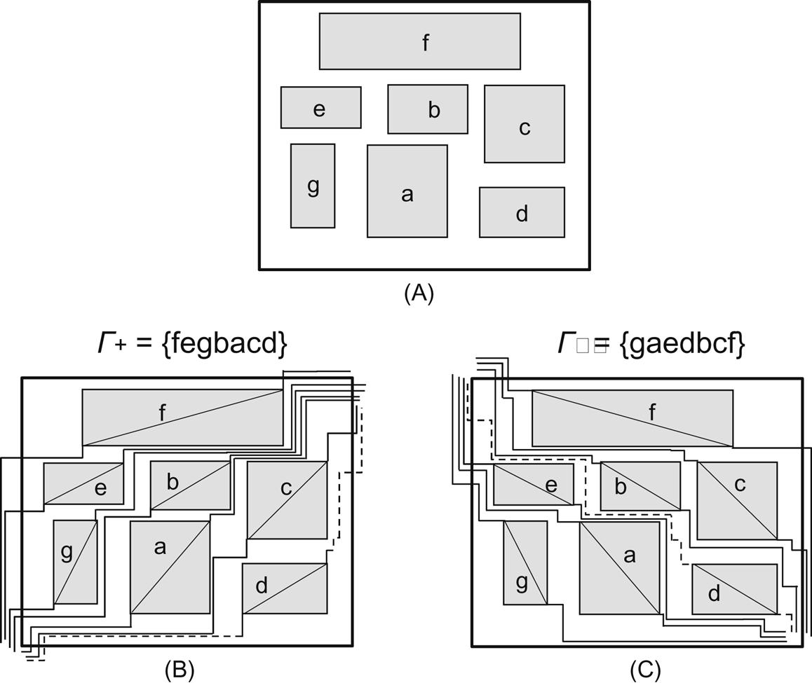
The salient feature of the SP technique is the formation of a pair of orderings of blocks that is floorplanned (or packed) within some area outline, as illustrated in Fig. 9.1. To generate a pair of sequences, several lines are formed according to three rules. The lines should not cross (1) the boundary of other modules other than the module for which the line is drawn, (2) previously drawn lines, and (3) the boundary of the outline. Two types of lines are drawn for every block, which are the “positive step line” and the “negative step line.” The positive step lines are formed for each block as follows. A line segment begins from the upper right corner of a block (say block b) and moves upwards and to the right in a stepwise manner towards the upper right corner of the circuit boundary, obeying the three rules. Additionally, another line segment begins from the lower left corner of the block and moves downwards and to the left towards the lower left corner of the circuit boundary. These two line segments with the diagonal line through b form the positive step line for block b. In a similar manner the negative step lines are formed, where the line segments for each block begin, respectively, from the upper left and lower right corners of the block. These segments are drawn by moving, respectively, up and left and down and right.

An example of these lines for the circuit blocks shown in Fig. 9.2A is illustrated in Figs. 9.2B and C, where the relevant lines for block d are depicted in this figure with dashed lines. The lines can be linearly ordered, leading to the two orderings for the blocks notated as Γ+ and Γ− corresponding, respectively, to the order of the positive and negative step lines. Based on Fig. 9.2, the SP is Γ+={fegbacd} and Γ−={gaedbcf}, which also provides useful information for ordering the blocks. Note that each block appears only once in each sequence and relates in four unique ways with the other blocks. For example, assuming two blocks s and s′, s can only appear after/before s′ in ![]() . To determine the relative position among the blocks, the four disjoint sets can be described where [338]
. To determine the relative position among the blocks, the four disjoint sets can be described where [338]
(9.2)
(9.3)
(9.4)
(9.5)
Based on these definitions, the following theorem has been proven [338]: assuming the SP (Γ+, Γ−) produced with the use of positive/negative step lines, the relative order of the blocks can be determined. Consequently, if ![]() , s is left of s′, if
, s is left of s′, if ![]() , s is right of s′, if
, s is right of s′, if ![]() , s is above s′, and if
, s is above s′, and if ![]() , s is below s′.
, s is below s′.
Based on this theorem, SP (Γ+, Γ−), and assuming that the circuit area is divided into an m×m grid, the optimal packing can be reached in O(m2) by utilizing the longest path algorithm [340]. In this process, horizontal and vertical constraint graphs are employed. Construction of these graphs is commonly used in physical design techniques [328]. More recent methods based on the SP representation have further reduced the complexity to produce floorplans in O(m log(m)) [340] and O(m log(log(m))) [341].
In addition to an efficient representation, producing high quality floorplans requires appropriate objective functions, where if the problem is packing driven, the objective is to minimize area, while connectivity driven functions emphasize minimizing wirelength. Many floorplan methods utilize cost functions that target both of these objectives and typically are of the form,
(9.6)
where the coefficients c1 and c2 indicate the importance of each of the two objectives. Area can be described, for instance, by (1+β)A. Irrespective of the formulation of the floorplanning problem, determining the area of the blocks within a floorplan is a straightforward process. Alternatively, at this early stage, wirelength cannot be accurately known. Among different models for calculating the wirelength, the half perimeter wirelength (HPWL) model is often utilized, where the efficiency of this metric for 2-D circuits has been evaluated by many techniques [342]. An example of HPWL is illustrated in Fig. 9.3.

The two objectives in (9.6) indicate a multiobjective optimization process even for the simplest floorplanning cost functions, requiring efficient solvers. Simulated annealing (SA) [343] is a popular solving technique that has been extensively applied to floorplanning and placement problems. The annealing process progresses towards an efficient floorplan by applying different block movements, such as swapping two blocks or rotating a block. Issues with this rather classic approach are that the wirelength is determined after each block movement and the solver only considers the size of the blocks, not the available whitespace. A more compact floorplan may be possible by moving a block to a different location within an outline of the floorplan (assuming this outline is fixed).
To address these issues of increasing computational time, approaches to handle incremental moves of the blocks have recently been explored which consider the whitespace. The notion of slack is borrowed from static timing analysis [344] and a spatial slack is assigned to a block sequence where the SP representation is employed. Similar to critical timing paths, a critical path for a floorplan is a sequence of blocks in the x- or y-direction adjacent and constrained with respect to each other to ensure that changing the site of a block causes neither an overlap or an increase in floorplan area. No whitespace in a specific path direction exists when a block is moved, similar to zero slack for the delay of a critical path. The slack analogy from timing analysis requires that all of the slacks (i.e., whitespace) of paths (i.e., sequences) of blocks must be determined for each direction, which is straightforward if the SP representation is followed. An example of slack computation for two different floorplans is depicted in Fig. 9.4. Subtracting the x coordinate of a block from the results when the blocks are packed, respectively, from left-to-right and from right-to-left, yields the x-slack of the block. Subtracting the y coordinate of this block from results when the blocks are packed, respectively, from bottom-to-top and top-to-bottom, yields the y-slack of the block.

The spatial slack information can lead to more efficient block moves to reduce the floorplan area. Block paths (or sequences) with zero slack are appropriate candidates for moves as these zero slack block paths determine the span of the floorplan along a physical direction. Moving a block from a path with high slack along a direction only mildly affects the length of the floorplan along this direction. Therefore, blocks within paths with zero slack along one direction but a large slack in the other direction are good candidates for single block moves. For example, a block with close to zero slack in both directions is a good candidate to be moved to a path with a large slack in both directions [332]. Application of these slack-based criteria for guiding block moves have led to improved results in producing valid floorplans, where a maximum 15% whitespace of the total block area is allowed and the outline is fixed. Considering whitespace in the floorplaning process becomes more important in 3-D circuits as significant area is consumed by the TSVs. Moreover, determining the wirelength for intertier connections where the TSVs are placed within whitespace regions can render the traditional HPWL metric a low accuracy estimate of the actual wirelength. These challenges require a different approach when floorplanning 3-D circuits.
9.2 Floorplanning Three-Dimensional ICs
An efficient floorplanning technique for 3-D circuits should adequately handle three important issues: representation of the third dimension, any related increase in the solution space, and the allocation (number and position) of the TSVs. These requirements affect specific aspects of the floorplanning process for 3-D circuits, such as the wirelength metric and the block representation. Techniques that investigate the first two issues considering the increased solution space are discussed in Section 9.2.1. The TSVs in these techniques are either assumed to be integrated within the 3-D circuit blocks (or cuboids) during floorplanning or to be placed anywhere across the entire tier as long as no overlap exists. In Section 9.2.2, floorplanning methods that bound the allocation of TSVs within a 3-D circuit are reviewed. These techniques emphasize the effect of inserting TSVs on several design objectives. These results demonstrate that a planning step for TSV allocation is indispensable when floorplanning 3-D circuits.
9.2.1 Floorplanning Three-Dimensional Circuits Without Through Silicon Via Planning
Certain algorithms incorporate the 3-D nature of the circuits, such as a 3-D transition closure graph (TCG) [345], sequence triple [346], and a 3-D slicing tree [347], where the circuit blocks are notated by a set of 3-D modules that determine the volume of a 3-D system. Utilizing these notations for the circuit blocks, an upper bound for 3-D slicing floorplans is determined [348]. In 3-D slicing floorplans, a tier successively bisects the volume of a 3-D system. The upper bound for 2- and 3-D slicing floorplans is illustrated in Fig. 9.5. The coefficient r shown in Fig. 9.5 is the shape flexibility ratio and denotes the maximum ratio of the dimensions of the modules (i.e., max(width/height, depth/height, width/depth)). This ratio is assumed to be greater than two. The use of this ratio implies that all modules are assumed to be “soft blocks.” Moreover, as observed in Fig. 9.5, Vtotal is the sum of the volume of the blocks that comprise the target system, and Vmax denotes the maximum volume among the blocks. In general, 3-D floorplans result in larger unused space as compared to 2-D slicing floorplans primarily due to the highly uneven volume of the 3-D modules. For high flexibility ratios, however, this gap is considerably reduced and, in certain cases, the upper bound for 3-D floorplans is smaller than in 2-D floorplans.

Although a high flexibility ratio offers more compact floorplans with less unused area, this assumption may not be practical as changing the length of a circuit block along the z-direction (i.e., changing the number of tiers spanned by a block) can greatly affect the number of intertier connections required by this block. This number can affect, in turn, the number of blocks violating the assumption that the volume of the block remains constant for all values of r. Furthermore, treating blocks as soft (variable r) is not an option for IP blocks developed for 2-D systems. These legacy circuits can often be hard macros where the size of these blocks is unlikely or not permitted to change if, for example, some circuits originate from a third party source. This situation can lead to less compact floorplans with significant whitespace. Although this restriction results in area overhead, the whitespace can, alternatively, be used to insert TSVs for signaling, power and ground distribution, and thermal management, thereby avoiding additional area overhead.
Another computational issue relates to the notation of the dimensions of the blocks as continuous variables. The use of continuous variables is convenient as analytic methods can be used to accurately determine bounds or optimally solve similar problems. The third dimension, however, should be treated as a discrete variable, which can produce suboptimal solutions if continuous analytic methods are applied, since the blocks must be placed into a small number of physical tiers. Consequently, 3-D systems are more efficiently described as an array of two-dimensional planes where the circuit blocks are treated as rectangles rather than cuboids placed on any of the planes constituting the 3-D circuit [349–351]. This approach reduces complexity; despite the number of blocks increasing with the number of stacked tiers. The combinations rise drastically, exacerbating the solution space for floorplanning a 3-D system. This second challenge for 3-D floorplanning, which is to effectively explore the solution space within reasonable time, has led to multistep approaches that often are more efficient for floorplanning 3-D circuits than a single step approach.
In 3-D circuits, a multistep floorplanning technique commences by partitioning the blocks among the tiers of a stack [352]. An illustration of single and multistep approaches is shown in Fig. 9.6. In single step floorplanning algorithms, the floorplanning process proceeds by assigning the blocks to the tiers of a stack followed by simultaneous intratier and intertier block swapping, as depicted in Fig. 9.6. Alternatively, a multistep approach does not allow intertier moves after the partitioning step. The reason for this constraint is that intertier moves among blocks result in a formidable increase in the solution space, greatly affecting the computational time of a single step floorplanning algorithm. Indeed, assuming N blocks witihin a 3-D system consisting of n tiers, a flat floorplanning approach increases the number of candidate solutions by Nn−1/(n−1)! times as compared to a 2-D circuit consisting of the same number of blocks. The solution space for floorplanning 2-D circuits based on the TCG technique [335], and 3-D circuits with a single and multistep approach are listed in Table 9.1. Consequently, a multiphase approach can be used to significantly reduce the number of candidate solutions.

Table 9.1
Solution Space for 2-D and 3-D IC Floorplanning [352]
| Characteristic | 2-D IC | n-Tier 3-D IC | |
| TCG | TCG 2-D Array | Multistep | |
| Solution space | |||
| Ratio | 1 | ||

The partitioning scheme adopted in the multistep approach plays a crucial role in determining the compactness of a particular floorplan, as intertier moves are not allowed when floorplanning the tiers. Different partitions correspond to different subsets of the solution space which may exclude the optimal solution(s). The objective function for partitioning should therefore be carefully selected. Due to the silicon area of the TSVs, reducing the number of intertier connections is a reasonable objective. This objective typically minimizes the number of TSVs across the entire stack. Thus min-cut algorithms, such as the hMETIS algorithm [353], can be employed to produce 3-D partitions. However, other alternatives exist where the number of TSVs is not an objective for partitioning but rather a constraint. The partitioning can, for instance, be based on minimizing the estimated total wirelength of the system [352]. For example, a partitioning problem based on minimizing the estimated total wirelength can be described as
(9.7)
(9.8)
where ELnet is the estimated interconnect length connecting two blocks of a 3-D circuit, which can contain both horizontal and vertical interconnect segments. This estimate is not based on the traditional HPWL metric but is probabilistically determined [352]. The total number of intertier vias is denoted by TNvia, and the maximum number of allowed intertier vias within a 3-D system is notated by TVmax.
The issue is therefore which target objective will produce a more compact floorplan with shorter wirelength. If the cut size is proportionally related to the total wirelength, minimizing the cut size decreases not only the area of the TSVs but also the wirelength. Alternatively, if the dependence of wirelength on the number of TSVs is loose, from (9.7) and (9.8), where the TSV count approaches the upper bound may be a better choice, as more intertier connections will reduce long horizontal wires.
A 3-D floorplanner for two tiers based on [350] has been applied to the benchmark circuits included in the Microelectronic Center of North Carolina/Gigascale Research Center (MCNC/GSRC) benchmark suite [355] to better evaluate this tradeoff. The partition is based on [356] where a fixed cut size is utilized. The cut size is neither the minimum nor the maximum, as these extrema cut sizes limit the flexibility of the partition algorithm [354]. Rather, a fixed cut size lying between these bounds is employed. In addition, a 5% imbalance in area between the two tiers is allowed, and the whitespace is set to 20% of the total area of the blocks. Results of this evaluation indicate that partitioning is not important for circuits where the interconnects among blocks exhibit a narrow wirelength distribution (e.g., the n100, n200, and n300 benchmarks). Alternatively, circuits that include interconnects with a wide distribution of lengths are affected more by the partitioning step (e.g., ami33 and ami49). In addition, results characterizing the relationship between the total wirelength and the number of vertical interconnects across the tiers of the stack demonstrate that the total interconnect length does not strongly depend on the cut size if the circuit consists of a small number of highly unevenly sized blocks. This behavior can be attributed to the significant computational effort required to optimize the area of the floorplan rather than the interconnect length. Alternatively, in circuits composed of uniformly sized blocks, an inverse relationship between the number of vertical vias and the interconnect length is demonstrated. These results are useful indicators when floorplanning a multitier circuit, although the fixed cut size has only been applied to two tier circuits. It is unclear whether the same behavior occurs in stacks with more than two physical tiers.
The partitions are an input to another phase of the multistep process where the floorplan of each tier of a 3-D circuit is generated. Note that the floorplan of each of the tiers is simultaneously produced. In [352], the circuit blocks are represented in three dimensions by the corner block list method [337], while in [354], the SP [338] is used to represent the floorplans. In both of these techniques, SA is employed to produce the floorplans. For single step approaches, where partitions are not available, the starting point for the SA engine is generated by randomly assigning the blocks to the tiers of the system to balance the area of the individual tiers. The SA process progresses by swapping blocks between two tiers (for single step approaches) or changing the location of the blocks within one tier. A candidate solution is therefore perturbed by selecting a tier within the 3-D stack and applying one of the moves described in [337]. The expected wirelength and number of vertical vias are reevaluated after each modification of the partition (which can be a computationally expensive step, as mentioned in the previous section), where the algorithm progresses until a floorplan is obtained at the target low temperature of the SA algorithm.
Application of the technique in [352] (with bounded but not fixed TSVs) to the MCNC and GSRC benchmark suites [355] with a comparison to the TCG-based 2-D array and the combined bucket and 2-D array techniques (CBA) [351] is provided in Table 9.2. A small reduction, on the order of 3%, in the number of vertical vias and a significant reduction of approximately 14% in wirelength is exhibited, while the total area increases by almost 4% for certain benchmark circuits.
Table 9.2
Multistep Floorplanning Results [352]
| Benchmark | TCG-Based 2-D Array | CBA | Multistep Floorplanning | ||||||
| Area | Wirelength | Vias | Area | Wirelength | Vias | Area | Wirelength | Vias | |
| ami33 | 3.52E+05 | 23,139 | 106 | 3.44E+05 | 23,475 | 111 | 4.16E+05 | 21,580 | 108 |
| ami49 | 1.49E+07 | 453,083 | 191 | 1.27E+07 | 465,053 | 203 | 1.42E+07 | 420,636 | 198 |
| n100 | 53,295 | 97,066 | 704 | 51,736 | 90,143 | 752 | 54,648 | 74,176 | 733 |
| n200 | 51,714 | 198,885 | 1487 | 50,055 | 175,866 | 1361 | 55,944 | 142,196 | 1358 |
| n300 | 74,712 | 232,074 | 1613 | 75,294 | 230,175 | 1568 | 79,278 | 213,538 | 1534 |
| Avg. | 1.00 | 1.17 | 1.03 | 0.96 | 1.14 | 1.02 | 1.00 | 1.00 | 1.00 |

Although the techniques discussed in this section utilize a different metric for wirelength, both the HPWL and the probabilistic wirelength estimate in [352] neglect the increase in wirelength due to the placement of the TSVs and the wires. Including the effect of the TSVs in the floorplanning process requires different metrics and approaches, as discussed in the following subsection.
9.2.2 Floorplanning Techniques for Three-Dimensional ICs With Through Silicon Via Planning
The complexity of 3-D integration requires different wirelength metrics and advanced cost functions that include several objectives beyond area and wirelength (A/W) to produce efficient floorplans for 3-D circuits. These objectives can consider, for example, the communication throughput among the circuit blocks and/or the number of intertier vias. The effect of utilizing more accurate metrics than the traditional model of the half perimeter of the bounding box of the nets to estimate the length of the intertier nets is discussed in Section 9.2.2.1. Approaches to integrate TSV planning with the floorplanning process are presented in Section 9.2.2.2, while techniques treating the TSV planning as a post-floorplanning step are reviewed in Section 9.2.2.3. Practical issues in inserting TSVs within whitespace also used by other resources are considered in Section 9.2.2.4, where some nonconventional approaches to floorplanning are briefly mentioned.
9.2.2.1 Enhanced wirelength metrics for intertier interconnects
In addition to the cut size or, equivalently, the number of connections between tiers, the processing technique to bond the tiers of a 3-D circuit also affects the partition step in a multistep floorplanning methodology. The various bonding mechanisms employed in a 3-D system contribute in different ways to the final floorplan as these bonding styles support different densities of vertical wires (i.e., TSVs) with dissimilar electrical characteristics.
For example, front-to-front bonding produces a large number of short intertier vias, improving the performance of those modules with a high switching activity. Furthermore, a block with a large area can be divided into two smaller blocks assigned to adjacent tiers and employ front-to-front bonding to minimize the effect of the physical separation on the performance and power consumption. Alternatively, intertier vias utilized in front-to-back bonding can adversely affect the performance of a 3-D system if not used with caution due to the overhead in active area of these interconnections. In addition, TSVs require a different approach for determining the wirelength of a 3-D system. This situation occurs if a TSV is placed outside the bounding box of the net containing the TSV.
To better explain this situation, an example is depicted in Fig. 9.7 where blocks within a three-tier system are illustrated. A net connects the pins p1,1, p1,2, and p1,3, (depicted with solid squares), respectively, of blocks b1, b2, and b3, employing TSVs v1,12 and v1,23 (depicted with solid circles). In Fig. 9.7A, all of the pins of this net across the stack are projected onto tier 1. The projected pins from tiers 2 and 3 are shown with empty squares. If the classic HPWL is employed to determine the length of this net, this length is LHPWL=w+h, as determined by the rectangle drawn with a dashed-dotted line. HPWL, however, does not include the segments of the nets to the TSVs, thereby, for this specific example, underestimating the length. To address this issue, the bounding box of the net assumed in Fig. 9.7A is extended to include the TSV locations [357]. The new bounding box plotted in Fig. 9.7B with the dotted line results in a new length equal to LHPWL-TSV=w′+h′ which is greater than LHPWL. To determine LHPWL-TSV, all of the pins and TSVs are projected onto a single tier, tier 3 in this specific example. If the location of the TSVs is contained within the dashed-dotted bounding box of the net shown in Fig. 9.7A, LHPWL=LHPWL-TSV. This situation is however unlikely to occur, in particular if floorplanning is at the block level, where longer interconnects typically occur. Although including the TSV locations when determining the length of the nets produces a better estimate as compared to HPWL, greater accuracy is achieved if the individual segments of the net in each tier are considered. In this approach, the bounding box—typically between a pin and a TSV—is determined for each tier. Consequently, the total length of the net is LHPWL-NET-SEG=(w1+h1)+(w2+h2)+(w3+h3), where the length of each segment is assumed to be the HPWL of the bounding box of this segment depicted by the dashed lines. Note that, for this example, LHPWL-TSV=(w2+h2) < LHPWL-NET-SEG.

All of these metrics have been used to estimate wirelength during floorplanning of 3-D circuits. Intuitively, these metrics produce similar results if the floorplanning process generates whitespace close to the pins connected to the intertier wires. The TSVs in this case can be placed within the bounding box determined solely by the pins projected onto a single tier. Furthermore, the whitespace does not include a single TSV but rather several TSVs; therefore, the notion of a TSV island is introduced [357]. Each TSV island is associated with a capacity, which can be adapted to accommodate a greater number of TSVs without incurring a considerable length overhead for certain nets. In this case, the center of the island determines the vertex of the bounding box rather than a single TSV. Consequently, the TSVs can have a nonnegligible effect on the length of the intertier nets, which should be considered when floorplanning a 3-D circuit, as discussed in the following subsection.
9.2.2.2 Simultaneous floorplanning and through silicon via planning
These advanced wirelength metrics are useful to perform accurate TSV planning for 3-D floorplans while producing short wirelengths to achieve a target stack. The steps of a general floorplanning methodology including TSV planning are illustrated in Fig. 9.8, where an SA engine and SP representation produce candidate floorplans. The input of the process includes: (i) a set of blocks with fixed dimensions (fixed aspect ratio), (ii) a netlist indicating connections among the blocks, (iii) the dimensions and number of tiers, and (iv) the physical parameters of the TSVs for the target technology. The objective of the technique is to determine: (1) the coordinates of each block including the tier number, (2) the coordinates and size of the TSV islands, and (3) for every TSV within each tier, the TSV island in which a TSV is allocated. Related constraints are: (1) no block coordinate can exceed the dimensions of the tier (assuming a fixed outline), (2) no block overlap is allowed, and (3) the total area of the TSVs assigned to a TSV island does not exceed the area of this island.

The process, shown in Fig. 9.8, proceeds as follows. A floorplan is randomly produced and successive perturbations are performed to generate low cost floorplans, where the cost function is [357]
(9.9)
The last term penalizes any change in the aspect ratio of the floorplan. Note that this expression does not differ considerably from (9.6) used in 2-D circuits. The area now includes, however, the area of the TSVs, and the wirelength metric LHPWL-TSV is considered rather than LHPWL.
The perturbations of a solution are based on the notion of slacks, as described in Section 9.1, where the horizontal and vertical slack for each block is determined. The perturbations include: (1) intertier swapping of a block or a pair of randomly chosen blocks, and (2) moves of blocks between tiers to balance the area among the tiers. The blocks in congested tiers are given a higher probability to be relocated. (3) The spatial slack information is used to perform a block move, where blocks of opposite slack are placed close to each other.
Based on the floorplan produced after applying these perturbations, the cost function shown in (9.9) determines whether the most recent iteration of the floorplan is accepted. If accepted, the TSV planning step commences. This step progresses by assigning in a greedy way a TSV into a TSV island. As the annealing temperature cools, a more detailed TSV assignment follows. During the greedy assignment process for each intertier net, the bounding box (see Fig. 9.7B) can contain several whitespaces, which are used as TSV islands. If several of these TSV islands for a tier exist, a TSV is placed within any of these islands with equal probability, yielding no increase in wirelength. This practice may, however, lead to some islands with more TSVs than is physically possible. The area of these islands is expanded to fit the excessive number of TSVs. The resulting overlap between the TSV islands and surrounding blocks is resolved during the finer assignment step. The reason for allowing the overlap is that no increase in wirelength occurs if as many TSVs as possible are kept within those islands contained within the bounding box of a net. The increase in area, however, should not outweigh the savings in wirelength.
Consequently, the stage of TSV refinement uses two pieces of information to decide how best to allocate the TSVs into an island. The TSVs are sorted according to the total area of the candidate TSV island(s) where a TSV is placed. Candidate TSV islands are contained within the bounding box of a net, as illustrated in Fig. 9.9, where some noncandidate TSV islands for a specific net are also shown. The smaller the area of the island, the higher the priority for a TSV. As this island can be more quickly filled, the TSV may be placed within another TSV island, potentially beyond the bounding box. To avoid these expensive placements, if the candidate island for a TSV has been filled, allocation of this TSV is deferred to a later step in the process.

At the end of this stage, some TSVs may not have been assigned to any of the candidate TSV islands. Two options can be followed, either expanding the area of a candidate TSV island or assigning one TSV to a noncandidate TSV island (i.e., a TSV island not inscribed within the bounding box of the net containing the TSV). In both cases, the wirelength relates to the nets crossing the expanded TSV island or the additional wire segment needed to reach the noncandidate island. A linear cost function to consider the increase in wirelength caused by either option is used in [357]. The option with the lower cost is selected, leading to an iteration to produce a floorplan if an expansion is chosen. If the additional wire connecting a pin to a TSV island outside the bounding box of the net is longer than the increase in wirelength due to the expansion of a candidate TSV island, the latter option is chosen. The computational cost required to generate a new floorplan should however be considered. In addition, this choice implicitly favors wirelength reduction over area minimization, which may increase the difficulty of the SA algorithm to produce a high quality floorplan, particularly if greater emphasis is placed on the area or aspect ratio term in (9.9).
A limitation of this flow is that the TSVs are treated individually, potentially leading to suboptimal results. To improve the quality of the solution, another stage of TSV reassignment, notated as stage II in Fig. 9.8, is added to the flow, where the main task is to reassign TSVs among the TSV islands. The area and number are fixed to further reduce the wirelength. The task is formulated as a minimum cost maximum flow problem which can be optimally solved in polynomial time [358].
The technique described in [357] has been applied to benchmark circuits used in physical design problems, such as the ami, n100, n200, and n300 benchmark circuits, and is compared with a TSV unaware floorplanning method where the length of the nets is LHPWL. In addition, the location of the TSVs is considered after a floorplan is generated and not during the floorplanning process. These results, listed in Table 9.3, demonstrate improved wirelength while satisfying a fixed outline constraint with an increase in computational time (attributed to the TSV planning steps within the floorplanning process).
Table 9.3
Flooplan With and Without TSV Planning [357]
| # of Tiers | Circuit | TSV Aware | TSV Unaware | ||||||
| Success Rate | Avg WL | TSVs | Time (s) | Success Rate | Avg WL | TSVs | Time (s) | ||
| 3 | n100 | 100% | 160,825 | 833.2 | 1195.91 | 80% | 157,480 | 888.8 | 22.68 |
| 3 | n200 | 100% | 310,924 | 1509.1 | 7720.45 | 0% | 339,768 | 1689.5 | 87.38 |
| 3 | n300 | 100% | 424,585 | 1899.7 | 21155.10 | 0% | 440,954 | 2019.3 | 159.02 |
| 4 | n100 | 100% | 148,748 | 1171.4 | 1306.39 | 90% | 165,940 | 1290.5 | 23.38 |
| 4 | n200 | 100% | 291,091 | 2179.0 | 8237.10 | 0% | 367,602 | 2431.5 | 94.45 |
| 4 | n300 | 100% | 391,694 | 2730.6 | 21450.50 | 10% | 448,905 | 2865.0 | 234.12 |

9.2.2.3 Through silicon via planning as a post-floorplanning step
A different path to plan and insert TSVs can also be followed where the size of a TSV island is insufficient to fit the assigned TSVs. In the previous subsection, this situation is handled by increasing the size of the whitespace or allocating a TSV to an island located farther away. The increase in size of the TSV islands is considered in the next floorplanning iteration. Alternatively, this increase can be achieved by avoiding a floorplanning iteration if area is borrowed from other whitespace regions. Although this borrowing shifts blocks, this process can be performed by shifting only specific blocks in the vicinity of this island rather than floorplanning the entire circuit. In this way, any fixed outline constraint is easily satisfied. To perform these block shifts, however, information describing the slack of all of the blocks of the circuit should be available. The technique, discussed in [339], utilizes this information to treat TSV planning as a post-floorplanning step.
A fixed outline 3-D floorplan with no overlaps among blocks is the primary input of this technique, where the coordinates of each block are xb and yb, and nb is the physical tier in which the block is placed. Other inputs include the number of TSV islands, where each island has a specific capacity and dimensions (hTSV_island, wTSV_island), and a netlist describing the connections among the blocks. As LHPWL-NET-SEG provides an improved estimate of the wirelength, this metric is employed to determine the total wiring of the circuit. Although LHPWL-NET-SEG is a better estimate, LHPWL-TSV is faster to determine and is, therefore, used if the granularity of the floorplanning/placement is at the gate level rather than at the block level. Employing TSV islands at the gate level results in unacceptably long wires since the TSV should be placed adjacent to the connecting cell. Additionally, at the block level, providing capacity for each TSV island is not a straightforward task and can affect the quality of the overall floorplan. The decision for the TSV island capacity can be based either on user experience or on a probabilistic allocation of capacities similar to the assignment process of inserting TSVs into islands [357]; however, no evidence exists as to whether these input parameters affect the resulting floorplan.
The approach of [339] clusters intertier connections to TSV islands, and assigns each of these clusters to a whitespace. The clustering step employs the notion of a “virtual die,” which is depicted in Fig. 9.10. The bounding box of the nets is projected onto the virtual die, and the intersection of several boxes forms a cluster with the respective nets. The capacity of the available TSV islands determines the number of clustered nets or, alternatively, the number of bounding boxes projected onto the virtual die of a TSV island.

An intersection graph is defined to determine the intersection of the overlapping bounding boxes, where the vertices correspond to bounding boxes while overlaps among blocks are expressed by edges. To determine the common region, a number of cliques are determined where the size of each clique satisfies the capacity of the target TSV islands. This step is NP-complete [359].
With the area of the whitespace across each tier known, the TSV islands are assigned to these areas where some whitespace may not be used for a TSV island or can be shared by more than one TSV island. Additionally, a net can include more than one TSV contained within several TSV islands. As previously discussed, the TSV assignment process can be achieved probabilistically or with some dynamic metric which considers the decreasing available whitespace as the TSV assignment process proceeds. An example of this metric is
(9.10)
which considers the available whitespace of a cluster as compared to the number of assigned nets within a cluster. Although clusters with high scores are prioritized to reduce the number of unassigned nets, by the end of the process, nets can exist which have not been assigned to a cluster. Failing to insert a TSV island means that greater whitespace is necessary, which can be achieved through two different schemes [339]. Additional whitespace can be made available by adding channels of whitespace between blocks to accommodate the TSVs as well as buffers and local logic. This straightforward method increases the overall area of the floorplan. Alternatively, the available whitespace can be redistributed to provide the required area within each tier.
Greater whitespace can be achieved by shifting the blocks, which eliminates unnecessary use of whitespace (for example, outside the common region of the projected bounding boxes of the nets, see Fig. 9.10B), thereby increasing the available area for other islands. Block shifting is performed in two ways, producing successful TSV assignments, where (1) the blocks are shifted at the beginning of the TSV planning process, and (2) the blocks are successively shifted during the TSV island insertion step. To determine the available shifting opportunities, the notion of spatial slack is used as previously discussed. The use of slack allows the fragmented and otherwise unsuitable whitespace to be consolidated among blocks in the x and y directions without increasing the area, leading to a more compact floorplan.
Experiments on standard benchmark circuits have shown that initial shifting performs better than iterative shifting in terms of the total wirelength, although the latter shifting is performed dynamically. A rationale for this preference is that during initial shifting none of the TSV islands has been assigned and full slacks can be exploited, albeit only once. During iterative shifting, the gradual insertion of TSV islands quickly dissipates the available slack, decreasing the likelihood of redistributing whitespace to provide additional space for the remaining TSV islands. Alternatively, channel insertion is achieved by first proportionally inflating the dimensions of the blocks and then contracting the blocks to the original dimensions after a floorplan is produced. The increased whitespace can, in this case, efficiently fit the TSV islands; yet an approximately 10% increase in the total area of the circuit is incurred. Moreover, the total wirelength is shorter due to iterative block shifting but longer than from the initial block shifting.
Note that all of the techniques discussed in this section assign a group of TSVs to some empty space but do not assign individual TSVs within this space (this problem is considered in Chapter 10, Timing Optimization for Two-Terminal Interconnects, and Chapter 11, Timing Optimization for Multiterminal Interconnects, where early timing driven techniques for TSV placement are presented). The coordinates at the center of the TSV islands are used to provide wirelength estimates, resulting in pessimistic estimates and potentially producing a suboptimal placement of TSVs.
Although enhanced wirelength metrics and TSV islands improve the quality of the floorplan, inserting TSV islands can still fail despite increasing the floorplan. This limitation can be alleviated if an alternative approach is followed, where the pins of the block, the bounding box of the nets, are moved along the boundary of the blocks to provide greater flexibility in allocating TSVs within each tier. Alternatively, pin assignment for each block is another degree of freedom to reduce wirelength. Moving pins leads to disparate bounding boxes that contain more or larger capacity TSV islands. This approach is also applied as a post-floorplanning technique to minimize wirelength, where the solution to the optimization problem places both the TSVs of the intertier net as well as the pins of each block [360]. The technique adapts the problem to ensure that a minimum cost maximum flow algorithm is applied. A solver with a time complexity of O(|V|2|E| log(C|V|)), where V and E denote the vertices and edges of the related graph constructed for the target problem and C is the maximum cost of the arcs within the graph [358]. The technique optimally solves the case where a block is connected to several blocks through single and/or multiple fan-out nets. The algorithm determines the position of the pins and TSVs to minimize the wirelength of the nets. Alternatively, for the algorithm to be optimally solved, the multipin nets can be decomposed into several two-pin nets. This task requires the use of additional source terminals. The technique proceeds by replicating pins for the specific net at the source block. Once the minimum cost maximum flow algorithm terminates, the replicated pins are mapped back into the original pin, which can produce a nonoptimal floorplan. Furthermore, in practical systems, blocks are connected in many different ways. Many blocks behave both as a source and destination for different nets. A straightforward procedure to cope with this issue is to successively apply the single block source—multiple block destinations problem to all blocks within a system where the blocks are randomly chosen. The optimality of this process is however not guaranteed. In addition, HPWL is used as the wirelength metric which performs poorly in 3-D circuits. Consequently, although the technique reduces the wirelength by simultaneously manipulating pins and TSVs, additional space for decreasing the wirelength is possible through enhanced TSV planning.
9.2.2.4 Practical considerations for floorplanning with through silicon via planning
The use of whitespace has to date been limited to the important resource of TSVs. Unoccupied regions in 2-D circuits have, however, traditionally been used for repeaters and decoupling capacitors, particularly in the case where the circuit is comprised of hard macros. Consequently, in 3-D circuits, repeaters and TSVs share the same whitespace. Furthermore, TSV planning techniques which only focus on assigning TSVs to the available whitespace do not consider the effect that this assignment can have on the non-optimal placement of repeaters for intertier nets. Since these nets tend to be the longest interconnect in a multitier system, this situation can degrade system performance. To address this problem, repeaters and TSVs should be simultaneously placed to better utilize the available whitespace.
Employing the concept of (independent) feasible regions [361,362], the largest polygon should be placed to satisfy local timing constraints. Simultaneous buffer and TSV insertion improve timing closure for these intertier nets [363]. If this feasible region overlaps the whitespace, the intersection between these two areas represents a valid location for these buffers. The intertier nets, however, require a different treatment as the feasible regions should be determined for each tier before placing buffers in those tiers. Consequently, a two-step process is followed where the feasible regions for each tier spanned by the target net are determined, while simultaneously, TSVs are inserted within these regions.
The second step is allocating buffers and TSVs to each tier. To better describe this process, an example of an intertier net is illustrated in Fig. 9.11, where the pins of the net are in tiers one and three, and k buffers are assumed to be needed. The feasible region for the second tier is shown in Fig. 9.11. The feasible regions within each tier are similarly determined. Since all of these regions are candidates for buffers driving the same net, a buffer connection graph is employed to link these regions together. An example of this graph is shown in Fig. 9.11B for the net depicted in Fig. 9.11A. The rows in this graph represent the tiers spanned by the net, and the columns represent the number of inserted buffers (k=3 in this example). Thus, the vertex indicated by (rowi, columnj) means that the jth buffer can be placed in tier i. A vertex does not exist in (row1, column3), which means that the third buffer cannot be placed in the feasible region of that tier. The edges of the graph indicate whether a TSV can be placed within the feasible regions of the tiers connected by this TSV. The projections of the two feasible regions from two adjacent tiers intersect, resulting in a nonempty (available) area for placing a TSV. In this example, edge e means that a TSV can be placed between tiers 1 and 2 connecting the buffers in the corresponding feasible regions while satisfying existing timing constraints. The edges among vertices in the same row simply indicate that routes between buffers of the same tier are possible.

With this graph describing the connections of the buffers and TSVs, the location of these items need to be determined, preferably in a form of a path connecting the pins of a net. An example path is illustrated in Fig. 9.11C, where other paths are also shown. The choice of the path is supplemented by other objectives in addition to timing and wirelength, such as congestion, by adapting the weight of the edges. The path with the lowest cost is chosen for each net.
The complexity of this technique is O(mn2Mbuf), where m is the number of nets, n is the number of tiers, and Mbuf is the greatest number of buffers required for a net among the P interconnections. Considering that the complexity of the method is linear with the number of nets and that the number of buffers and tiers are low, buffer and TSV planning can be integrated with floorplanning. Similar to other techniques, whitespace redistribution offers a means to further improve the efficiency of this technique. A heuristic is employed [357] based on the constraint graphs along the two physical directions x and y, which provide the spatial slack of each block as in [339]. This heuristic, however, does not shift any of the blocks during the TSV allocation process but rather assigns a TSV to a region, expanding the area of the whitespace during subsequent floorplanning iterations.
The blocks can be shifted only after all of the TSVs and buffers have been allocated. Breadth first traversals along the horizontal and vertical directions within each tier are applied to expand the feasible regions based on spatial slack information. If the greatest possible shift of blocks does not enable the assignment of all TSVs, the floorplan is perturbed, initiating a new iteration. SA is utilized for floorplanning but the typical linear cost function is extended and annealing proceeds in three different stages, where a different cost function is utilized to emphasize a different objective. Thus, the first stage emphasizes area as the modules are initially far apart (high temperatures of the annealing process). As the compactness of the floorplan increases, timing is also added to the cost function, as described by
(9.11)
where the timing violations are included in the cost function. If during this phase, the temperature slowly decreases, another term is added to the cost function (which constitutes the third stage) which satisfies the timing of those intertier wires with unassigned buffers and TSVs. Note that the same perturbations as in [352] are applied, where intertier moves for blocks are disallowed.
The performance of the simultaneous treatment of buffers and TSVs has been explored on two MCNC and other synthetic benchmark circuits. Some of these results are reported in Table 9.4, where these benchmark circuits are floorplanned in a single tier without (F2D/NWR) and with whitespace redistribution (F2D/WR) using the SA approach from [356]. These results are compared to the 3-D floorplanner without (F3D/NWR) and with (F3D/WR) whitespace redistribution where a four tier system is assumed. A comparison of the A/W for these scenarios shows that F3D/WR performs best where redistributing the whitespace slightly improves the floorplans (4.8% and 2.4% for, respectively, wirelength and area). The disadvantage of whitespace redistribution is, however, a higher number of buffers and TSVs, as listed in, respectively, columns 9 and 10 to improve the timing of the circuit. Therefore, additional nets can satisfy the timing requirements, as listed in columns 11 and 12 of Table 9.4.
Table 9.4
Comparison of 2-D and 3-D Floorplans With and Without Whitespace Redistribution for Simultaneous Buffer and TSV Planning [363]
| Circuit | Area (mm2) | Wirelength (mm) | B/#B | Net Timing Met | Net Timing Failed | Area (mm2) | Wirelength (mm) | TSV/#TSV | B/#B | Net Timing Met | Net Timing Failed |
| F2D/NWR | F3D/NWR | ||||||||||
| ami33 | 1359.16 | 5922.63 | 52.30% | 241 | 70 | 1317.72 | 3937.08 | 76.29% | 58.48% | 279 | 84 |
| ami49 | 1373.10 | 8921.08 | 79.73% | 353 | 156 | 1095.68 | 5781.72 | 79.37% | 68.16% | 381 | 164 |
| F2D/WR | F3D/WR | ||||||||||
| ami33 | 1251.02 | 5745.40 | 33.05% | 213 | 43 | 1350.52 | 3519.18 | 92.17% | 86.04% | 317 | 46 |
| ami49 | 1067.57 | 9663.90 | 68.35% | 330 | 188 | 1068.64 | 5185.88 | 95.85% | 94.33% | 432 | 113 |

9.2.2.5 Microarchitecture aware three-dimensional floorpanning
Before closing this discussion on the various aspects of 3-D floorplanning, it is worth noting that disruptive approaches for floorplanning 3-D circuits have been developed, where the length of the nets is weighted differently. Thus, a communication-based objective can utilize information from the microarchitectural level, resulting in floorplans with a higher number of instructions per cycle (IPC) [364]. In a 3-D system, blocks that communicate frequently can be assigned to adjacent tiers, decreasing the interconnect length of the interblock connections. The communication throughput is also increased while reducing the power consumed by the system. Alternatively, blocks with high switching activities should not overlap in the vertical direction to ensure that the temperature profile of the system remains within specified limits. Consequently, the communication throughput is carefully balanced with operating temperature.
A multi-objective floorplanning approach targeting microprocessor architectures is illustrated in Fig. 9.12, where a variety of tools characterize different parameters of the functional blocks within a processor. The CACTI [365] and GENESYS [366] tools provide an estimate of the speed, power, and area of the processor. The SimpleScalar simulator [367] combined with the Watch [368] framework records the information exchanged across the system to predict the power consumption of each benchmark circuit. A hierarchical approach is utilized where the SA engine is replaced by a slicing algorithm based on recursive bipartitioning [369]. This algorithm distributes the functional blocks of the processor onto the tiers of the 3-D stack to decrease computational time.

The additional objectives include area and wirelength (A/W), area and performance (A/P), area and temperature (A/T), and area, performance, and temperature (A/P/T). Based on evaluating MCNC/GSRC benchmark circuits, A/W achieves the minimum area as compared to the other objectives, decreasing by almost 40% the interconnect length as compared to a 2-D floorplan of the same microarchitecture. A/P increases the IPC by 18% over A/W, while simultaneously increasing the temperature by 19%. The more complex objective A/P/T generates a temperature close to A/W, while the IPC increases by 14%. In general, the performance generated by the A/P/T objectives is bounded by the performance provided by the A/T and A/P objectives. In addition, A/P/T achieves higher performance as compared to A/W with a similar temperature [364].
9.3 Placement Techniques
Placement algorithms traditionally target minimizing the overall area of a circuit and the interconnect length among the cells, while reserving space for routing the interconnect. A brief discussion of the different approaches used for placing 2-D circuits is offered in this section, where specific techniques are described in greater detail to provide the necessary background for applying 2-D placement techniques to 3-D circuits.
As with floorplanning, SA is also applied to placement problems [370], but the large number of cells in the placement step as compared to the fewer number of blocks during floorplanning can result in excessive computational time [371]. Other placement methods are based on partitioning, where the netlist and area of a circuit are successively partitioned, minimizing the number of connections between juxtaposed partitions during each partitioning step. Some placers rely on partitioning methods including, for example, Capo [372] and Fengshui [373].
In addition to stochastic and min-cut placement methods, another category includes analytic-based placers where an appropriate cost function is optimized for a specific single objective or multiple objectives through a combination of diverse optimization methods. The cost functions can be, in general, nonlinear and quadratic (as compared to typical linear cost functions assumed in SA-based techniques). Examples of nonlinear placers include NTUplace [374] and mPL [375].
In quadratic placement, the wirelength is described as a quadratic cost function which can be optimized effectively through a system of linear equations. Quadratic placement is based on several methods, such as partitioning [376], force directed [377,378], and warping [379]. In partition-based methods, the cost function is optimized at each level of the partition to place the blocks and/or cells with minimum wirelength [376]. Alternatively, in warping, the outline of the circuit is changed to indirectly move the circuit blocks during placement [379].
Alternatively, the force directed method applies diverse forces to bring the modules closer or to spread them apart, depending upon the intended objective [380]. Several placers based on the force directed method have been developed for 2-D circuits and exhibit useful results. This method has been employed for placement within multitier systems, where objectives unique to these systems are considered. Before discussing these extensions to 3-D circuits, the basic characteristics of the force directed method are reviewed in the following subsection, providing background for this method.
9.3.1 Placement Using the Force Directed Method
The force directed method is utilized in several placement algorithms due to the low computational time to produce a legal placement. Attractive or repelling forces are applied to each of the components (cells or blocks comprised of many cells) being placed. These components are successively moved within a specified area until the forces cancel each other.
Using an analogy from physics, the components can be thought of as being connected through elastic springs exerting forces on these components. A placement is produced when this system of elastic springs reaches a state of minimum energy. Since the derivative of energy is force, this state of minimum energy is achieved when the position of the components ensures that the sum of forces among the components is zero.
To determine the position(s) of equilibrium (or minimum energy) for the components comprising a circuit, a system of linear equations is solved. A large variety of analytic and numerical methods exists to solve this system, each with different computational efficiencies. The quality of the placements, however, depends primarily on the accuracy of the model of the forces characterizing the different properties or, equivalently, placement objectives of the circuit.
The primary circuit parameter modeled as a force is the interconnect length between components, where a force corresponds to a two pin connection between a pair of components. A wirelength model is used, as with floorplanning, since the length is not known at the time of placement. The choice of model is crucial, affecting both the quality of the placement and speed of convergence. Based on these observations, the main steps of force directed placement methods are described in this section, starting from a basic (and early) formulation towards more complex expressions that incorporate more forces in addition to a wirelength driven force.
Application of the force directed method to the placement problem begins by considering a number of components N comprising a circuit. This set can be further distinguished into movable Nm and fixed Nf location components. Fixed components can, for example, refer to hard macros, where the positon on the x–y plane is constrained due to timing or I/O requirements. The position of each component i is described by the coordinates at the center of this component (xi, yi) where another subscript (m or f) is used whenever necessary to indicate whether the component i is movable or not. With this notation, the position of all of the components and placement is described by a 2N-dimensional vector,
(9.12)
A quadratic cost function to minimize wirelength is a primary objective for placement. The Euclidean distance among pairs of blocks is a suitable metric to describe the length of the connections among the blocks. Note that this wirelength model is quite different from the Manhattan distance used to describe routes in integrated circuits and the net models discussed in Section 9.1 used in floorplanning. Based on the model of a Euclidean distance, the overall cost of a placement in matrix notation is [371]
(9.13)
where C is a 2N×2N symmetric matrix and ![]() is a 2N-dimensional vector. The derivative of (9.13) is
is a 2N-dimensional vector. The derivative of (9.13) is
(9.14)
yielding a system of linear equations. Setting (9.14) equal to zero and solving for ![]() provides the position of the components that minimizes (9.13). This system of equations is only true if B is convex, which is ensured if C is positive definite or semidefinite. This property of C applies to systems that include both only movable [381] and a mixture of movable and fixed location components [382]. In addition, the cost function of (9.13) is separable into x- and y-directions, permitting each direction to be treated independently.
provides the position of the components that minimizes (9.13). This system of equations is only true if B is convex, which is ensured if C is positive definite or semidefinite. This property of C applies to systems that include both only movable [381] and a mixture of movable and fixed location components [382]. In addition, the cost function of (9.13) is separable into x- and y-directions, permitting each direction to be treated independently.
The elements of matrix C and vector ![]() are formed by considering the Euclidean distance (or any other appropriate (quadratic) wirelength model) between pairs of movable components and pairs of one movable and one fixed component. These distances are described by
are formed by considering the Euclidean distance (or any other appropriate (quadratic) wirelength model) between pairs of movable components and pairs of one movable and one fixed component. These distances are described by ![]() for any pair of movable components i and j. In the case of fixed components, this expression is adapted to reflect this situation,
for any pair of movable components i and j. In the case of fixed components, this expression is adapted to reflect this situation, ![]() where the subscript f denotes that the j component cannot be displaced. As function B is separable, each direction can be independently solved.
where the subscript f denotes that the j component cannot be displaced. As function B is separable, each direction can be independently solved.
In the following discussion, the x-direction is analyzed by considering the matrix Cx and vector ![]() . A similar treatment applies to the y-direction. Consequently, expanding the squared terms for the x coordinate
. A similar treatment applies to the y-direction. Consequently, expanding the squared terms for the x coordinate ![]() , the first and third terms contribute to the diagonal elements of matrix Cx at, respectively, rows i and j. The second term results in negative entries in matrix Cx at, respectively, rows and columns i and j, and j and i. Vector
, the first and third terms contribute to the diagonal elements of matrix Cx at, respectively, rows i and j. The second term results in negative entries in matrix Cx at, respectively, rows and columns i and j, and j and i. Vector ![]() is formed by expanding the square of the differences between a movable and a fixed component (xif, yif), while the term
is formed by expanding the square of the differences between a movable and a fixed component (xif, yif), while the term ![]() contributes to the constant term in (9.13). The x-direction of (9.13) is
contributes to the constant term in (9.13). The x-direction of (9.13) is ![]() . Similarly, (9.14) is
. Similarly, (9.14) is
(9.15)
where the notation ![]() indicates the force along the x-direction due to connections among the components. If the only applied force is due to the interconnections of components, the resulting placement contains significant overlap among the components. This behavior can be understood by observing that the Euclidean distance decreases by bringing the connected components closer to each other. To avoid illegal placements, other forces can also be included within the cost function. Consequently, (9.14) is recasted as
indicates the force along the x-direction due to connections among the components. If the only applied force is due to the interconnections of components, the resulting placement contains significant overlap among the components. This behavior can be understood by observing that the Euclidean distance decreases by bringing the connected components closer to each other. To avoid illegal placements, other forces can also be included within the cost function. Consequently, (9.14) is recasted as
(9.16)
where vector ![]() describes these additional forces. These forces greatly affect the quality of the placement and should therefore be carefully chosen. For example, the new forces can remove or decrease the overlaps among the components caused by the force
describes these additional forces. These forces greatly affect the quality of the placement and should therefore be carefully chosen. For example, the new forces can remove or decrease the overlaps among the components caused by the force ![]() due to the interconnections. To achieve this objective, a spread force
due to the interconnections. To achieve this objective, a spread force ![]() gradually removes the overlap among components due to the wirelength force acting upon these components. A hold force
gradually removes the overlap among components due to the wirelength force acting upon these components. A hold force ![]() , opposite to the wirelength force
, opposite to the wirelength force ![]() , allows the spread force to iteratively move the components to those locations that nullify forces, thereby minimizing the wirelength. Consequently, the total force applied to the components is
, allows the spread force to iteratively move the components to those locations that nullify forces, thereby minimizing the wirelength. Consequently, the total force applied to the components is
(9.17)
The spread force is also modeled as the force of an elastic spring connected between the present location of a movable component and some other target location, which for the x-direction is [383]
(9.18)
where the vector wx is the spring constant. The spring constant affects the convergence of the placement, and xt are the target locations of the components during a placement iteration. As ![]() reduces the overlap among components, relating the amplitude of this force with the density of the components across the circuit area is a useful approach. Consequently, the target locations relate to the density of components across the circuit area. Thus, this force can be described by a general supply and demand system [371,383], which includes the density of the components as the demand and the available area for placing these components as the supply. A balanced demand and supply system imposes the constraint,
reduces the overlap among components, relating the amplitude of this force with the density of the components across the circuit area is a useful approach. Consequently, the target locations relate to the density of components across the circuit area. Thus, this force can be described by a general supply and demand system [371,383], which includes the density of the components as the demand and the available area for placing these components as the supply. A balanced demand and supply system imposes the constraint,
(9.19)
 (9.19)
To determine the demand of the components at each point (x, y), a rectangle function R is used, leading to
(9.20a–c)
 (9.20a–c)
where xll and yll are the coordinates of the lower left corner of a component with width w and height h. From R the demand for component i at point (x, y) is
(9.21)
where the component i is located at (![]() ,
, ![]() ) (the center of the component is described by this point) with dimensions wi and hi. The coefficient dcomp,i captures the density of each component and is set to one in [383], where this coefficient is also used to remove/add some whitespace around each component. Based on these definitions, the total demand at (x, y) is equal to the number of components placed at that point, assuming that dcomp,i=1,
) (the center of the component is described by this point) with dimensions wi and hi. The coefficient dcomp,i captures the density of each component and is set to one in [383], where this coefficient is also used to remove/add some whitespace around each component. Based on these definitions, the total demand at (x, y) is equal to the number of components placed at that point, assuming that dcomp,i=1,
(9.22)
 (9.22)
including both the movable and fixed location components. Similarly, the supply at each point across the placement area is
(9.23)
where the lower left corner of the circuit area is at (xchip, ychip) and the dimensions of the circuit are (wchip, hchip). The coefficient dsup is determined by considering the ratio between the area of the blocks over the overall available area for the circuit,
(9.24)
 (9.24)
where Achip=wchip hchip. Based on these expressions, the overall supply and demand system is
(9.25)
which is treated as charge distribution with a nonzero value within Achip. This “charge” produces some electrostatic potential across the circuit area, which can be determined by solving Poisson’s equation. With the appropriate boundary conditions (typically Dirichlet boundary conditions), a unique solution exists for the electrostatic potential through
(9.26)
Based on (9.19) to (9.28), the target locations xt can be determined. Solving (9.26) however increases the computational time. If the gradient of the potential determines where to move the block, this increase in time can be avoided. The target location for a component i is therefore
(9.27)
The hold force ![]() is opposite to the wirelength force,
is opposite to the wirelength force,
(9.28)
Having defined all constituent forces, (9.17) is equated to zero and the placement of the components is determined. An iterative process is required as the target points depend upon the existing location and density of each of the components, as described by (9.19) to (9.26). Consequently, an initial placement is obtained by solving (9.14) when only the wirelength force is present. As only this force is applied, the component placement exhibits significant overlap. This initial placement is later refined until the overlap of the components is reduced to a user defined level (e.g., 20% in [383]). During this iterative refinement process, the potential Φ is used to compute the target locations (xt, yt). Expression (9.17) is set equal to zero and solved, producing a new location for the components, thereby modifying the density D and, in turn, potential Φ. The process is repeated until the overlap constraint is satisfied. A final detailed placement can be employed to remove any remaining overlaps.
The quality of the solution as well as the speed of convergence for the force directed method is a function of specific parameters integrated within the expressions characterizing the different forces. For example, the spring constant in (9.18) moves components at a greater or shorter distance. A definition of this coefficient is
(9.29)
where Aavg is the average area of the components. This definition encourages moving higher area components to greater distances as compared to moving smaller components. Furthermore, the coefficient can remain constant during the entire placement procedure or adjusted during each iteration, offering placements of higher quality. The disadvantage of this dynamic adjustment process is increased computational time. Another important parameter that affects the quality of these results is the choice of wirelength model. An elaborate model is used in [383]. Net models for 3-D circuits are revised to include TSVs, as discussed in the following section.
9.4 Placement in Three-Dimensional ICs
In vertical integration, a “placement dilemma” arises in deciding whether two circuit cells sharing a large number of interconnects can be more closely placed within the same tier or placed on an adjacent physical tier, decreasing the interconnection length. Placing the circuit blocks on an adjacent tier can often produce the shortest wire connecting these blocks. An exception is the case of small blocks within an SiP or system-on-package (SOP) where the length of the intertier vias is greater than 100 μm. Since intertier vias consume silicon area, possibly increasing the length of some interconnects, an upper bound for this type of interconnect resource is necessary. Alternatively, sparse utilization of the intertier interconnects can result in insignificant savings in wirelength.
Several approaches have been adopted for placing circuit cells within a volume, including SA as the core solving engine, force directed placers, and analytic placement [384–387]. Some of these techniques also consider the TSV placement process simultaneously with placing the circuit cells. In the following subsections, placement tools based on these methods are discussed.
9.4.1 Force Directed Placement of Three-Dimensional ICs
The force directed placement method presented in Section 9.3.1 has been extended to perform placement for multitier circuits, where the placement occurs at the cell level. As the third physical dimension is introduced in 3-D circuits, the exerted forces need to be properly adjusted. Additionally, similar to floorplanning techniques for 3-D circuits, the TSVs require different approaches, simultaneously placing the TSVs with the circuit cells or following the cell placement step. Other issues specific to TSVs, such as crosstalk between TSVs, can also be considered by modifying or adding new forces to the classic formulation of the force directed method. These topics are the foci of this subsection.
Since the location of circuit cells in a 3-D system is described by three coordinates (x, y, z), the inclusion of the z-direction in (9.13) is a reasonable yet not straightforward extension. The issue stemming from including a wirelength force ![]() is that this force may collapse the majority of the cells into a tier containing the I/O terminals (as these terminals are typically located in only one tier). Mitigating this behavior may require a significant change in the algorithm. Alternatively, a partition step can be employed to place the cells among the tiers. The partition step, which can reduce or maximize (depending upon the partition objective) the number of TSVs, eliminates the need for
is that this force may collapse the majority of the cells into a tier containing the I/O terminals (as these terminals are typically located in only one tier). Mitigating this behavior may require a significant change in the algorithm. Alternatively, a partition step can be employed to place the cells among the tiers. The partition step, which can reduce or maximize (depending upon the partition objective) the number of TSVs, eliminates the need for ![]() , as the tier assignment of cells is not allowed to change. Alternatively, intertier moves are not permitted, decreasing the design space, trading off computational time with the quality of the placement.
, as the tier assignment of cells is not allowed to change. Alternatively, intertier moves are not permitted, decreasing the design space, trading off computational time with the quality of the placement.
With a partitioned structure, the force directed method can be applied on a per tier basis, where the technique is adapted to consider the several tiers and TSVs. As the placement of each tier occurs separately, each plane has a different density of components and therefore a different electrostatic potential Φ. The related expressions are adapted to reflect this situation, leading to the following expressions for the density ![]() , potential
, potential ![]() , and target location of each cell
, and target location of each cell ![]() [388], respectively,
[388], respectively,
(9.30)
(9.31)
(9.32)
The remaining issue is controlling the allocation of the TSVs. Two possible TSV placement flows are illustrated in Fig. 9.13 [388]. Both placements begin with a netlist of cells partitioned within the available number of tiers, where the required number of TSVs for each tier is determined. These TSVs are inserted as additional cells into each tier during the second step. As shown in Fig. 9.13A, both the TSVs and circuits are simultaneously placed, following the force directed method. Alternatively, as shown in Fig. 9.13B, the TSVs are initially placed uniformly across the area of each tier followed by the placement of the cells. In this case, an additional step, where the intertier nets are assigned to the TSVs, is required. Both of these processes conclude with routing each tier based on standard commercial 2-D tools.

The 3-D netlist produced after partitioning does not include the physical information related to the TSVs. Thus, simultaneously placing the TSVs and cells requires an update of the tier density in (9.30) for both processes. In the first case, where the TSVs are treated as cells, the cell density rises (the first term in (9.30)). In the second case, where the TSVs are placed prior to the cells, the supply decreases (the second term in (9.30)) since the TSVs are effectively placement obstacles for the cells. Consequently, in either case, the presence of TSVs increases the spatial density, resulting in a larger move force close to the location of the TSVs (particularly for preplacing the TSVs where the location is known at the beginning of the process). Another important modification is that this 3-D placement technique requires a suitable wirelength model, as this feature greatly affects the quality of the placement [383]. The notion of net splitting is used [388], providing a more precise wirelength estimation (i.e., LHPWL-NET-SEG) as compared to LHPWL-TSV.
The cell placement shown in Fig. 9.13B avoids the preplaced TSV locations for the cells. Note that this process is orthogonal to the process used in floorplanning techniques where the cells are placed and the remaining whitespace is available for the TSVs. In this process, the TSV occupy some area and constitute placement obstacles for the cells. Once the placement of the cells is complete, the intertier nets are assigned to the TSVs. This assignment process assumes that only one TSV exists between two consecutive tiers along a given path [383]. Although the assignment problem can be addressed with standard optimization methods, such as integer linear programming, a heuristic is often employed [388]. The reason is that the search space for an exact method becomes prohibitively high. For example, for an intertier net that spans four tiers and an assignment among 20 TSVs per tier, this search space demands evaluating 8,000 different combinations [388].
The heuristic is based on constructing a minimum-spanning tree (MST) for every intertier interconnect. Starting from the shortest edge of the tree, the nearest TSV to this edge is assigned. If a need for more TSVs exists, the second TSV to the shortest edge is selected and the process is repeated. An example where the shortest edge spanning all three tiers is assigned to the closest (available) TSV is depicted in Fig. 9.14.

Both of these 3-D placement variants are applied to the IWLS 2005 benchmark circuits [389] and some industrial benchmark circuits. Some of the related results along with the characteristics of the benchmark circuits are reported in Tables 9.5 and 9.6. The comparison indicates that the simultaneous placement of TSVs and cells performs, respectively, 8% and 15% better in terms of wirelength, while the additional computational time for the TSV assignment step is only a few seconds. Although these results favor simultaneous placement, TSV preplacement may serve other design objectives more important than wirelength.
Table 9.5
Comparison of Various Metrics Between 2-D and 3-D (Four Tier) Benchmark Circuits Placed With the Two Techniques Shown in Figs. 9.13A and 9.13B
| Circuit | WL (μm) | Metal Layers | Run Time (s) | Area (μm2) | # of TSVs | |
| TSV Co-placement | TSV Pre-placement | |||||
| Ind2 | 284,340 (0.85) | 310,677 (0.93) | 4 | 53 (0.73) | 58,564 (1.30) | 1302 |
| Ethernet | 1,401,059 (0.91) | 1,513,381 (0.98) | 4 | 1287 (1.00) | 341,056 (1.16) | 3866 |
| des_perf | 1,911,731 (0.78) | 2,197,209 (0.90) | 4 | 950 (0.69) | 386,884 (1.18) | 3856 |

Cell occupancy is 80% and the number of intertier wires is set during partition between 3% and 5% of the total number of nets. The numbers in parentheses indicate ratios as compared to a 2-D placement [388].

9.4.2 Other Objectives in Placement Process
The introduction of other objectives into the placement process, where the force directed method is employed, adds new constituent forces that characterize these objectives. Examples of these objectives include temperature, reliability, and crosstalk noise. The last objective is integrated into the placement process to reduce coupling between adjacent TSVs. This issue is particularly important in TSV islands (discussed previously) as several signal TSVs are contained within a small area.
The standard method to reduce interconnect coupling includes either increasing the space between wires or inserting ground lines to shield the interconnect. Combining these objectives mitigates TSV coupling better than individually applying any one technique [390]. As TSVs are also modeled as cells, the force directed method is employed, where new forces are added to (9.17) to spread the TSVs and the related shield lines. Shield insertion, however, is not implemented by the force directed method but as a separate step.
This TSV coupling aware method consists of several steps: (1) an initial placement, based on the standard force directed method (essentially a form of (9.17), is set to zero and the resulting system of equations is solved), (2) TSV spreading where the TSVs are placed farther from each other to reduce coupling, (3) ground TSVs are inserted as shields, and (4) any overlap among TSVs and circuit cells is removed to produce an overlap free placement. With these steps, both methods to reduce TSV coupling (increase in space and insertion of shields) are applied to 3-D circuits. Although these steps can be reduced—also decreasing the computational time—by assuming fixed positions for the cells and only moving the TSVs to other permissible, more distant locations (i.e., where whitespace exists), the decrease in coupling is not as effective [390].
Consequently, considering these previous steps, an initial placement can be produced by applying (9.17) to reduce wirelength, where the TSVs are modeled as another component to be placed. To increase the distance among the TSVs, the move force (9.18), which applies to all of the cells, is replaced with a spread force applied only to pairs of TSVs. This spread force along the x-direction is
(9.33)
where the matrix wspread is not based on (9.29) but is user defined. In addition, the target locations during spreading of the TSVs is not based on the placement density across the circuit but rather on another force related to the keep out zone (KOZ) of the TSVs. An expression for this force is
(9.34)
where d is the distance between a pair of TSVs (or any other component) and p is a smoothing factor to avoid the discontinuous behavior of the response to a step function. Note that the concept of KOZ is that if the distance d between two TSVs is greater than KOZ, no force should be exerted on the TSV. However, application of a step function may lead to convergence issues which can be avoided by setting the smoothing parameter to p=10 [390]. Applying this force to pairs of TSVs produces the target locations xt for the next iteration, where, for this step, the distance d is set to twice the KOZ radius. This choice inserts a TSV as a shield at a later step if necessary. Based on these modifications, the adapted system of forces more effectively spreads the TSVs as compared to (9.17) [390],
(9.35)
Iteratively solving (9.35) until the TSVs reach the target locations and no forces are exerted on the TSVs completes this step.
Inserting the TSV shields in the next steps casts the problem as a minimum cost maximum flow problem where an optimal solution for this algorithm is known to exist [391]. The shields offer an additional means to further reduce any coupling violations that may remain after the TSV spreading step. These two steps can produce some overlap between the TSVs and circuit cells, as the circuit cells are not allowed to move during these steps.
The next step, consequently, slightly relocates the cells to eliminate these overlaps through the use of a new force expression,
(9.36)
Although the nature of the constituent force does not change, these forces are applied to different objects as the optimization objective is different from the previous steps. Thus, the overlap force ![]() is equal to the move force
is equal to the move force ![]() from (9.18) where a density map of the circuit determines the amplitude. Moreover, the force
from (9.18) where a density map of the circuit determines the amplitude. Moreover, the force ![]() is the previous spread force. This force however is not based on the spread vector applied to the TSVs. Rather, a KOZ vector is applied to each cell based on the position of the TSVs. The sum of these vectors is added to the current cell position to determine the target position for this cell.
is the previous spread force. This force however is not based on the spread vector applied to the TSVs. Rather, a KOZ vector is applied to each cell based on the position of the TSVs. The sum of these vectors is added to the current cell position to determine the target position for this cell.
These placement steps have been tested with the IWLS benchmark circuits [389]. They are compared with two other placements where TSV coupling is not considered (WL only) and only spreading the TSVs is employed (CA) without inserting TSV shields. These results are listed in Table 9.7, where combined TSV spreading and shielding (CA+SI) reduce the coupling, as described by the S parameters in units of decibels (dB). The amplitude of the S parameter between a TSV pair is modeled analytically by
(9.37)
where d is the distance between the pair of TSVs. A threshold of −28 dB indicates whether a coupling violation between neighboring TSVs exists. As these results indicate (see Table 9.7), CA+SI eliminates TSV coupling at the expense of an increase in wirelength (as compared to the wirelength objective, which is less than 5%).
Table 9.7
Comparison of Wirelength Among TSV Coupling Aware and Unaware Placement Techniques for the IWLS Benchmark Circuits [390]
| Benchmark Circuit | # of Signal TSVs | WL Objective Only (mm) | CA | SI | CA+SI |
| aes_core | 1427 | 303.2 | 318.8 | 306.5 | 319.2 |
| wb_commax | 1096 | 516.1 | 521.2 | 517.7 | 521.2 |
| Ethernet | 1501 | 453.1 | 454.1 | 460.3 | 454.3 |
| des_perf | 1114 | 387.5 | 391.6 | 389.4 | 392.1 |
| vga_lcd | 1976 | 339.2 | 340.3 | 348.6 | 340.4 |
| Average | – | 100% | 101.6% | 101.3% | 101.6% |

9.4.3 Analytic Placement for Three-Dimensional ICs
In analytic placers for 3-D circuits, the circuit blocks are treated as interconnected 3-D cells, in other words, as cubic blocks. This approach does not depict the discrete nature of a 3-D system as the circuit blocks can only be placed in a specific discrete number of tiers; yet allows the formulation of a continuous, differentiable, and possibly convex objective function that can be optimally solved [385]. Since this approach does not consider the discrete number of tiers available for circuit placement, more than one step—referred to as a legalization step(s)—is required to finalize the cell and intertier via placement within a 3-D circuit without overlaps among cells. Similar to other placement approaches, such as the SA or force directed method, the choice of wirelength model greatly affects the efficiency of the placement algorithm.
Early efforts described the length of a net connecting multiple cells by the Euclidean distance among the cells connected in 3-D [385]. Alternatively, the distance of the terminals of a net can be adopted as the objective function to characterize the wirelength. To consider the effects of the intertier interconnects, a weighting factor is used to increase (or, more accurately, penalize) the distance in the vertical direction, controlling the decision as to where to insert the intertier vias. This weight behaves as a control parameter that favors the placement of highly interconnected cells within the same or adjacent physical tier. In addition, the resulting placement should be without overlaps and support a design rule compliant TSV placement [387]. This requirement can lead to placement of TSVs outside the net bounding box, which increases the wirelength. To limit these longer paths for TSVs, any placement of a TSV outside the bounding box of the intertier net is penalized to limit wire overhead [387].
Modern analytic placers, however, employ an expression based on the logarithm of the sum of the exponentials (log-sum-exp) to describe the wirelength, as utilized in efficient 2-D placers [374]. Describing a placement problem with a graph H=(V, E) where V are the vertices of the graph that represent the blocks and E are the edges that represent the nets of the circuit, an expression for the total wirelength is the sum of the length of each edge (net) e of every block v [392],
(9.38)
 (9.38)
where xi, yi is the coordinate of the center of block v, and γ is a tuning parameter to guarantee numerical stability. This log-sum-exp function (note each term in (9.38)) is widely used in analytic placement algorithms [374,393] with high quality results.
A similar expression is also formulated to describe wirelength in the z-direction by considering the edges related to the intertier nets. The sum of these expressions constitutes the objective function optimized to produce placements of minimum wirelength. This function is, however, constrained by density functions that remove overlaps between cells, between TSVs, and between cells and TSVs. Consequently, the placement problem can be reformulated as a constrained optimization problem,
(9.39a)
(9.39b)
where both the WL and Z wirelength terms are based on (9.38), and a is a weighting factor that trades off wirelength for the number of TSVs (typical values range from 10 to 10,000 [393,394]).
The non-overlap constraints can be described through appropriate density functions for both cells and TSVs. For 3-D systems, the stack is formed as cubes [394], and the placement of a block or TSV within this cube increases the number of cells and TSVs, which can be described by
(9.40)
where ![]() ,
, ![]() , and
, and ![]() describe the overlap within cube b of tier k due to block v. The sum of these terms determines the density function
describe the overlap within cube b of tier k due to block v. The sum of these terms determines the density function ![]() . The constrained optimization problem based on these density functions is not, in general, convex and can include nonsmooth and nondifferentiable functions. To address this problem, a bell shaped function [395] is used to yield appropriate density expressions. These differentiable functions are merged with the primary objective function, resulting in an unconstrained minimization problem of the form,
. The constrained optimization problem based on these density functions is not, in general, convex and can include nonsmooth and nondifferentiable functions. To address this problem, a bell shaped function [395] is used to yield appropriate density expressions. These differentiable functions are merged with the primary objective function, resulting in an unconstrained minimization problem of the form,
(9.41)
This function is successively optimized when several methods, such as the conjugate gradient, are utilized. The coefficient λ increases until the density penalty becomes sufficiently small. The terms ![]() and
and ![]() describe, respectively, the density of cells and TSVs in cube b of tier k, while
describe, respectively, the density of cells and TSVs in cube b of tier k, while ![]() is the area available for the cells within this cube. Since the location of the TSVs is not known during global placement, the TSV density changes during the iterations. The assumption to approximate this density is that for each intertier net, one TSV is used per tier crossing and some area is reserved for the TSVs within the bounding box of each intertier net [394]. This formulation of the placement problem has been integrated with a multilevel framework that subsequently performs placement from the coarsest level to the finest level of the framework. During this process, the placement from a coarser level is used as the initial placement during iterations at the next finer level [393].
is the area available for the cells within this cube. Since the location of the TSVs is not known during global placement, the TSV density changes during the iterations. The assumption to approximate this density is that for each intertier net, one TSV is used per tier crossing and some area is reserved for the TSVs within the bounding box of each intertier net [394]. This formulation of the placement problem has been integrated with a multilevel framework that subsequently performs placement from the coarsest level to the finest level of the framework. During this process, the placement from a coarser level is used as the initial placement during iterations at the next finer level [393].
Although the results produced by analytic placement techniques satisfy (9.38), a greater decrease in wirelength and number of TSVs is achieved through a more elaborate wirelength model. This model is based on a weighted average (WA) of wirelength, is differentiable, and is described by [394]
(9.42)
 (9.42)
This WA model has been analytically demonstrated to produce lower estimation error then the log-sum-exp model in (9.38) and converges to the HPWL, as parameter γ approaches zero.
Based on (9.41) and the WA model, the TSV aware placement process is illustrated in Fig. 9.15. This process consists of three major steps: (1) global placement, (2) TSV insertion and legalization, and (3) detailed placement of individual tiers. The global placement is also performed at multiple levels of granularity where a coarsening phase is followed by a refinement stage. For the first level of the coarsening phase, an initial placement is produced with the force directed method. For the subsequent levels, the placement from the previous level is used as the initial placement for the current level. During this step, the inclusion of ![]() in the objective function demonstrates that the TSV density is considered and whitespace is reserved. The TSVs are inserted during the second step of the process, which can cause some cells to shift, requiring some legalization to avoid significant displacement of the cells to accommodate the TSVs. In the last step, a detailed placement is required for each tier. Standard 2-D placement techniques are used since the TSV positions have been determined and any remaining overlaps can be removed while the wirelength is further decreased. Similar to this step, routing can be performed on a per tier basis with classic 2-D routing algorithms.
in the objective function demonstrates that the TSV density is considered and whitespace is reserved. The TSVs are inserted during the second step of the process, which can cause some cells to shift, requiring some legalization to avoid significant displacement of the cells to accommodate the TSVs. In the last step, a detailed placement is required for each tier. Standard 2-D placement techniques are used since the TSV positions have been determined and any remaining overlaps can be removed while the wirelength is further decreased. Similar to this step, routing can be performed on a per tier basis with classic 2-D routing algorithms.

This placement process has been tested on the IBM-PLACE benchmark circuits [396] and a comparison with the placement method in [393] employing log-sum-exp has been evaluated. The results listed in Table 9.8 show, on average, a reduction of 13% and 16%, respectively, in wirelength and number of TSVs. The improvement in these metrics is attributed to the different ways that the density is controlled. In [393], filler cells with no real connections are inserted to satisfy density constraints; thereby increasing the circuit area. Alternatively, density control is achieved through (9.40) without filler cells [394].
Table 9.8
Comparison of Wirelength and Number of TSVs Between Two 3-D Analytic Placement Algorithms
| Circuit | # of Cells | # of Nets | Placer From [393] | Placer From [394] | ||
| Wirelength (×107) | # of TSVs (×103) | Wirelength (×107) | # of TSVs (×103) | |||
| ibm01 | 12K | 12K | 0.37 | 0.87 | 0.33 | 0.57 |
| ibm03 | 22K | 22K | 0.84 | 2.92 | 0.76 | 2.76 |
| ibm04 | 27K | 26K | 1.11 | 3.36 | 0.99 | 2.53 |
| ibm06 | 32K | 33K | 1.45 | 3.40 | 1.23 | 3.97 |
| ibm07 | 45K | 44K | 2.27 | 4.46 | 1.87 | 4.95 |
| ibm08 | 51K | 48K | 2.36 | 4.43 | 2.02 | 4.62 |
| ibm09 | 52K | 50K | 2.08 | 3.37 | 1.85 | 3.27 |
| ibm13 | 82K | 84K | 4.14 | 4.37 | 3.34 | 3.83 |
| ibm15 | 158K | 161K | 8.74 | 27.53 | 7.61 | 15.56 |
| ibm18 | 210K | 201K | 12.88 | 38.35 | 11.34 | 12.21 |
| Average | – | – | 1.00 | 1.00 | 0.87 | 0.84 |

9.4.4 Placement for Three-Dimensional ICs Using Simulated Annealing
As with floorplanning, placement techniques for 3-D circuits based on SA have been developed with the same objectives such as minimizing the wirelength, number of TSVs, and circuit area. Due to the similarity of these approaches, multiobjective methods that extend beyond traditional objectives are discussed in this section. These objectives include routing congestion, circuit temperature, and power supply noise [397,398].
Each of these objectives adds an additional term to the cost function optimized by the SA engine. An example of an objective function is [397]
(9.43)
where Atotal is the total area of the 3-D system, Wtotal is the total wirelength, Dtotal is the decoupling capacitance to satisfy a target noise margin, and Ttotal is the maximum temperature of the substrate. The ci terms denote user defined weights that control the importance of each objective during the placement process.
To manage these different objectives, additional information describing the individual circuit blocks is required, including: (1) the current signature of each block, (2) the number of metal layers dedicated for the power distribution network, (3) the number and location of the power/ground pins, and (4) the allowed voltage ripple on the power/ground lines due to power supply noise. From this information, the required decoupling capacitance for each circuit can be determined.
This decoupling capacitance is distributed to the neighboring whitespace. This space includes those areas not only within the same tier but also on adjacent physical tiers. Since TSVs and buffers also compete for this available area, the difficulty and computational time to accommodate all of these diverse and competing objectives increase.
To determine the available whitespace within each tier, a vertically constrained graph is utilized. The upper boundary of the blocks at the ith level of the tree is compared to the lower boundary of the blocks at the (i+1)th level of the tree. An example of the process for determining the available whitespace is illustrated in Fig. 9.16. Although the whitespace can be extended to the adjacent planes, the decoupling capacitance allocated to these spaces may not be sufficient to suppress the local power supply noise. In these cases, the whitespace is expanded in the x and y directions to accommodate additional decoupling capacitance. The expansion procedure is depicted in Fig. 9.17.


An efficient representation of the circuit blocks is required where, as in floorplanning, the SP technique [338] can be adopted. To reach the SA freezing temperature, the solution generated at each iteration of the SA algorithm is perturbed by swapping operations between pairs of blocks. These perturbations include both intraplane and interplane swapping, as previously discussed in Section 9.2.
Although SA is a robust optimization technique, the effectiveness of a multi-objective placement technique depends greatly on the accuracy of the physical model(s) used to describe the various objectives including the area and length of the circuit interconnections. For example, inaccuracy in the model characterizing the power distribution network of a 3-D system can either insufficiently reduce the noise or the redundant decoupling capacitance, excessively increasing the physical area, leakage current, or total wirelength. Important traits of a power distribution network to suppress power supply noise are the impedance characteristics of the paths to the current load, number and location of the power supply pins, and the decoupling capacitors. The accuracy can be further improved by including the parasitic effective series resistance and inductance of the decoupling capacitors and the inductive impedance of the interconnect paths [275,399,400]. These multi-objective cost functions have been applied to the GSRC [355] and GT benchmarks [401]. Some of these results are listed in Table 9.9, demonstrating the tradeoffs among the different design objectives [397,402].
Table 9.9
Placement of a Four Tier SOP With Diverse Design Objectives [397]
| Circuits | Area/Wire Driven (mm2, m, nF, °C) | Decap Driven (mm2, m, nF, °C) | Multi-objective (mm2, m, nF, °C) | ||||||||||
| Name | Size | Area | Wire | Decap | Temp | Area | Wire | Decap | Temp | Area | Wire | Decap | Temp |
| n50 | 50 | 221 | 26.6 | 18.0 | 87.2 | 232 | 30.5 | 5.2 | 85.2 | 294 | 35.5 | 9.3 | 76.2 |
| n100 | 100 | 315 | 66.6 | 78.2 | 86.5 | 343 | 73.1 | 69.2 | 81.7 | 410 | 77.0 | 77.9 | 78.5 |
| n200 | 200 | 560 | 17.1 | 226.3 | 96.4 | 693 | 20.5 | 223.2 | 96.2 | 824 | 21.3 | 229.1 | 85.4 |
| n300 | 300 | 846 | 28.6 | 393.8 | 100.1 | 843 | 28.6 | 393.8 | 100.1 | 844 | 28.6 | 393.8 | 100.1 |
| gt100 | 100 | 191 | 13.2 | 60.8 | 71.0 | 207 | 16.8 | 42.5 | 70.9 | 264 | 18.6 | 55.2 | 59.2 |
| gt300 | 300 | 238 | 19.6 | 342.5 | 93.2 | 248 | 22.3 | 334.9 | 99.5 | 256 | 22.3 | 343.9 | 85.3 |
| gt400 | 400 | 270 | 28.1 | 493.1 | 114.0 | 268 | 32.5 | 482.0 | 111.6 | 282 | 34.6 | 492.6 | 91.1 |
| gt500 | 500 | 316 | 30.3 | 645.3 | 99.7 | 321 | 35.4 | 632.4 | 98.0 | 321 | 34.8 | 635.8 | 95.8 |
| Ratio | 1.00 | 1.00 | 1.00 | 1.00 | 1.07 | 1.13 | 0.97 | 0.99 | 1.18 | 1.19 | 0.99 | 0.90 | |

The versatility of SA supports a multitude of objective functions similar to (9.43). These multi-objective functions, however, require careful handling of the solution space to maintain efficient computational times. A significant portion of the computational time may be spent in determining the individual terms that compose the cost function.
Multi-step SA is another means to accelerate multi-objective placement [398]. Multi-objective placement for 3-D circuits consists of three key elements in handling the third dimension. These elements include routing congestion to improve the quality of the placement of a 3-D circuit.
9.4.5 Supercell-Based Placement for Three-Dimensional Circuits
The notion of supercells is analogous to standard cells. Supercells can be conceptualized where the top level of a system contains several thousand supercells, and the layout of the overall circuit is adjusted to the size of a standard supercell [398]. The supercells are macros with a specific height and varying width, as illustrated in Fig. 9.18. Placing the supercells in rows requires some silicon area (whitespace) between successive rows, which can be used for TSV and buffer placement. Conversely, with other techniques discussed in this chapter, this method presets the whitespace within a circuit. The implication of this practice is a more canonical design process, and a greater flexibility in placing the buffers and TSVs. The resulting area (and wirelength) of the overall circuit may, however, be larger than standard placement approaches. Each supercell is treated as a 2-D block. The layout of supercell-based circuits can be produced with standard commercial design flows, including pins for power, ground, and I/Os.

The circuit volume (as there are multiple tiers) of supercells is gridded. Each bin within this 3-D grid is associated with an area density and an available routing density (described by a triplet). The area density indicates the number of supercells placed within this bin without overlap, while the routing density in the z-direction is the number of TSVs routed through this bin. Furthermore, the wirelength among the interconnections of the supercells is estimated with Steiner and minimum-spanning trees [403].
As the placement is also congestion driven, the objective function is
(9.44)
where the objective targeted by each term is evident by the related subscript. Thus, the first term considers the wirelength, which in this technique is the weighted HPWL. The length of each segment is multiplied by a weighting factor, penalizing long wires (leading to shorter lengths). These weighting factors are empirically determined, which may limit the flexibility of the technique [398]. The second term considers the number of TSVs for every intertier wire where a different weight is applied to each net. Finally, the third term is the routing density, the most computationally expensive term. Probabilistic congestion models such as described in [404] and [405] can be used to compute this term. A faster alternative however is discussed below.
The model forms a 3-D matrix to route each node with grid coordinates x, y, and z. The entries of this 3-D matrix are determined by enumerating the number of routes to reach a node from other neighboring nodes. An example of a two tier grid is depicted in Fig. 9.19. Assuming a pair of source and destination nodes (shown in gray), directed edges towards the source node are drawn through all possible routes. The route count for the destination node is set to one. The source node is reached by following the arrows along each route, where the route count for each node along the path is computed by adding all of the weights of the incoming arrows. This weight is equal to the route count of the starting node of this edge. Consequently, the source node has a route count of six (three possible routes with a weight of two each), where the 3-D matrix of routes is also depicted in Fig. 9.19.

The routing density matrix, which is also 3-D, is derived from the route count matrix. An entry in this matrix is a triplet describing the routing density of a node for each direction x, y, and z. To determine the entries of this matrix, the routes are traversed inversely, starting from the source node and terminating at the destination node. During this traversal, a triplet of routing densities is assigned to each node. The routing density of a node in any of the directions is the density of the outgoing edge in that direction, assuming an outgoing edge exists. This density is the sum of densities of the incoming edges DT (see (9.46)) multiplied by the ratio of the route counts between the start and end nodes of the outgoing edge. For all but the source and destination nodes of a path, this density along an outgoing edge, for instance, the x-direction (a similar expression applies for the other directions) is
(9.45)
where DT is the sum of densities of the incoming edges,
(9.46)
Note that the density of the destination node is zero as no outgoing edges exist, and the density of the outgoing edges from the source node is the ratio of the route counts from the corresponding matrix. An example of determining the routing densities for the grid shown in Fig. 9.19A is illustrated in Fig. 9.19B.
The congestion term in (9.44) can be determined from these matrices. If these matrices are calculated during each iteration of the SA, the computational time can be significant. To avoid this situation, the matrix is constructed only once at the beginning of the placement process. During later iterations, only the density of the nets affected by the latest iteration is calculated. To further speed up the placement process, a two step SA is employed.
The placement algorithm described in [398] produces a random placement that satisfies area, TSV capacity, and routing density constraints. Although this placement may satisfy design constraints, the SA temperature corresponding to this placement may not be the lowest, and therefore, the placement has yet to be finalized. This placement is consequently modified by changing the location of two supercells, producing new candidates. As updating the length of the wires and routing densities for each candidate is computationally expensive, even if these quantities are only reevaluated to account for the relocated supercells, the third term in (9.44) is ignored for several iterations to avoid increasing the computational time. After a specific number of placement candidates that lower the temperature of the SA are produced, the second phase of the SA begins. All of the terms of the cost function in (9.44) are included during this phase to balance the placement in terms of routing density. The boundary between the two phases is user defined. In [398], a maximum number of states for this step is the square of the number of supercells or when one-tenth of the number of successful moves has been reached. Alternatively, the algorithm terminates when, during the second step, either a predefined number of iterations is reached or no change in temperature is observed for three consecutive supercell moves.
The outcome of the SA-based algorithm is a supercell placement where the TSVs are yet to be assigned to the intertier nets. Consequently, another step is required to determine the physical location of the TSVs to minimize the intertier density. This objective is achieved by formulating the problem as a network flow and employing a minimum cost maximum flow algorithm to relate the TSVs with the nets.
Supercell placement has been applied with different objectives to the ISPD98 benchmark circuits [396]. These objectives, obj(0), obj(1), obj(2), and obj(3), correspond, respectively, to wirelength, wirelength and longest interconnect, TSV density, and routing density. The results listed in Table 9.10 demonstrate that decreasing the longest interconnect increases the total interconnect length, which is further aggravated when the routing density term is added. Maintaining a lower routing density results in an increase in the number of supercells, leading to longer wirelength. Moreover, if the TSV density is added to the cost function, a significant decrease in the number of TSVs occurs. The computational time increases with the number of terms in the cost function. The technique has also been demonstrated on an industrial circuit containing a low density parity check (LDPC) decoder. The LDPC decoder utilizes a 0.18 μm CMOS process with the MIT Lincoln Laboratories (MITLL) 3-D technology (discussed in Chapter 16, Case Study: Clock Distribution Networks for Three-Dimensional ICs) and is interconnect limited. As reported in [398], the 3-D LDPC exhibits superior performance by improving the area-delay-power product by 2.5×1.75×2.5=10.9 times. Another interesting result is the improvement in computational speed achieved by incrementally computing the routing density. Not determining the global routing density for each iteration yields a two orders of magnitude improvement in computational time.
Table 9.10
Comparison of Wirelength, Number of TSVs, and Routing Density of 3-D Placements With Different Optimization Objectives [398]
| Circuit | # of Supercells | # of Global Multipin Nets | Characteristic | Obj(0) | Obj(1 and 2) | Obj(1 and 2 and 3) |
| ibm18 | 1000 | 42,985 | Total length | 315,957 | 431,211 | 433,905 |
| Avg. length | 2.34 | 3.20 | 3.20 | |||
| Max length | 28 | 20 | 23 | |||
| # of TSVs | 80,670 | 24,135 | 24,140 | |||
| Max density | 436.10 | 510.96 | 381.33 | |||
| Avg. density | 162.78 | 222.16 | 223.55 | |||
| CPU time (s) | 1792 | 1989 | 1.17×10⁵ |

9.5 Routing Techniques
One of the first routing approaches for 3-D ICs demonstrated the complexity of the problem, as compared to a simpler single device layer with multiple interconnects [406]. Recent investigations related to channel routing in 3-D ICs have shown the problem as NP-hard [407]. Consequently, different heuristics have been considered to address routing in the third dimension [408,409].
The most straightforward approach to address the routing problem for 3-D systems is to first place the 3-D circuit including the TSVs and, subsequently, perform routing separately for each tier, where each tier is routed with 2-D routing tools. Some placement methodologies discussed in Section 9.4 include a 2-D routing step for each tier, producing a fully routed multitier system. Once the TSV locations are fixed, the start and landing pads of these vias are treated as net pins, allowing 2-D routing techniques to be applied.
Based on this observation, a useful approach for routing 3-D circuits converts the routing intertier interconnect problem into a 2-D channel routing task, as the 2-D channel routing problem has been efficiently solved [410,411]. A number of methods can be applied to transform the problem of routing the intertier interconnects into a 2-D routing task, which requires utilizing some of the available routing resources for intertier routing. Intertier interconnect routing is composed of five major stages including (1) intertier channel definition, (2) pseudo-terminal allocation, (3) intertier channel creation (channel alignment), (4) detailed routing, and (5) final channel alignment [408]. Additional stages route the 2-D channels, both the intertier and intratier interconnects, and order the channels to determine the wire routing order for the 2-D channels.
Each of these stages includes certain issues that should be separately considered. For example, a 3-D net should have two terminals in the intertier channel, and therefore, inserting pseudo-pins may be necessary for certain nets. In addition, aligning the channels may be necessary due to the different widths of the 2-D channels. Aligning the 2-D channels with adjacent tier of the 3-D system forms an overlapping region, which serves as an intertier routing channel. An example of this alignment is shown in Fig. 9.20. Since channel alignment can be necessary, however, at a later stage of the algorithm, the width of the 2-D channels is based on a detailed route of these channels without wires. Detailed channel routing with safe ordering follows all of the 2-D channels for both the intratier and intertier interconnects, typically utilizing a SA algorithm. The technique is completed, if necessary, with a final channel alignment. This approach has been applied to randomly generated circuits and has produced satisfactory results [408].

Alternatively, intertier routing can be implemented without decomposing these interconnects into several intratier wires. Instead, these wires are constructed as 3-D Steiner trees where several intratier (2-D) nets are connected by TSVs. To construct these 3-D trees, the following inputs are required: (1) a set of m nets, where each net is associated with a number of pins pi, (2) a 3-D routing grid that describes the available routing resources of the vertical stack, (3) capacity information relating to each edge of this grid, where the capacity of the vertical edges (z-direction) corresponds to the number of TSVs for this edge, (4) the location of the pins pi within the 3-D grid, (5) the thermal behavior of the circuit, and (6) a 3-D thermal grid different from the routing grid including thermal resistances along the edges and power sources at the nodes.
With this information, the routing technique proceeds in two stages. The 3-D trees are constructed and the TSVs are relocated to improve the thermal profile of the circuits without degrading circuit timing [412]. Pseudocode of the algorithm is provided in Fig. 9.21. The tradeoff for this thermal driven TSV relocation is an increase in wirelength; however, this increase is inevitable if the thermal behavior of the circuit is considered during the physical design process. This situation is explained by noting that if the signal TSVs are not relocated to lower the temperature of the circuit, dummy thermal TSVs are added to achieve this objective. Thermal TSVs, however, also require area, which increases the wirelength. The effect of this overhead depends upon the efficiency of the different techniques.

The tree construction produces intertier trees, where the maximum delay of the sinks of the existing branches of a tree increases least. A new branch is added each time to the tree, connecting a new pin from the set pi. The tree, therefore, gradually grows based on the Steiner Elmore routing tree (SERT) algorithm [413]. The requirement for a minimum increase in the maximum sink delay means that the physical connection that produces the optimum delay must be determined. To achieve this objective, the optimization methodology employed in the techniques presented in Chapter 10, Timing Optimization for Two-Terminal Interconnects, and Chapter 11, Timing Optimization for Multiterminal Interconnects, is followed where a two variable problem is optimized. The function being optimized is the Elmore delay [414] of the sinks of the tree, and the two variables include the linking point along an existing branch of the tree (for example, the x-direction) and the TSV location along the other horizontal direction. An assumption, however, is made if two pins of the tree are located in more than one tier. A stacked TSV is considered. Strictly speaking, this assumption may not be valid as successive vertical edges of the routing grid may not have the same capacity or may have been assigned a different number of nets during the routing process. In this case, a detour of the vertical routing process is required to reach a vertical edge that can accept additional TSVs. Beyond these subtle limitations, 3-D Steiner tree construction in [412] demonstrates a significant decrease in delay when circuits from the ISCAS89, ITC99, and ISPD98 [396] benchmark circuits are routed for 3-D circuits with four physical tiers. Reported results exhibit an average decrease in delay of 52% and 11% over, respectively, a 3-D maze router [415] and a 3-D A-tree router [416] while variations in the number of TSVs required by each router is about 6%.
Although these techniques offer a routing solution for standard cell and gate array circuits, alternative techniques that support different forms of vertical integration, for example, SOP, are also required. In an SOP, the routing problem can be described as connecting the I/O terminals of the blocks located on the tiers of the SOP through the interconnect and pin layers. These layers, which are called “routing intervals,” are sandwiched between adjacent tiers of an SOP. The structure of an SOP is illustrated in Fig. 9.22, where each routing interval consists of pin redistribution layers and x–y routing layers between adjacent tiers. Communication among blocks located on nonadjacent tiers is achieved through vias that penetrate the active device layers, notated by the thick solid lines shown in Fig. 9.22.

For those systems where the routing resources, such as the number of pin distribution layers, are limited, multiobjective routing is required to achieve a sufficiently small form factor. Other factors, such as integrating passive and active components, further enhance the demand for multiobjective routing approaches. A multi-objective approach can consider, for example, wirelength, crosstalk, congestion, and routing resources [409].
A multivariable function that accurately characterizes each of these objectives is necessary to produce an efficient route of each wire neti in an SOP. The wirelength can be described by the total Manhattan distance in the x, y, and z directions, where the z-direction describes the length of the intertier vias. The crosstalk produced from the neighboring interconnects is
(9.47)
 (9.47)
where cl(neti,s) is the coupling length between two interconnects, neti and s, and z(neti) denotes the routing layer in which a wire neti is routed. The netlist that describes the connections among the nets of the blocks is denoted as NL. The delay metric used in the objective function for an interconnect neti is the maximum delay of a sink of wire neti,
(9.48)
Finally, the total number of layers used to route an SOP consisting of n tiers is
(9.49)
For each routing interval i, Lt(i), Lr(i), and Lb(i) denote, respectively, the top pin distribution layer, routing layers, and bottom pin distribution layer. Combining expressions (9.47) through (9.49), the global route of an SOP proceeds by minimizing the following objective function,
(9.50)
where vias is the number of vias included in wire s and the factors, c11, c12, c13, c14, and c15, correspond to the weights that characterize the significance of each of the objectives during the routing procedure.
The steps of the global routing algorithm optimizing the objective function described by (9.50) is illustrated in Fig. 9.23. To distribute the pins to each circuit block, two different approaches can be followed; coarse (CPD) and detailed (DPD) pin distribution. The difference between these two methods lies in the computational time. The complexity for CPD is O(p×u×v), where p is the number of pins and u×v is the size of the grid on which the pins are distributed, while the complexity for DPD is O(p2 log p), exhibiting a quadratic dependence on the number of pins.

A topology (i.e., Steiner tree) is generated for each of the interconnects in the routing interval to optimize the performance of the SOP. During the layer assignment process, the assignment of the routed wires is chosen to minimize the number of routing layers. The complexity of the layer assignment is O(m log m), where m is the total number of interconnects. The complexity of the channel assignment step is O(|P|•|C|), where |P| is the number of pins and |C| is the number of channels. The algorithm terminates with a local route between the pins at the boundary of the block and the pins within the routing intervals. Application of this technique to the GSRC and GT benchmark circuits exhibits an average improvement in routing resources of 35% with an average increase in wirelength of 14% as compared to a route that only minimizes the wirelength. The maximum improvement can reach 54% with an increase in wirelength of 24% [409].
9.6 Layout Tools
Beyond physical design techniques, sophisticated layout tools are a crucial component for the back end design of 3-D circuits. A fundamental requirement of these tools is to effectively depict the third dimension and, in particular, the intertier interconnects. Different types of cells for several 3-D technologies have been investigated [417]. Layout algorithms for these cells demonstrate the benefits of 3-D integration. Other traditional features, such as impedance extraction, design rule checking, and electrical rule checking, are also necessary.
Visualizing the third dimension is a difficult task. The first attempt to develop tools to design 3-D circuits at different abstraction levels was introduced in 1984 [418], where symbolic illustrations of 3-D circuit cells at the technology, mask, transistor, and logic level are offered. A recent effort in developing an advanced toolset for 3-D ICs is demonstrated in [419,420], where the Magic layout tool has been extended to 3-D (i.e., 3-D Magic). To visualize the different tiers of a 3-D circuit, each tier is illustrated on separate windows, while special markers are introduced to notate the intertier interconnects, as depicted in Fig. 9.24. Additionally, impedance extraction is supported where the technology parameters are retrieved from predefined technology files. The 3-D Magic tool is also equipped with a reliability analysis design tool called ERNI 3-D [419]. This tool provides the capability to investigate certain reliability issues in 3-D circuits, such as electromigration, bonding strength, and interconnect joule heating. ERNI-3D is, however, limited to a two tier 3-D circuit structure.

A process design kit has been constructed [177] for designing 3-D circuits based on the MITLL 3-D fabrication technology [307]. This kit is based on the commercial Cadence Design Framework, and offers several unique features for 3-D circuits, such as visualizing circuits on the individual tiers, highlighting features for intertier interconnects, and 3-D design rule checking. The design rules for 3-D circuits have been largely extended to include aligning the intertier interconnects with the backside vias, which is an additional interconnect structure within the MITLL fabrication technology.
Although these tools consider important issues in providing a layout environment for 3-D circuits, there is significant room for improvement, as existing capabilities are limited to a specific 3-D technology and number of tiers. In addition, a complete front and back end design flow for 3-D circuits does not yet exist. This situation is greatly complicated by the lack of a standardized fabrication technology for 3-D circuits. The complexity and heterogeneity of 3-D integration pose significant obstacles in providing an effective design flow. Managing thermal effects, which is discussed in the next chapter, requires thermal analysis, an inseparable element of the physical design process of 3-D integrated systems.
9.7 Summary
The physical design techniques used during different stages of the design flow for 3-D circuits are discussed, emphasizing the particular traits of 3-D ICs. The primary concepts discussed in this chapter are summarized as follows:
• A variety of partitioning, floorplanning, and routing algorithms for 3-D circuits has been developed that consider the unique characteristics of 3-D circuits. In these algorithms, the third dimension is either fully incorporated as a continuous variable or represented as an array of tiers.
• The objective function(s) within 3-D physical design algorithms has been extended to include routing congestion, power supply noise, and decoupling capacitance allocation in addition to traditional objectives, such as wirelength and area.
• The main challenges for developing 3-D physical design algorithms include the efficient representation of blocks in three physical dimensions, an increase in the solution space, an accurate wirelength model, and management of the vertical interconnects.
• Among different representations of the circuit blocks in three dimensions, the SP representation has been employed in several floorplanning (and placement) efforts to represent blocks within a vertical stack.
• The HPWL model used for 2-D circuits is typically inadequate for estimating the length of wires in 3-D circuits due to the additional interconnect required to connect to the TSVs whenever the interconnects are placed beyond the bounding box of a net.
• TSVs can be treated either as another type of “circuit cell” or as a separate resource that consumes silicon area.
• Floorplanning and placement techniques can be distinguished between methods that incorporate partition as a first step and those techniques where tier partition is not considered.
• Techniques that incorporate partitions prohibit intertier moves and are typically faster but can suffer from a limited solution space, thereby degrading the quality of the resulting solution.
• In the second stage of the floorplanning algorithms after partitions have been applied, solution perturbations are realized by different intratier moves among the blocks, such as swapping two blocks within a tier.
• The notion of spatial slacks can be used to guide the movement of blocks to ensure that sufficient whitespace exists to insert all (or the majority) of the TSVs while not greatly increasing the total area of the circuit.
• TSVs can be simultaneously inserted into the whitespace regions formed during floorplanning or at a later stage of the physical design process.
• These whitespaces can also be used for buffers, decoupling capacitors, and thermal and/or shielding TSVs, further constraining the placement of TSVs within a 3-D system.
• Force directed methods, SA, and analytic and heuristic expressions have been developed for placing 3-D systems.
• In force directed methods, the TSVs require additional forces to avoid both overlaps between TSVs and cells and to guarantee a safe distance (keep out zone) from the active devices to reduce noise coupling between TSVs and nearby devices.
• Routing in 3-D ICs is less developed as compared to placement and floorplanning due to the ability to individually route each tier as a 2-D circuit assuming the position of the TSVs are known.
• As the position of the TSVs is approximately known during the placement process, full 3-D routing can decrease wirelength and signal delay although care must be taken due to the non-polynomial complexity of these algorithms.