
Thermal Modeling and Analysis
Abstract
Thermal issues are of significant importance in three-dimensional (3-D) circuits. To understand the implications of heat in the performance of 3-D circuits, the different heat transfer mechanisms in integrated circuits are described. To accurately describe the thermal behavior of 3-D circuits, thermal models of different complexity and accuracy and related thermal analysis methods are presented, including models for liquid cooling. These thermal models include both closed-form analytic models and numerical models. Thermal models that utilize the electro-thermal duality for determining the temperature in a 3-D circuit are also discussed. Moreover, thermal models specific to through silicon vias are described. Thermal analysis techniques that utilize these models, including, for example, the finite element method or the multigrid method, are also presented.
Keywords
3-D IC thermal models; FEM method; multigrid method; heat transfer in ICs; liquid cooling; TSV thermal models
A primary advantage of three-dimensional (3-D) integration, significantly greater packing density, is also the greatest threat to this emerging technology as aggressive thermal gradients can form among the tiers within the 3-D IC. Thermal problems, however, are not unique to vertical integration. Due to scaling, elevated temperatures and hotspots within traditional two-dimensional (2-D) circuits can greatly decrease the maximum achievable speed and significantly degrade the reliability of a circuit [437,438]. In addition, projected peak temperatures greatly deviate from International Technology Roadmap for Semiconductor predictions of maximum operating temperatures in next generation ICs [18]. Thermal awareness has, therefore, become another primary design issue in modern integrated circuits [439,440].
In 3-D integration, controlling the operating temperature is a prominent design objective [441]. Peak temperatures within a 3-D system can exceed the thermal limits of existing packaging technologies. Two key elements are required to effectively mitigate thermal issues in ICs: (1) accurate thermal models integrated with an effective thermal analysis methodology, and (2) an efficient thermal management strategy. In 3-D systems, the primary objectives of this strategy are to manage thermal gradients among the physical tiers while maintaining the operating temperature within tolerable levels. Cost constraints can further limit these systems as high temperatures require expensive packaging and cooling methods. Thermal models and analysis techniques for 3-D circuits are reviewed in this chapter, while a discussion of thermal management methodologies is deferred to the following chapter. Since many thermal analysis techniques have been extended from earlier approaches applied to 2-D circuits, these 2-D approaches are also discussed when appropriate, to offer a better understanding as well as distinguish the different requirements of vertically integrated systems.
The primary demand for thermal models is high accuracy with low complexity while thermal analysis techniques should have affordable storage requirements, be as fast as possible, and capable of handling complex 3-D systems. A preliminary discussion of the heat transfer process within the context of ICs is offered in Section 12.1 to better understand the rationale behind the development of the various models, including the case of intertier cooling, where specific features of 3-D ICs are also described. Closed-form expressions for first-order thermal analysis of 3-D circuits are discussed in Section 12.2. Advanced thermal modeling of 3-D circuits requires a mesh structure of the volume of the circuit before applying numerical analysis methods. These fine scale models are reviewed in Section 12.3. An important element in modeling the thermal behavior of 3-D circuits is the through silicon via (TSV) which constitute a primary medium of heat flow within these circuits. Consequently, TSV models both for signal and thermal TSVs (TTSVs) are also reviewed. Additionally, models appropriate for liquid cooled 3-D circuits are presented in this section. Several analysis techniques that include these models to determine the temperature within 3-D circuits are discussed in Section 12.4. A synopsis of the primary issues presented throughout this chapter is provided in Section 12.5.
12.1 Heat Transfer in Three-Dimensional ICs
In integrated circuits, heat originates from the transistors that behave as heat sources and also from self-heating of both the devices and the interconnects (joule heating), which can significantly elevate the circuit temperature [189,192]. The primary heat transfer mechanism within the volume of an integrated circuit is conduction, while different forms of convection are considered at the package boundaries depending upon the cooling mechanism. Examples include natural or forced air cooling through fans. This situation also applies to 3-D circuits; however, aggressive cooling mechanisms have been proposed that enable convective heat transfer between tiers (or layers) [442,443]. The heat transfer process for 3-D systems, where intertier cooling is employed, is discussed in Section 12.1.1, including a description of the technological implications of this cooling mechanism. Radiation is traditionally not considered as a heat transfer mechanism within integrated circuits.
The heat diffusion equation can be used to model the heat transfer process of conduction. Consequently, for a Cartesian coordinate system, heat conduction in the volume of a solid is described by [444]
(12.1)
where k is the thermal conductivity (W/m-K), ρ is the density (kg/m3), cp is the specific heat (J/kg-K), and ![]() is the rate of the generated heat per unit volume (W/m3). Solving (12.1) produces the temperature at each point within the volume of the medium over time T(x, y, z, t). Depending upon the characteristics of the system and the specific scenario, (12.1) can be further simplified. For example, if the thermal conductivity is modeled as constant with temperature (the typical case), (12.1) is
is the rate of the generated heat per unit volume (W/m3). Solving (12.1) produces the temperature at each point within the volume of the medium over time T(x, y, z, t). Depending upon the characteristics of the system and the specific scenario, (12.1) can be further simplified. For example, if the thermal conductivity is modeled as constant with temperature (the typical case), (12.1) is
(12.2)
where ![]() is the thermal diffusivity (m2/s). If steady-state conditions are assumed, (12.2) further reduces to the Poisson equation,
is the thermal diffusivity (m2/s). If steady-state conditions are assumed, (12.2) further reduces to the Poisson equation,
(12.3)
If heat transfer takes place only in certain directions, additional terms can be dropped, further simplifying (12.3). The transfer of heat through natural or forced convection is likely to occur in at least one surface of an IC. The heat transfer rate through convection at this surface is [444]
(12.4)
where h is the convection coefficient (assuming an average value for the entire surface), A is the area of the surface, Ts is the temperature at the surface, which is assumed to be uniform across the entire surface, and T∞ is the temperature of the coolant (gas or fluid).
Within a 3-D system, heat flows through disparate materials with considerably different thermal properties. These materials include semiconductor, metal, dielectric, and possibly polymer layers used for tier bonding, where a cross-section of a 3-D system illustrating some of these materials is depicted in Fig. 12.1A. Additionally, the package, solder bumps, thermal interface materials, heat spreaders, and heat sinks all exhibit different thermal properties. Consequently, from a thermal perspective, a 3-D circuit constitutes a highly heterogeneous system, the analysis of which at fine granularity challenges most commercial tools that support multiphysics analysis. An exemplary list of the materials used in the thermal modeling of 3-D ICs is provided in Table 12.1, highlighting the greatly different thermal conductivity of these materials. Although this list is by no means exhaustive, layers of these materials are typically considered in the thermal analysis of most ICs. A range of values are provided due to the different materials for certain layers [445–450].

Table 12.1
Thermal Properties of Materials within an Integrated Circuit [445–450]
| Material | Thermal Conductivity (W/m-k) |
| Silicon | 110–148 |
| Copper | 400 |
| Thermal interface material (TIM) | 1.6–4 |
| Heat spreader | 400 |
| Back end of the line (BEOL) | 0.3–5.2 |
| Silicon dioxide | 1.2 |
| FR4 board | 4.3 |
| Tungsten | 174 |
These aforementioned expressions describe the transfer of heat within a solid medium. However, fluidic cooling has been investigated specifically for 3-D systems due to the higher power densities that these systems encounter. To better understand the thermal models and analysis techniques discussed later in this chapter, an overview of the manufacture and design issues relating to fluidic cooling is provided in the following subsection.
12.1.1 Liquid Cooling
One of the primary metrics that determine the quality of any cooling medium is the thermal resistance of the junction (measured in degree/Watt (°C/W)) between the silicon substrate and the ambient, described by
(12.5)
where Tmax and Tamb are, respectively, the maximum temperature of the system and the temperature of the ambient, and Q is the power dissipated by the system. The thermal resistance in (12.5) may not correspond to a single material or heat transfer process but can include different materials between the substrate and ambient as well as the resistance due to conductive and convective heat flow. There are, therefore, several ways to interpret this expression.
A thermal resistance Rth can be determined for any cooling mechanism. The smaller the resistance, the lower the maximum temperature within the system. Alternatively, the smaller the resistance, the higher the power of the system that can be supported for a specific maximum temperature. Traditional heat sinks and forced air cooling (i.e., fans) lead to a thermal resistance of approximately 0.5°C/W, which is sufficient for the power levels of integrated systems to ensure the maximum temperature ranges between 85 and 110°C. This thermal resistance, however, must be further reduced to accommodate expected increases in power densities [18]. Assuming, for example, a maximum allowable temperature of 85°C and an ambient temperature of 27°C, a typical heat sink can accommodate a power density of 100 W/cm2. The requirements become more stringent for vertically integrated systems as the power densities increase due to the reduced volume.
The use of liquids for cooling computing systems has been proposed for several decades as a more effective means to remove heat as compared to forced air cooling in high performance integrated systems [451]. Liquid cooling can support extremely low thermal resistances, <0.1°C/W, effectively removing the heat for power densities up to 790 W/cm2 within planar circuits, as shown for a case study in [452]. More recently, liquid flow cooling has been applied to processors in server systems within data centers [443], where (de-ionized) water is used as coolant with satisfying results. The additional benefit of using water as a coolant is that the heated water at the outlet of the cooling system can be used to heat buildings. Considering that cooling mechanisms can dissipate up to nearly half of the power budget of a data center [454], reusing the removed heat from the computing systems for other purposes greatly improves the overall energy efficiency of these data centers. Other refrigerants, such as R123 and R245ca, have been utilized as coolants, and two-phase cooling has also been explored [455]. The discussion herein, however, is limited to single-phase cooling (the temperature remains below the boiling temperature of the coolant) with the use of water as the coolant.
These case studies for 2-D ICs have historically been applied to silicon test vehicles [456,457] and more recently to server systems composed of commercial IBM and Intel processors [443]. A liquid cooling scheme used in these case studies may, however, prove inefficient for multi-tier circuits as the maximum temperature of the system may not appear at the tier attached to the heat sink but, rather, at another tier. Consequently, liquid cooling for 3-D systems should be applied to each individual tier, requiring microchannels within the substrate of each tier. Manufacturing processes that support the construction of microfluidic channels and ensure interconnectivity between tiers have, therefore, been investigated by several research groups [442,443]. The key idea is to etch microchannels, where the number and dimensions of these microchannels affect the efficiency of the heat transfer process. A liquid coolant flows through the channels to remove the heat from each tier. With multiple channels, rather than one wide channel, the flow of heat is improved as the total surface is significantly larger [444,452].
A schematic of the cross-section of a 3-D system with microchannels is illustrated in Fig. 12.2 based on the prototypes presented in [442,453]. A number of off-chip components relating to the design of this cooling scheme exists, such as the pump and heat exchanger, the design and optimization of which are beyond the scope of this book. Instead, the intent here is to offer an overview of the manufacturing features and expressions describing the flow of heat and thermal resistance of such a system. A discussion relating to thermal models of the microchannels for liquid cooled 3-D circuits is presented later in the chapter.

In Fig. 12.2A, a typical structure for microchannel-based cooling is shown, where channels of rectangular cross-section with width Wch and depth (or height) Hch are depicted. The length of the channel is equal to the width of the integrated circuit, denoted here as Lchip. The channels are separated with walls of thickness Wfin in which the TSVs are formed and connect the adjacent tiers. Thus, the pitch of the channels is pch=Wch+Wfin. Consequently, for a system with width Wchip, the number of channels is ![]() . A different manufacturing process, shown in Fig. 12.2B, produces an array of micropins, where each pin can contain a bundle of TSVs. A prototype circuit where each pin with a 150 μm diameter contains a bundle of 4×4 TSVs with a TSV diameter of 13 μm resulted in a TSV density of about 31,000 TSVs/cm2 [442], a density sufficient for vertically interconnecting several 3-D systems.
. A different manufacturing process, shown in Fig. 12.2B, produces an array of micropins, where each pin can contain a bundle of TSVs. A prototype circuit where each pin with a 150 μm diameter contains a bundle of 4×4 TSVs with a TSV diameter of 13 μm resulted in a TSV density of about 31,000 TSVs/cm2 [442], a density sufficient for vertically interconnecting several 3-D systems.
12.1.1.1 Design considerations for liquid cooled heat sinks
As shown in Fig. 12.2, a large number of issues exist that can affect the physical design of a microchannel-based heat sink. Other important parameters that do not relate to the geometry of a heat sink are not shown in the figure but should be considered in the design process and include the pressure drop, flow rate of the liquid, type of flow, and pumping power. Each of these parameters is constrained by limitations related to manufacturing yield, heat transfer efficiency, and electrical performance. For example, manufacturing limitations affect the width of the fins Wfin, thickness of the cover Htop, and depth of the channels Hch (implicitly constrained by the aspect ratio of the TSVs). From a heat transfer perspective, the usual assumption of only laminar and fully developed flow can restrain the pumping power, cross-sectional area of the channel, and the number of channels [453]. Finally, from an electrical perspective, the increase in delay (and power) of the vertical interconnects passing through the high aspect ratio fins poses an additional set of constraints.
The multitude and diverse nature of the design parameters and constraints make the development of an effective methodology for designing a microchannel heat sink a formidable task. As a result, several published works address the issue of minimizing the thermal resistance of the microchannel heat sink by determining the optima for a small set of design parameters. As the intent here is to enhance the understanding of the importance of the different design variables, the focus is on the effects of these different parameters, rather than a design solution for a specific heat sink.
Starting from the thermal resistance of a microchannel heat sink, three components can be distinguished,
(12.6)
where Rcond, Rconv, and Rheat are, respectively, the conductive, convective, and thermal capacity resistance of the liquid. The heat produced within each tier due to circuit switching and interconnect joule heating is conducted to the boundaries of the channels (see also Fig. 12.2) through the substrate (typically silicon) with thermal conductivity ksub and thickness Hsub. The liquid flowing in the channels removes heat by convection, resulting in Rconv, where h is the convection coefficient (as also mentioned in (12.4)) and Ach is the total surface of the channels within a tier. The third component of the thermal resistance is due to heating of the liquid which absorbs energy flowing downstream from the channels. This last component depends upon the thermophysical properties of the liquid, which are the density, specific heat (see also (12.1)), and flow rate of the coolant. Water as a coolant has been considered in several studies, as water has a high volumetric capacity ρcp of 4.18 J/°C-cm3 and, with a flow of 10 cm3/s, results in Rheat=0.024°C/W, a small contribution to the overall thermal resistance [452]. From (12.6), the thermal resistance can be decreased by (1) reducing the thickness of the substrate Hsub after etching the microchannels, (2) increasing the total surface of the channels, (3) increasing the heat transfer convection coefficient, and (4) increasing the flow rate. However, due to manufacturing constraints and the interdependency of these parameters, the process of minimizing the thermal resistance is a complex multivariable constrained optimization problem.
As the conductive resistance is bounded by the minimum thickness of the substrate Hsub, and the area of the circuit is fixed, emphasis has been placed on the effect of the surface of the channels, which can conveniently be described by the ratio β=Wch/pch. To determine the convection coefficient h, some fundamental dimensionless numbers, commonly used in heat transfer and fluid dynamics, are required. These constants are the Reynolds Re, Nusselt Nu, and Prandtl Pr numbers (note that these numbers can be described in several equivalent forms by simple transformations),
(12.7)
(12.8)
(12.9)
where, respectively, v is the kinematic viscosity, um is the mean velocity, α is the thermal diffusivity, and kf is the thermal conductivity of the fluid. The hydraulic diameter of the channel is
(12.10)
In addition, the pumping power, volumetric flow rate, and pressure drop of the fluid through the microchannels can be written as [457]
(12.11)
By solving these expressions, the minimum thermal resistance of a microchannel heat sink can be determined for different channel geometries and number of channels. The simultaneous solution of these expressions, however, requires the use of empirical relationships or curve fitting as in [456] or numerical approaches as in [457]. In addition, certain solutions for the cross-section of the channels may be rejected if these values violate the assumptions of the problem. For example, a choice of ratio β and channel aspect ratio γ=Hch/Wch may result in a Reynolds number which does not correspond to fully developed laminar flow. Alternatively, the resulting pressure drop may not be acceptable or can require a prohibitive increase in pumping power ![]() , thereby yielding a low thermal resistance.
, thereby yielding a low thermal resistance.
Thus, rather than solving for a specific heat sink design, insight is offered here describing the effects of the geometry and number of channels on the thermal resistance given by (12.6), assuming heat generated from the integrated system. Furthermore, the flow is assumed to be laminar and fully developed, which implies that 20<Re<2000 [457]. The thermodynamic and hydrodynamic properties of the materials are also assumed to be constant with temperature. The dimensionless ratios β, γ, and number of channels nch are considered in this discussion.
For a specific β and number of channels, a higher channel aspect ratio γ is preferred to lower the thermal resistance, which favors deeper microchannels. Simultaneously, Hsub should be minimum thickness to ensure the generated stress does not exceed the bending strength of the substrate material [457]. In addition, deep channels require high aspect ratio TSVs, although the process yield is a challenge and can counteract the delay and power benefits of 3-D integration.
Alternatively, if the height and number of channels are maintained constant, thereby increasing the cross-section of the channels (i.e., increasing β), the cross-sectional area of the channels increases which is included in the convective component of the thermal resistance. As this component tends to be dominant, increasing the total surface to transfer heat by increasing β reduces the thermal resistance. Additionally, h depends upon the mean velocity if the properties of the liquid and geometry of the channel do not change. The mean velocity, in turn, increases if the aspect ratio decreases [457]. Consequently, as the height is held constant, the increase in β for constant nch reduces the aspect ratio, thereby increasing the mean velocity and h. As the number of channels remains the same, this situation requires the fins to be narrower, which reduces the TSV density of the stack.
Another tradeoff appears when varying the number of channels within the heat sink. Additional channels increase the total surface area available to transfer heat, but a large nch requires smaller channels, thereby increasing the resistance of the flow through the channel, which reduces the mean velocity, and therefore, reduces h [457]. Furthermore, the number of channels also affects the TSV density and location, since more channels (or alternatively more fins) provide greater flexibility in placing the TSVs, but fewer TSVs (per fin) may be available if the channel aspect ratio is decreased to counterbalance the increase in nch. Overall, the design of the microchannel heat sink requires careful tradeoffs of several physical and material parameters and can have serious implications on the electrical performance of the resulting system, which often is treated as a secondary concern during the design process of the heat sink.
The heat sink should exhibit a thermal resistance that maintains the temperature of the circuit within a given power limit. This power is often assumed to be constant, which is not typically the case as the power is dependent on the temperature of the circuit. Additionally, the temperature profile of the circuit is required for an effective reliability analysis. Producing a temperature map of a circuit requires solving the appropriate heat transfer expressions (e.g., (12.1) through (12.4)) which depend upon the design variables and operating and boundary conditions of the circuit.
Solving these expressions for a 3-D system is not a straightforward task due to the inhomogeneous (or heterogeneous) mixture of materials as well as the different shapes and features which comprise a 3-D system. Due to the physical structure of 3-D systems, specific assumptions relating to the flow of heat within the volume of the system are made to ensure that the thermal analysis process is tractable. A typical assumption is that the heat flows primarily in the vertical direction, whereas the lateral walls are considered adiabatic (no heat is exchanged with the environment across these surfaces).
Despite these assumptions, a complete thermal analysis remains a highly complex issue. Most analysis techniques focus on the steady-state behavior of the circuits, while a smaller number of methods consider the transient thermal behavior of 3-D ICs. For either type of analysis, thermal conductivities, for example in (12.1), have to be accurately determined. Extracting this information for an entire system is a difficult and time consuming task. A multitude of models and related techniques are employed to determine the temperature of a 3-D stack for different granularities and accuracies. In the following subsections, thermal models of increasing complexity developed over the past few years are reviewed.
12.2 Closed-Form Temperature Models
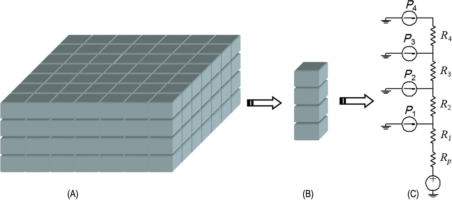
First order analysis of the thermal behavior of 3-D systems can be performed through the use of one-dimensional (1-D) thermal models. An example is depicted in Fig. 12.1B. This thermal model is accurate if the flow of heat moves exclusively along the z-direction. The assumption of 1-D heat flow is justified by the short height of the 3-D stack and because the lateral boundaries of a 3-D IC are considered to behave adiabatically. Although thermal models based on analytic expressions exhibit the lowest accuracy, these models provide a coarse estimate of the thermal behavior of a circuit. This estimate may be of limited value at later stages of the design process where more accurate models are required; however, analytic models are useful during the early stages of the design process where physical information describing the circuit does not yet exist. These first order models are used to determine several design characteristics, such as packaging and cooling strategies and estimates of overall system cost [459].
In a 1-D thermal model, each material layer is modeled as a thermal resistor, heat sources as current sources, and temperature differences as voltage differences. An example of the relevant expressions describing the transfer of heat based on this model for a three tier 3-D circuit is shown in Fig. 12.3. The thermal equations resemble Kirchhoff's voltage law (KVL) expressions, as shown in the right half of the figure. This duality between the flow of current and of heat is extensively employed for thermal analysis both in first order analytic expressions and more elaborate models [444], as discussed in later sections of this chapter. To determine the temperature of the tiers based on this model, as shown in Fig. 12.3, the heat generated within each tier and corresponding thermal resistances need to be determined.

A simple approach to model a 3-D system, with a structure as shown in Fig. 12.1A, is a cube consisting of multiple layers of silicon, aluminum, silicon dioxide, and polyimide. As depicted in Fig. 12.4, each layer is a homogeneous layer with a constant thermal conductivity. The devices on each tier are treated as isotropic heat sources and modeled as a thin layer on the top surface of each silicon layer. Either the top or bottom surface of the 3-D circuit is assumed to be adiabatic, although a non-negligible portion of the generated heat flows to the ambient through this surface. More detailed models also include the flow of heat through this surface. Alternatively, the other side of the 3-D IC, which is typically connected to a heat sink, is treated as an isothermal surface. These conditions simplify the analysis, as only a small set of important parameters needs to be investigated. Closed-form expressions also support fast design exploration as the size of the problem is reduced to only a few design parameters. The objective of these models is not to address circuit performance issues due to high temperatures but rather system level decisions; for example, the package, die stacking order, cooling mechanism, heat spreading materials, package level interconnects, and other system wide parameters that affect the design and cost of the overall system.

The heat generated within the silicon layers is primarily due to the transistors. Self-heating of the metal oxide semiconductor field effect transistor (MOSFET) devices can also cause the temperature of a circuit to rise significantly. Certain devices can behave as hotspots, causing significant local heating. For a two tier 3-D structure, an increase of 24.6°C is observed due to the silicon dioxide and polyimide layers acting as thermal barriers for the flow of heat towards the heat sink [441]. Although the dielectric and bonding layers behave as thermal barriers, the silicon substrate of the upper tiers spreads the heat, reducing the self-heating of the MOSFETs. Simulation results indicate that by reducing the thickness of the silicon substrate from 3 to 1 μm in a two tier 3-D IC, the temperature rises from 24.6 to 48.9°C [441]. Thicker silicon substrates, however, decrease the packaging density and increase the length of the intertier interconnects. In addition, high aspect ratio vias can be a challenging fabrication task, as discussed in Chapter 3, Manufacturing Technologies for Three-Dimensional Integrated Circuits. If the silicon substrate is completely removed, as in the case of 3-D silicon-on-insulator (SOI) circuits, self-heating can cause the temperature to rise to 200°C, which can catastrophically affect the operation of the ICs. In this model, the interconnects (BEOL) are implicitly included by considering a specific aluminum density within a dielectric layer, as depicted in Fig. 12.4. This situation is described by
(12.12)
where kox and kmetal are, respectively, the thermal conductivity of the intralayer dielectric and interconnect metal and dw is the interconnect density. This expression does not consider the several thermal paths that exist within the BEOL within each tier and does not differentiate between horizontal and vertical wires and metal contacts. Rather, an average thermal conductivity is determined by recognizing that a part of the volume of each BEOL layer consists of a dielectric (1–dw) while the rest of the volume consists of metal dw. This notion of an effective thermal conductivity is extensively utilized throughout the literature. For example, the TSV density within the silicon substrate is included to determine an average thermal conductivity within the substrate. This averaging is a convenient way to simplify the thermal analysis process, although in certain cases averaging can lead to significant inaccuracy, as discussed in later sections of this chapter.
To estimate the maximum rise in temperature on the upper tiers of a 3-D circuit, similar to that shown in Fig. 12.4, a simple closed-form expression based on 1-D heat flow has been developed, consistent with the thermal circuit illustrated in Fig. 12.1B. Consequently, the temperature increase ΔTj at the tier j of a 3-D circuit modeled as in Fig. 12.4 can be described by
(12.13)
where Pk/A and Rk are, respectively, the power density of tier k and the thermal resistance from k to the ambient. The power density does not include interconnect joule heating, while the heat removal properties of the interconnects are only implicitly included in Rk.
Assuming the same power consumption and thermal resistance for all but the first tier, which is valid for a homogeneous 3-D circuit such as a memory cube, the increase in temperature is [458]
(12.14)
The thermal resistance of the first tier includes the thermal resistance of the package and the silicon substrate,
(12.15)
where tSi1 and tpkg are the thickness and ksi and kpkg are the thermal conductivity of, respectively, the silicon substrate of the first tier and the package. The thermal resistance of an upper tier k is
(12.16)
where tsik, tdielk, and tifacek are the thickness and kSik, kdielk, and kifacek are the thermal conductivity of, respectively, the silicon substrate, dielectric layers, and bonding interface for tier k. From (12.14) to (12.16), the increase in temperature on the topmost tier for different number of tiers and power densities of a 3-D system is illustrated in Fig. 12.5 for a typical thickness and thermal conductivity of the substrates, dielectrics, and bonding materials. As shown in Fig. 12.5, the increase in temperature exhibits a square dependence on the number of tiers and a linear relationship with the power density. Note that the thermal resistance of the package (or, equivalently, the junction thermal resistance in (12.5)) provides the greatest contribution to the increase in temperature. Further to this point, more recent results have shown that the choice of heat sink and package can change the purely monotonic increase in temperature with the number of tiers. If the boundary condition of the top surface being adiabatic is relaxed, the heat flows through both the top and bottom surfaces of a 3-D stack (i.e., package and heat sink) and, depending on the thermal resistance of the package and heat sink, the tier with the highest temperature is not always the tier farthest from the heat sink (or, alternatively, closest to the package). Rather, the temperature within the stack increases monotonically up to some tier and decreases for the remaining planes. For a two tier 3-D system, for the structure shown in Fig. 12.1, the second tier can exhibit a higher temperature if the following condition applies [459],
(12.17)
where khs is the thermal conductivity of the heat sink. From Fig. 12.5, the temperature within a 3-D circuit is exacerbated even for a small number of tiers. The effect of the interconnects on removing the heat is not explicitly described, and interconnect joule heating has not been incorporated into these expressions. The increase in temperature on a specific tier k within a 3-D circuit considering the heat removal properties of the interconnect and the rise in temperature due to interconnect joule heating is described by [460]
(12.18)
where the first term represents the temperature increase from the interlayer dielectrics (ILDs), while the second term yields the rise in temperature caused by the package, the bonding materials, and the silicon substrate(s). The notations in (12.18) are defined in Table 12.2. Expression (12.18) considers a 1-D model of the heat flow within a 3-D system similar to that based on Fig. 12.4 but applies a more accurate model of the different thermal conductivities and heat sources as compared to (12.14) to (12.16).

Table 12.2
Definition of the Symbols Used in (12.18)
| Notation | Definition |
| Tamb | Ambient temperature |
| n | Total number of tiers |
| Ni | Number of metal layers in the ith tier |
| ir | rth interconnect layer in the ith tier |
| tILD | Thickness of ILD |
| kILD | Thermal conductivity of ILD materials |
| sf | Heat spreading factor |
| η | Via correction factor, 0≤η≤1 |
| jrms | Root mean square value of current density for interconnects |
| ρm | Electrical resistivity of metal lines |
| Η | Thickness of interconnects |
| Φm | Total power density on the mth tier, including the power consumption of the devices and interconnect joule heating |
| R1 | Total thermal resistance of package, heat sink, and Si substrate (bottom tier) |
| Ri (i>1) | Thermal resistance of the bonding material and the Si substrate for each tier |
By including intertier vias and interconnect joule heating in the thermal model of a 3-D system, the thermal behavior of a 3-D circuit can be more accurately modeled. The rise in temperature of a two tier 3-D system is evaluated for two scenarios. In one scenario, interconnect joule heating and intertier vias are not considered, while in the second scenario, interconnect thermal effects are included. A decrease of approximately 40°C in the temperature of the bottom Si substrate is observed in the second scenario as compared to the first scenario. This result is an early indication of the important role that intertier vias play on reducing the overall temperature of a 3-D system by decreasing the effective thermal resistance in the vertical direction.
Although (12.18) includes the effect of the interconnect on the heat flow process (as a BEOL layer within the stack), the several heat transfer paths that can exist within the interconnect structures require investigation. For example, assuming 1-D heat flow, heat is only transferred vertically within the intratier metal layers. Due to physical obstacles such as circuit cells or routing congestion, a continuous vertical path may not be possible for certain interconnections. This situation is depicted in Fig. 12.6 where different thermal paths are illustrated. As with current flow, heat flow also follows the path of the highest thermal conductivity. Consequently, interconnections consisting of horizontal segments in addition to intertier vias cause the heat flow to deviate from the vertical direction and spread laterally over a certain length, depending upon the length and thermal conductivity of each thermal path. By considering several thermal paths that exist within the BEOL layers, as shown in Fig. 12.6, the effective thermal conductivity of the buried interconnect layer consisting of a dielectric and metal is [461]
(12.19)
where tbi and Aint are, respectively, the thickness of the interconnect layer and the area of the buried interconnect layer. The thermal resistance of the paths is given by Ri, where these paths are considered in parallel, similar to electrical resistors connected in parallel. This duality implies that the presence of multiple thermal paths in a region produces a change in the total thermal conductivity of that region as compared, for example, with the thermal conductivity described by (12.12). By considering the different parallel thermal paths that can exist along the metal layers of each physical tier, a more accurate model of the flow of heat within the BEOL is achieved, although a single thermal resistor is utilized to characterize the entire layer.

As high temperatures can affect the reliability of a circuit, early publications on thermal analysis of 3-D circuits employing these first order models investigated self-heating of these devices [461]. Primary candidates include those devices that exhibit a high switching activity, such as clock drivers and buffers [461], which can suffer greatly from local heating, resulting in degraded performance. By considering the various thermal paths that can exist within interconnect structures, the effect of a rise in temperature on these devices has been investigated [461]. The increase in peak temperature as a function of the power density of the clock drivers placed above different interconnect structures is illustrated in Fig. 12.7. The existence of a thermal path with a horizontal metal segment exhibits inferior heat removal properties as compared to an exclusively vertical thermal path. In addition, the resulting increase in temperature in a 3-D IC is higher than bulk CMOS but not necessarily worse than SOI, as illustrated in Fig. 12.7.

Another factor that can affect the thermal profile of a circuit is the physical adjacency of the devices. Thermal coupling among neighboring devices within a 3-D circuit is greater as proximity increases, further increasing the temperature of the circuit [441,461]. The temperature is shown to exponentially decrease with gate pitch. This behavior implies that the area consumed by certain circuit elements, such as a clock driver, should be greater in a 3-D circuit than in a 2-D circuit to guarantee reliable operation by lowering thermal degradation.
The assumption of 1-D heat flow permits a circuit to be modeled by a few serially connected resistors. Additionally, by including the interconnect power and the different thermal paths by appropriately adapting the thermal conductivity of some layers, the accuracy of the thermal models of 3-D ICs is significantly improved. The major assumption, and simultaneously, primary drawback of the closed-form expressions describing the temperature of a 3-D circuit is that each physical tier is characterized by a single heat source. This assumption implies that all of the heat sources that can exist within a tier collapse to a single heat source, as depicted in Fig. 12.3. Consequently, phenomena such as thermal coupling and intratier thermal gradients cannot be captured. Thus, although this approach is sufficiently accurate during early steps in the design process, knowledge of the actual power density and temperature within each physical tier is essential to thermal design methodologies to maintain thermally tolerant circuit operation. More accurate models required for these techniques are presented in the following subsection.
12.3 Mesh-Based Thermal Models
1In the previous subsection, thermal models based on analytic expressions to evaluate the temperature of a 3-D circuit are discussed. In all of these models, the heat generated within each physical tier is represented by a single value. Consequently, the power density of a 3-D circuit is assumed to be a vector in the vertical direction (i.e., z-direction). In addition, the thermal network is represented as a 1-D resistive network, as shown in Fig. 12.1B.
The temperature and heat flow within each tier of a 3-D system, however, can fluctuate considerably, yielding temperature and power density vectors that vary in all three directions. Mesh-based thermal models capture this critical information by representing the volume of a circuit with a set of tiles. Each tile is thermally modeled with a small number of resistors (and capacitors if the thermal transient behavior is also analyzed), as illustrated in Fig. 12.8. The tiles are connected through nodes at the tile boundaries forming a 3-D thermal network, where the temperature at each node is determined. Although in this figure only two different thermal resistances are indicated, Rz and Rxy, which relate to the transfer of heat in, respectively, the vertical and horizontal directions, all resistances can be different. In addition, some elements may not be included in each tile. For example, if no heat is generated within a cell, the current source can be omitted. If only a steady-state analysis is intended, the capacitors are not required. Furthermore, a resistor in the vertical direction is not included in the case of the topmost/bottommost tier of the stack. Therefore, which elements are present in each tile depends not only on the components of the 3-D stack within each cell but also on the intended analysis. Similar to the R(L)C extraction process for IC layouts, the thermal components within the volume of each tile must be extracted. This process, however, is not straightforward as typically the volume of a tile contains different materials. In other words, the tiles are not in general homogeneous. For example, a tile may include some segment of a wire, interlayer dielectric, metal contacts, some diffusion area, a TSV, and/or silicon. The volume of the tiles can become arbitrarily small yet finite, ensuring that each tile contains only one material, making the thermal elements more easily determined. This approach, however, greatly increases the number of cells and, consequently, the number of nodes that needs to be analyzed, rendering the computational time impractical. A characteristic example is the use of multiphysics solvers, which can practically analyze only the smallest 3-D [462,463]. Thus, researchers have resorted to approximations to reduce the number of tiles needed to characterize a 3-D circuit. Based on these experimental results and comparisons between multiphysics solvers and proposed approximations, tiles with dimensions on the order of tens of micrometers are computationally practical while offering reasonable accuracy [449,464].

Tiles of this scale can contain interconnects, dielectrics, and/or silicon, as the feature size of modern technology nodes is on the scale of nanometers. Consequently, several methods have been developed to determine the thermal components of the tiles. The majority of the methods emphasize thermal resistance as most of these techniques focus on steady-state analysis. The current source is typically the current passing through the transistors within the cell or equivalently, the heat generated by the current flowing through the wires for those tiles within the BEOL layers.
An early model, a compromise between a 1-D thermal circuit and a full mesh, models a 3-D system as a thermal resistive stack, as shown in Fig. 12.9. The discretized volume of the system shown in Fig. 12.9A is segmented into single pillars, as illustrated in Fig. 12.9B [465–467]. Each pillar is successively modeled by a 1-D thermal network including thermal resistors and heat sources, as shown in Fig. 12.9C. The heat sources include all of the heat generated by the devices contained within each tile. Resistances related to the TSV are also included in the pillar. The absence of a TSV between two tiers is incorporated by removing the via resistances, ensuring that heat will not flow through those resistors. The voltage source at the bottom of the network models the isothermal surface between the heat sink and the bottom silicon substrate. Additional resistors, not shown here, can be used to incorporate the flow of heat among neighboring pillars.
Comparing the compact model of a single pillar of the stack with the simpler 1-D model used to produce the closed-form solution presented in Section 12.2, several similarities exist. Both of these models use resistors and heat sources modeled as current sources. Note that although the voltage source included in Fig. 12.9C, which considers the heat sink, does not appear in Fig. 12.3, this element of the model is implicitly included in (12.18) as the closed-form expression describes the rise in temperature in tier k of a 3-D system (i.e., ΔT=Tsi_N–Tamb) rather than the absolute temperature generated by a compact 1-D model.
Merging several cells into a pillar reduces the number of nodes at which the temperature needs to be determined, thereby reducing the computational complexity of the problem. The accuracy, however, may be degraded. In addition, this model has been developed for a specific technology and cannot be used to explore different technologies where physical characteristics differ. The usefulness of a model depends not only on the complexity which is related to the number of parameters that need to be determined but also on the capability of the model to support different geometries and fabrication parameters since 3-D integration is manifested in diverse manufacturing processes. In addition, this model does not describe the disparate materials that can exist within a cell other than a TSV.
In 3-D systems, the primary direction where the heat flows is vertical. Accurately modeling the direction of the thermal behavior of the TSVs is highly important, as the TSVs provide a path of high thermal conductivity along this vertical direction. Thus, a non-negligible number of works has been developed to thermally model the TSVs [465–471]. Due to enhanced heat conduction properties, TSVs have also been used solely for the purpose of facilitating the flow of heat. These heat conduits are called thermal TSVs (TTSVs) and several thermal management techniques have been developed to allocate these resources across the volume of a 3-D system, ensuring the resulting system satisfies the temperature specifications. Consequently, different models exist for signal and TTSVs, where the TTSVs are not subject to joule heating as no current flows through these vias.
An alternative cooling approach that makes obsolete the need for TTSVs and supports more efficient heat removal is that of integrated liquid cooling, as discussed in Section 12.1.1. As the presence of fluid flow adds a convective component of heat transfer, the modeling process for microchannels is not the same as within solids where conduction is the primary mechanism of heat transfer. Consequently, the unit cells within a discretized 3-D system describing a microchannel need to be modeled differently as compared to the volume of a solid, as shown in Fig. 12.8. In the next subsections, thermal models of varying complexity for different types of TSVs and fluidic channels are discussed.
12.3.1 Thermal Model of Through Silicon Vias
The simplest thermal model of a TSV is a resistor (similar to (12.15)) equal to the inverse of the thermal conductivity km of the metal used for the TSVs (typically copper or tungsten) and the area of the TSV ATSV, and multiplied by the length of the TSV tTSV or, alternatively, the length of the cell (where the cell contains only part of the TSV),
(12.20)
This model, however, neglects several important aspects which affect the model accuracy. For example, joule heating is excluded and the non-negligible lateral flow of heat through the TSV liner is not considered. In addition, the case where multiple TSVs are included within a single cell requires a different modeling approach. These aspects are discussed in the following subsections.
12.3.1.1 Thermal through silicon vias
As previously mentioned, TTSVs act exclusively as heat pipes, allowing heat to flow to the heat sink, alleviating hotspots within a 3-D stack. Early thermal management techniques modeled TTSVs as a single resistance, ignoring lateral heat transfer effects. However, lateral flow of heat should not be neglected as this mechanism affects the overall heat transfer process. Although the thermal conductivity of the surrounding dielectric of the TSV liner is considerably lower than that of silicon and metal, the liner thickness is typically about a micrometer. Due to this short thickness, heat flows laterally towards the thermally less resistive metallic TSV, facilitating the heat removal process through the 3-D stack. Assuming a cell includes a TSV within the silicon substrate, as shown in Fig. 12.10, the different physical parameters of the TSV typically used in thermal models are considered. The simulation setup to determine the thermal conductivity along the path of the flow of heat is depicted in Fig. 12.11. The structure illustrated in Fig. 12.11A applies a heat source at the left boundary surface, while the top and bottom surfaces are adiabatic. In a similar way, a heat source is applied at the top surface in Fig. 12.11B while the lateral walls are considered adiabatic. Auxiliary blocks (see Fig. 12.11B) are added to ensure that the heat spreads uniformly before reaching the target cell, and a small section ΔH is evaluated to determine the local thermal conductivity. Note that this small segment includes only part of the TSV, liner, and silicon substrate, which is not necessarily consistent with larger cells since these larger cells often include other materials. From this perspective, two distinct thermal conductivities are determined along the xy-plane and z-direction through the following expressions [468],
(12.21)
(12.22)
(12.23)
(12.24)
(12.25)
(12.26)
where ![]() is the thickness of the silicon dioxide (or another dielectric) layer surrounding the TSV, and DTSV, P, and H are, respectively, the diameter, pitch, and height of the TSV. These expressions are applicable for a range of these parameters: liner thickness of 0.2 to 2.0 μm, TTSV diameter of 10 to 50 μm, TTSV length greater than 20 μm, and 0.1≤DTSV/P≤0.77. These expressions are compared with simulations from the Icepak solver [463] and the error is less than±10%.
is the thickness of the silicon dioxide (or another dielectric) layer surrounding the TSV, and DTSV, P, and H are, respectively, the diameter, pitch, and height of the TSV. These expressions are applicable for a range of these parameters: liner thickness of 0.2 to 2.0 μm, TTSV diameter of 10 to 50 μm, TTSV length greater than 20 μm, and 0.1≤DTSV/P≤0.77. These expressions are compared with simulations from the Icepak solver [463] and the error is less than±10%.


This model, however, only considers that segment of the TSV within the silicon substrate, which is not the case for TSV-last processes. In addition, the thermal conductivity in these expressions is either an exponential, parabolic, or logarithmic function depending upon the value of certain physical parameters, without offering any intuitive insight. To consider those parts of a TTSV through the bonding and BEOL layers, for example, and to offer a more intuitive model of a TTSV, another model that employs three thermal resistances per TTSV has been developed. The rationale behind this model is based on the three major heat transfer paths witihin a volume of a 3-D stack that includes a stacked set of TTSVs. A stacked TTSV is a better option for removing heat as a continuous structure has the least thermal resistance and removes heat more efficiently. Consequently, employing stacked TTSVs is a reasonable practice to facilitate the vertical flow of heat.
For the structure shown in Fig. 12.11, a small volume of a 3-D system is evaluated with COMSOL [462]. This volume corresponds to a segment of a three tier 3-D circuit with a single TTSV, which can be extended to an n-tier circuit. The physical structure of this stack is illustrated in Fig. 12.12A. The cross-section of the circuit and the temperature distribution determined from COMSOL multiphysics are illustrated in Fig. 12.12B. Although for different fabrication technologies the materials and geometries of the circuit can vary, the underlying structure remains the same. This model is based on a 3-D technology employing wafer bonding. As labeled in Fig. 12.12A, each tier of the circuit consists of three layers describing, respectively, the silicon substrate (Si), the interlayer dielectric (ILD) and metal interconnects (i.e., BEOL), and the bonding layer. The heat sources include the power generated by the active devices on the top surface of the Si substrates and Joule heating due to the interconnects surrounded by the ILD.

As shown in Fig. 12.12, three major paths of heat flow are illustrated. Heat flows vertically through silicon (path 1) and the TTSV (path 3) and laterally through the liner of the TSV (path 2) towards the more conductive metal fill within the TTSV. The flow of heat along each of these paths can be modeled by a resistance. If the model is intended to support design exploration, the model should be linked with the physical characteristics of the TSV including, for example, the thickness of the liner and diameter of the TSV. As the heat transfer process can be more complicated (there are many more paths in addition to these three paths), some fitting coefficients are used to improve the accuracy of the model. Based on these heat flow paths, the following expressions describe the thermal resistance of each TSV,
(12.27)
(12.28)
(12.29)
(12.30)
(12.31)
(12.32)
(12.33)
(12.34)
(12.35)
(12.36)
where tb and tSin are the thicknesses of, respectively, the bonding layer and the substrate for tier n. The thermal conductivity of the TSV and the liner are notated, respectively, by kTSV and ![]() . In (12.27)–(12.36), the resistances, R2, R5, and R8, are the thermal resistances of the filling material (e.g., copper) of the TTSV. R2 describes the resistance of the TSV for the first or last tier, where the TSV may be “blind” (i.e., enclosed within the substrate) and, consequently, lext is employed to capture this case. In addition, there is no bonding layer for this tier, therefore, this term is omitted from (12.28). The resistances R3, R6, and R9 denote the lateral thermal resistance of the insulator liner (e.g., SiO2) of the TTSV. The resistances R1, R4, and R7 denote the thermal resistance of the TTSV surroundings (see Fig. 12.13) for each of the three physical tiers. The thermal resistance of the silicon substrate of the first tier is denoted by Rs due to the considerably different thickness of the substrate (note that a separate resistance is also added for the tier with the thick silicon substrate in the model shown in Fig. 12.9C). Although this model captures more of the technological characteristics of a 3-D system, two fitting coefficients k1 and k2 are required for the model to provide sufficient accuracy with an average and maximum error of, respectively, 3% and 6% for the investigated scenarios [469]. The k1 and k2 coefficients adjust the lumped model representation of the thermal resistance of the TTSV when used with a distributed model of heat flow.
. In (12.27)–(12.36), the resistances, R2, R5, and R8, are the thermal resistances of the filling material (e.g., copper) of the TTSV. R2 describes the resistance of the TSV for the first or last tier, where the TSV may be “blind” (i.e., enclosed within the substrate) and, consequently, lext is employed to capture this case. In addition, there is no bonding layer for this tier, therefore, this term is omitted from (12.28). The resistances R3, R6, and R9 denote the lateral thermal resistance of the insulator liner (e.g., SiO2) of the TTSV. The resistances R1, R4, and R7 denote the thermal resistance of the TTSV surroundings (see Fig. 12.13) for each of the three physical tiers. The thermal resistance of the silicon substrate of the first tier is denoted by Rs due to the considerably different thickness of the substrate (note that a separate resistance is also added for the tier with the thick silicon substrate in the model shown in Fig. 12.9C). Although this model captures more of the technological characteristics of a 3-D system, two fitting coefficients k1 and k2 are required for the model to provide sufficient accuracy with an average and maximum error of, respectively, 3% and 6% for the investigated scenarios [469]. The k1 and k2 coefficients adjust the lumped model representation of the thermal resistance of the TTSV when used with a distributed model of heat flow.

A method to eliminate fitting coefficients while not degrading accuracy is to model the TTSV with additional resistors. The stack (or single) TTSV is modeled as a distributed resistive wire. This situation means that additional cells are used to model the target volume, which naturally improves the precision without the need for fitting coefficients but increases the computational complexity. Thus, for the volume shown in Fig. 12.12A, a comparison between the distributed and lumped models is performed, where the reference temperatures are the results reported by an finite element method (FEM) solver [462]. The results listed in Table 12.3 indicate that more than a hundred segments can have an undesirable overhead on the computational time [469]. Alternatively, the overhead for producing the fitting coefficients for specific structures is performed only once and may be a more computationally efficient method for thermal analysis without sacrificing accuracy (model A in Table 12.3). An example of the usefulness as well as accuracy of this model is given in Fig. 12.14, where the maximum rise in temperature for a three tier circuit is plotted as a function of the thickness of the liner (e.g., ![]() ). Note that the 1-D model cannot capture this temperature increase, while the accuracy of the distributed model marginally improves when more than 100 segments are utilized.
). Note that the 1-D model cannot capture this temperature increase, while the accuracy of the distributed model marginally improves when more than 100 segments are utilized.
Table 12.3
Error and Computational Time Versus Number of Segments in the Distributed Model
| Model (# of Segments) | B (1) | B (20) | B (100) | B (500) | A | 1-D |
| Max. error | 23% | 12% | 6% | 5% | 4% | 30% |
| Avg. error | 19% | 11% | 4% | 3% | 2% | 23% |
| Time (ms) | 1 | 3 | 32 | 2474 | – | – |


 =7 μm, tb=1 μm, tSi2=tSi3=45 μm, k1=1.3, and k2=0.55.
Inclusion of the lateral path more accurately describes the flow of heat and reduces overdesign. If excluded, typically higher temperatures are predicted, which, in turn, require more demanding thermal management schemes. To illustrate this situation, a DRAM memory-processor system has been analyzed employing this model and a 1-D model (only one resistor models a TSV as in [459]), and is compared with FEM simulation. The maximum rise in temperature for the more complex model, 1-D model, and FEM is, respectively, 12.8, 20, and 12°C, exhibiting the high inaccuracy introduced by ignoring the lateral flow of heat through the liner.
Both of the models discussed in this section require some fitting to enhance accuracy. In the first model, this fitting is achieved by changing the form of the function describing the thermal conductivity. This approach, however, offers limited insight into the dependence of the flow of heat on the physical parameters, such as the radius of the TSV. The second model uses certain fitting coefficients to improve precision. The resulting inaccuracy depends upon the ratio of the TSV radius to the TSV pitch. This ratio causes bending in the isothermal curves among adjacent TSV cells, as shown in Fig. 12.15. For a similar range of DTSV/P (i.e., [0.125 to 0.25]) as in [468], a correction factor models the bending of the isothermal curves under the presence of identical cells. Thus, the model used in [470] magnifies the thermal resistance of a TTSV with a corrective factor θ, which is a linear function of the TSV space-to-radius ratio, δ=2(P-DTSV)/DTSV. This function is
(12.37)
where β1 and β2 are fitting coefficients which can be determined from either simulated or measured data with linear fitting techniques [470].

In general, a structure with juxtaposed TSV cells is not applicable, as the adjacent cells may not contain any TSVs and, consequently, the heat will flow in different ways. Arrays of TTSVs are typically used to mitigate thermal hotspots. The rationale behind the use of these TTSV arrays is that the effective thermal conductivity increases in this local region, lowering the high temperatures. Since these TTSV arrays require non-negligible area, models that include more than one vertical path for the heat to flow lead to fewer TTSVs and are therefore a useful means to limit this area overhead while also satisfying thermal limits [469].
12.3.1.2 Signal through silicon vias
Although some models have been published for TTSVs, there are few models that capture the thermal behavior of signal TSVs, where the primary difference is that heat is generated within these TSVs (joule heat) due to the current flowing through those wires. In addition, as the current flowing through the TSV is not constant (even for power/ground TSVs), the transient thermal behavior of the target cell must be considered. For a basic structure, such as the tapered TSV shown in Fig. 12.16, commercial multiphysics solvers, such as COMSOL, can be employed to analyze the thermal behavior of this cell. Another reasonably efficient approach for multiphysics characterization of TSVs is the hybrid time-domain finite-element method [471].

The thermal resistance of a tapered TSV including the lateral flow of heat through the liner and the contribution of the starting and landing pads is described by
(12.38)
where the notation of the different physical traits are illustrated in Fig. 12.16. Note that this expression includes the contribution of the resistance of the starting and landing pads of the TSV in addition to the metal fill of the TSV. Hence, the diameter of the pads Dpad is included in the second term of the expression. To determine the transient thermal behavior, a periodic trapezoidal signal pulse is applied at the top of the TSV (the opposite situation can also occur, should the signal propagate upwards through the stack), and the transient temperature of the TSV is observed. The oxide thickness is an important factor in evaluating the transient thermal response of the TSV. This situation also applies for the case of stacked TSVs [471]. Although stacked signal TSVs are infrequent due to routing constraints, TSVs for power and ground distribution networks are usually placed at the periphery of a tier (or circuit blocks within a tier) stacked across several physical tiers [472]. In addition, a thinner oxide increases the lateral flow of heat, although the electrical capacitance of the TSV increases. In addition, the tapering of a TSV affects the temperature distribution across the length of the TSV, where the highest temperature appears at the bottom of the TSV with the smallest cross-section. Finally, interactions between the electrical and thermal characteristics of the TSV must be considered due to the dependence of the electrical resistance on temperature.
Before completing the discussion of TTSV models, note that this analysis is based on the assumption that specific material properties, such as the thermal conductivity, are constant. This assumption facilitates solving the related expressions but can overestimate the rise in temperature within a TSV. To investigate the deviation of the resulting temperatures due to the assumed independence of the thermal conductivity, an analysis of a single TSV has been performed assuming material properties independent of temperature. The temperature is overestimated by up to 5.7% for ![]() =20 nm, while this divergence increases to 15.2% for
=20 nm, while this divergence increases to 15.2% for ![]() =100 nm [471]. The overestimate in temperature is attributed to the increased conductivity of the liner. Although the conductivity of the substrate decreases, the overall effect is a decrease in temperature [471]. In this analysis, the thermal conductivity of the metal fill, liner, and silicon substrate is approximated as a fourth order polynomial of temperature T,
=100 nm [471]. The overestimate in temperature is attributed to the increased conductivity of the liner. Although the conductivity of the substrate decreases, the overall effect is a decrease in temperature [471]. In this analysis, the thermal conductivity of the metal fill, liner, and silicon substrate is approximated as a fourth order polynomial of temperature T,
(12.39)
where x(T) is the material property approximated by the polynomial, ci is the corresponding coefficients, and T0 and T1 limit the temperature range for which this approximation is valid. These coefficients are listed in Table 12.4 for different material and temperature ranges.
Table 12.4
Polynomial Coefficients for Temperature Dependent Material Parameters [471]
| Material Coefficients | Metal Fill | Liner | Bonding | |||
| Cu | Tungsten (W) | Poly-Si | Silicon | SiO2 | BCB | |
| kCu(T) | kW(T) | kPoly-Si(T) | kSi(T) | kBCB(T) | ||
| c0 | 420.33208 | 191.23977 | 441.10556 | 332.14097 | 0.54335 | 0.08511 |
| c1 | −0.06809 | −0.07538 | −4.71735 | −1.07848 | 0.00105 | 6.96767×10⁻⁴ |
| c2 | 0 | 0 | 0.02008 | 0.00158 | 0 | 0 |
| c3 | 0 | 0 | −3.76157×10⁻⁵ | −1.08505×10⁻⁶ | 0 | 0 |
| c4 | 0 | 0 | 2.60417×10⁻⁸ | 2.81425×10⁻¹⁰ | 0 | 0 |
| Applicable temperature range (K) | (200, 1200) | (300, 1000) | (300, 400) | (300, 1300) | (273, 1000) | (297, 339) |

All of the models discussed in this section include a different number of elements as compared to the typical unit cell structure shown in Fig. 12.8. Standard transformations can be used to map these models to a six resistor cell model [473]. Thermal models of channels for liquid cooling in 3-D systems are described in the following subsection.
12.3.2 Thermal Models of Microchannels for Liquid Cooling
A conceptual drawing of intertier integrated cooling with channels etched within the substrate of the tiers is illustrated in Fig. 12.2. Once the structure of the heat sink is determined, the thermal behavior of the liquid flowing through the microchannels can be modeled. The important difference for thermal modeling of a 3-D system that employs liquid cooling is that the greatest portion of the generated heat is removed through convection. Considering (12.6) for the thermal resistance of the heat sink, a thermal model of one channel includes all three resistive components, where fully developed hydrodynamic and thermal flow is assumed.
The partial volume of a discretized microchannel along with the surrounding walls is shown in Fig. 12.17, where the flow of the coolant is along the y-axis. The different thermal resistances are notated where, depending upon the fineness of the mesh, the resistances within one cell can vary. For example, if the size of a grid cell is equal to the cross-section of the channel, only convective and thermal capacity resistances should be considered. If the boundaries of a cell extend within the sidewalls, the conductive resistance should also be included. The magnitude of the resistances is determined by the expression, Rcond=t/(ksubAwall). The area of the solid which corresponds to the sidewall of the channel is Awall, and the thickness t is equal to the length of the edge of the solid segment in either the x- or z-direction. The resistance due to convection for cell i is
(12.40)
where ![]() and
and ![]() are, respectively, the temperature of the solid sidewall j within cell i and the temperature of the fluid. Qij is the heat transferred from the solid to the fluid. For full thermal flow, the temperature of the fluid within a cell can be considered constant in addition to assuming the same temperature for all of the walls of the channel within the cell i. To determine the convection resistance, the transfer coefficient h is determined from the Nusselt number (see (12.8)), which, in turn, can be determined by empirical relationships where the aspect ratio of the cross-section of the channel is treated as a variable [456,474]. Thus, the convection coefficient depends upon this aspect ratio. The total area of the walls is determined by the geometry of the channel. Once the Nusselt number is determined, the convection resistance is [475]
are, respectively, the temperature of the solid sidewall j within cell i and the temperature of the fluid. Qij is the heat transferred from the solid to the fluid. For full thermal flow, the temperature of the fluid within a cell can be considered constant in addition to assuming the same temperature for all of the walls of the channel within the cell i. To determine the convection resistance, the transfer coefficient h is determined from the Nusselt number (see (12.8)), which, in turn, can be determined by empirical relationships where the aspect ratio of the cross-section of the channel is treated as a variable [456,474]. Thus, the convection coefficient depends upon this aspect ratio. The total area of the walls is determined by the geometry of the channel. Once the Nusselt number is determined, the convection resistance is [475]
(12.41)
where the cell is assumed to contain the entire cross-section of the channel.

The third type of thermal resistance, which is due to the heat absorbed by the fluid flowing downstream from the channel, is [475]
(12.42)
which is considered constant throughout the length of a channel as a mean fluid velocity um is assumed and the cross-section is the same for all cells. The same resistance may be used for all of the channels if the assumption of a constant average fluid velocity is appropriate.
If the assumption of a constant heat flux is removed, these expressions no longer accurately describe the different resistances. This behavior is usually known as the “thermal wake effect” (i.e., the thermal trace due to the fluid flowing through the channel) [476]. For certain grid cells, the heat generated within the solid walls is transferred through the fluid to other cells downstream from the flow, adding to the thermal resistance of those cells. This phenomenon is qualitatively illustrated in Fig. 12.18. In addition, within the same cell, a heated segment of the substrate under the channel transfers heat to the sidewalls of the channel transverse to the fluid flow. To model this effect, the thermal model shown in Fig. 12.17B is augmented with a voltage controlled current source [477]. To better understand this situation, consider the rise in temperature within a cell id due to the thermal wake effect, as described by
(12.43)
where ![]() denotes the heat transferred to the fluid through transverse convection from a source cell is. The thermal wake function is treated as a transconductance denoted by
denotes the heat transferred to the fluid through transverse convection from a source cell is. The thermal wake function is treated as a transconductance denoted by ![]() . For those cells located farther downstream from the inlet location of the channel, more of these components are included to describe the cumulative nature of the thermal wakes. This situation implies that the added inaccuracy of not including the thermal wake effect in predicting the temperature of the fluid within the channel varies along the length of the channel. The temperature is, typically, overestimated for those cells located closer to the inlet of the channel and is underestimated for those cells located closer to the outlet of the channel (since the components of the thermal wake function accumulate downstream). Whether this effect should be included depends upon the status of the flow (developed vs. developing) and the desired accuracy of the model, as simulations exhibit an inaccuracy of up to ~10%, if the thermal wake effect is excluded from the thermal model.
. For those cells located farther downstream from the inlet location of the channel, more of these components are included to describe the cumulative nature of the thermal wakes. This situation implies that the added inaccuracy of not including the thermal wake effect in predicting the temperature of the fluid within the channel varies along the length of the channel. The temperature is, typically, overestimated for those cells located closer to the inlet of the channel and is underestimated for those cells located closer to the outlet of the channel (since the components of the thermal wake function accumulate downstream). Whether this effect should be included depends upon the status of the flow (developed vs. developing) and the desired accuracy of the model, as simulations exhibit an inaccuracy of up to ~10%, if the thermal wake effect is excluded from the thermal model.

Irrespective of the presence of liquid cooling, once the thermal elements of each cell are determined, the entire volume of a 3-D stack is converted into a mesh and appropriate analysis techniques can be used to determine the temperature at each node within the mesh. These techniques are presented in the following section.
12.4 Thermal Analysis Techniques
Methods for analyzing different heat transfer mechanisms have been investigated in the past and remain an active scientific topic. Thermal issues in integrated circuits have also been extensively studied over the past decades, where many well established techniques for thermal analysis have been explored and adapted to the specific traits of integrated circuits [478].
As discussed in Section 12.3, the entire volume of a 3-D system is discretized into a mesh. A 3-D mesh consisting of finite hexahedral elements (i.e., parallelepipeds), called cells, tiles, or control volumes, is illustrated in Fig. 12.19 (note that elements with different shapes can be utilized). The mesh can also be nonuniform for those regions with complex geometries or nonuniform power densities to provide either high accuracy or improve the computational time. A much finer mesh is often required at the interface of materials with greatly different conductivities. Alternatively, for a large volume of constant thermal conductivity, a coarser grid is a better choice as the analysis is computationally more efficient without affecting accuracy.

The volume of the circuit can be discretized with the use of several disparate methods, such as the FEM [479], finite difference [480,481], finite volume [482], and boundary element methods [439]. The thermal elements (e.g., heat generators and thermal resistors) connecting the vertices of the grid cells are modeled as discussed in the previous section. The vertices of the cells, typically called nodes or degrees of freedom, correspond to the unknown temperatures that are determined during the analysis process. Since most of the physical features within an integrated system are at the nanometer scale and each circuit includes millions of these cells, meshes with hundreds of millions of nodes can be produced. Once the volume of the system has been discretized and the thermal elements of the grid cells have been extracted, a matrix system describing the differential thermal expressions is obtained. This matrix system for a steady-state analysis (the objective of most methods) is a linear system of matrices of the form,
(12.44)
where G is the matrix of thermal conductance, T is the vector of temperature nodes that needs to be computed, and P is the vector containing the power sources of the system. Note that this matrix system is similar to that formed when solving for IR drops within power distribution networks [275]. Consequently, the duality of the thermal and electrical networks means that methods applied to the analysis of power distribution networks can also be adapted for thermal analysis. The resulting matrices are rather sparse. Appropriate techniques for solving sparse matrices are employed to decrease the computational time.
A number of techniques exist to solve the system of (12.44), where these methods are usually described as either direct or iterative solvers. Although the direct methods can produce high quality results for relatively small systems [482] (e.g., hundreds of thousands of nodes), the efficiency decays for large scale systems (e.g., multimillion nodes). Thus, scalability is a major issue for direct methods. Additionally, as the matrices of the system in (12.44) must be explicitly formed, the memory requirements can be significant.
An efficient means to improve the performance of direct or single level iterative solvers is to employ a nonuniform mesh to represent a 3-D system. A nonuniform mesh reduces the number of nodes to be solved and can be particularly helpful where different physical scales are required. This situation is encountered when the thermal behavior of a system simultaneously includes the 3-D circuit, package, and printed circuit board (PCB). The use of a nonuniform grid, however, must be carefully realized as the different cells can cause discontinuities at the interfaces, delaying convergence or causing the solver to diverge. Consequently, the interfaces between the different meshes must be treated carefully to establish continuity for the flow of heat throughout the entire system. The application of nonuniform grids has been compared to the use of a uniform mesh for a packaged integrated system mounted on a PCB [450]. The number of nodes decreases from 206,000 to 35,000 (6×) and the analysis time decreases by a factor of 91 [450].
Although the use of variable size meshes decreases the number of nodes or unknowns, direct solvers are not scalable. Alternatively, iterative methods can be more efficient, reducing both the computational time and the memory usage (12.44), where the most common (and powerful) iterative solvers are those based on multigrid methods [483]. In general, the computational complexity of multigrid techniques grows linearly (multiplied by a small constant) with the number of unknowns [483]. Another advantage as compared to other iterative schemes, such as the Gauss-Siedel method, is that multigrid solvers can efficiently remove the high frequency errors that can slow or hinder convergence in other methods. Due to these superior properties, multigrid methods have proven particularly efficient in solving these systems and, consequently, have been utilized with high success in a variety of different fields, such as fluid and molecular dynamics [484], in addition to electronic design automation.
Multigrid methods 1) construct coarser grids starting from an original fine grid, 2) solve the coarse grid, and 3) map and correct the coarse grid solutions with respect to the fine grid, where the process is repeated until the residue error reaches a predefined lower limit. This procedure is typically called a V-cycle [485,486] and is illustrated in Fig. 12.20. As depicted in this figure, a multigrid solving method requires a coarse grid operator, interpolation (for mapping the solution back to the fine grid), and restriction operators (for producing the coarse grid at the next level). A detailed treatment of multigrid methods can be found in several related publications [483,485,486]. Multigrid methods are divided into two categories: algebraic and geometric.

Although both methods have been employed in a large number of problems related to integrated circuits, geometric multigrid techniques have exhibited better performance. This enhanced performance is achieved since algebraic methods are applicable to more general problems and are, therefore, not readily adapted to the traits and requirements of integrated circuits. A specific difference between algebraic and geometric methods is that the former method utilizes fixed simple smooth functions and ensures convergence through complicated coarsening procedures, while the latter method uses specific smooth functions to implement effective smoothing and coarse grid correction as the hierarchy of the grid is fixed [487]. The choice of these operators plays a significant role in producing a robust and effective technique.
In addition, the grid hierarchy can be selected to ensure that the important characteristics of the system are not lost, thereby not degrading precision. In the case of integrated systems, irrespective of 2-D or 3-D, several thin layers exist, where the thermal conductivities can be quite different. This situation is typically relevant to the BEOL layers, which include dielectric and metal layers about 1 μm thick, while the silicon substrate is much thicker. A grid hierarchy based on coarsening all of the layers in all directions (x, y, z) often ignores important physical information describing these thin layers, delaying convergence. An appropriate choice, therefore, is to not coarsen the portion of the grid along the z-direction within the coarsening stages of the V-cycles [487]. This approach is shown in Fig. 12.21, and, although initially applied to a 2-D system, the same notion is applicable to a multi-tier 3-D structure. Another reason that also justifies this selective coarsening is the flow of the heat, as the primary heat conduction path within an integrated circuit is primarily along the z-direction. Since microchannel cooling is within the substrate, there is another major path where heat flows and, consequently, the grid hierarchy as well as the related coarsening and smoothing operators must be adapted to accommodate the existence of this second important thermal path [488].

The application of multi-grid methods has produced impressive reductions in both computational time and storage needs for both steady-state and transient state analysis [487,488]. As compared to the conjugate gradient method, thermal analysis of a planar circuit with ~2.5 million nodes has demonstrated a decrease in runtime and memory of, respectively, 420× and 32× while large circuits with ~12 million nodes are simply not solvable with non-multigrid methods [487].
The computational efficiency of multigrid techniques has been further improved through the use of GPU architectures [488]. The primary issue is to partition the solution process onto the underlying hardware architecture to best exploit the available computing resources (e.g., cores). The gains achieved from the resulting analysis procedure may, however, not be portable to other GPU architectures. Recent applications of multigrid methods to the thermal analysis of 3-D circuits including microchannel cooling of the nVIDIA Geforce GTX 285 GPU have demonstrated a 35× speed up over iterative solvers running on a quad core processor [488].
Other techniques have also been investigated for the thermal analysis of integrated circuits [489]. These methods are based on the Green’s function, the discretized form of which can be solved by spectral transformations such as the discrete cosine transform [490]. The use of these transformations, however, is suitable only for homogeneous layers. In the case of 3-D circuits, the TSVs within the silicon substrate produce discontinuities in the thermal conductance within the volume of the substrate. One approach is to employ an average thermal conductivity (an approach typically used in the closed-form models). This homogenization process however degrades accuracy irrespective of the efficiency of the analysis technique [491]. Moreover, the thermal effect of the TSVs is not accurately captured. One possible way to address this issue is to treat the TSVs as virtual power sources. Since the TSVs are replaced with virtual power sources, the substrate of each tier only consists of silicon; hence, the transformation used for 2-D circuits can also be utilized for a multi-tier stack. Modeling the TSVs as virtual power sources replaces the thermal conductivity of the TSVs in matrix G with the silicon substrate. Consequently, the thermal conductance matrix described by (12.44) is converted into two matrices which describe the homogeneous substrate without the TSVs and the difference between the TSV and substrate thermal conductivities [489]. The application of this method to a 3-D circuit has performed well over a finite difference solver, but the number of grid cells is on the order of several thousands [489]. Thus, scalability remains an issue for thermal analysis techniques based on the Green’s function.
Another technique that resembles solutions based on the Green’s function but removes the limitation for operating on homogeneous circuit regions is the “power blurring” technique, which originates from the field of image processing [492]. A digital image undergoes spatial filtering for certain operations, such as sharpening or blurring. To implement the blurring operation, the image f is convoluted with a matrix w, called a mask, as described by [493]
(12.45)
where a=(m−1)/2 and b=(n−1)/2 for a m×n matrix. Similarly, in the case of thermal analysis of integrated circuits, the power map of a circuit is convoluted with the response mask to obtain the thermal profile of the circuit. In the frequency domain, convolution corresponds to simple multiplication. The response mask represents a heat spreading function. For a unit source applied to a location within the circuit [492], the impulse response of this source provides one response mask. An illustration of the power blurring method is provided in Fig. 12.22. The application of (12.45) to a single response mask corresponds to the temperature distribution due to a single power source (whether this source corresponds to a single device or a circuit block depends upon the desired granularity of the analysis). Superposition is used to determine the overall temperature distribution across the entire power map of the circuit.

The performance of this method largely depends on the quality as well as number of response masks. The response masks correspond to the impulse response of the power sources and are determined prior to thermal analysis. Although any thermal analysis technique is applicable to this task, these methods use commercial tools, such as ANSYS, to produce the response masks. This setup task has proven to be computationally expensive and requires careful treatment to ensure that the computational load is appropriately balanced with the desired accuracy. An important issue is how many response masks are required. Early application of this method to planar circuits employs only a single response mask, where one heat source is present at the center of the circuit [492]. Another response mask can be applied at the edge of the circuit to include boundary effects, but the error introduced due to these effects can, alternatively, be eliminated by an added correction factor. Extraction of the response masks becomes more complicated when applied to 3-D circuits.
To produce a response mask, the rise in temperature in every tier due to the presence of a power source in one tier of the stack must be captured. As an example, if a two tier system is assumed, four response masks are required, which are noted as Mask11, Mask12, Mask21, and Mask22, where Maskxy denotes the response mask in tier x due to the presence of a heat source in tier y. The temperature profiles, T1 and T2, respectively, in tiers 1 and 2 are described by
(12.46)
(12.47)
where P1 and P2 are, respectively, the power map in tiers 1 and 2 [494].
Power blurring has been applied to a three tier circuit at a fine level of granularity (0.1 μm), where the circuit area is 3 mm×3 mm including about 714,000 power sources [491]. The computational time is significantly lower than analyzing the same system with a network of thermal resistors. Based on this case study, the crucial elements to broadly apply this technique relate to the computational resources and time required to produce the response masks, which can be a tedious process if applied for each transistor size and orientation of the transistor channel. To remedy a potentially intractable condition, the response mask for a group of transistors is utilized. This group accurately represents a set of standard cells if the physical characteristics of these groups are not very different [491]. This grouping process, however, is performed manually and consequently the efficiency of this practice depends strongly on design experience. Alternatively, the response masks can be determined only once for each thermal cell, and this information can be integrated within the design library.
Note that the discussion of these techniques does not favor one method over another method but, rather, highlights the advantages and limitations of these techniques. These techniques can also be used in a complementary and integrated manner, a path that has yet to be adequately explored. For example, multigrid thermal analysis at the circuit block level can indicate hotspots, and power blurring can be applied to small regions of a circuit with transistor level granularity to pinpoint (and alleviate) the most thermally fatigued devices.
12.5 Summary
Thermal models and related analysis techniques for 3-D ICs are discussed in this chapter. The primary concepts discussed in the chapter are
• High temperatures deteriorate circuit reliability and lifetime, increase leakage power, and decrease circuit performance.
• Higher temperatures and thermal gradients are predicted for 3-D ICs due to increased power densities and greater distances between the circuits on the upper tiers and the heat sink(s).
• Thermal coupling can further increase self-heating of devices, which leads to hotspots.
• Liquid cooling has been shown to effectively remove heat from 3-D circuits. The design of a microchannel heat sink requires careful design tradeoffs between the geometry of the channels and the characteristics of the off-chip cooling system. Manufacturing and electrical issues can further constrain the design of the heat sink.
• Thicker silicon substrates facilitate the conductive heat transfer process; however, high aspect ratio intertier vias reduce performance and are difficult to fabricate.
• Thermal models of 3-D circuits include analytic expressions, compact thermal resistive networks, and 3-D grids for numerical analysis. The models are listed in ascending order of increasing computational complexity and accuracy.
• A first order analysis of thermal behavior of 3-D systems can be performed with 1-D thermal circuits, where a thermal circuit is appropriate if the flow of heat is assumed to occur exclusively in the z-direction. In a 1-D model, each material layer is modeled as a thermal resistor, heat sources as current sources, and temperature differences as voltage differences.
• The objective of 1-D models is not to address circuit performance issues due to high temperatures but, rather, system level exploratory decisions. For example, the package, die stacking order, cooling mechanism, heat spreading materials, package level interconnects, and other system wide parameters can affect the cost of the overall system.
• The boundary conditions for thermal models of 3-D circuits typically assume adiabatic walls for the lateral and top surfaces and an isothermal surface for the bottom surface attached to the heat sink.
• The lateral flow of heat through the TSV liner is not negligible and if ignored can lead to overestimation of the temperature. Moreover, the oxide thickness is an important factor in determining the transient thermal response of the TSVs.
• Mesh-based thermal models typically include thermal resistors, capacitors, and current sources to model the thermal properties of a single material (homogeneous) or several materials (heterogeneous) within a cell.
• Thermal analysis methods typically require converting the volume of the target system into a mesh. The mesh can be nonuniform for regions with complex geometries or nonuniform power densities, often a requirement to provide either high accuracy or computational efficiency. The volume of the circuit can be discretized with the use of several disparate methods, such as the finite element, finite volume, finite difference, and boundary element methods.
• The differential thermal expressions can be solved with several techniques, where these methods are usually distinguished as direct or iterative. Scalability is a major issue for direct methods.
• Iterative methods reduce both the computational time and the use of memory for solving thermal differential expressions, where the most common (and powerful) iterative solvers are those based on multigrid methods. In general, the computational complexity of multigrid techniques grows linearly with the number of unknowns.
• The process of multigrid methods is composed of constructing coarser grids starting from a fine grid, solving the coarser grid, and mapping and correcting the coarse grid solutions by comparing to the original fine grid. The process is repeated until the residue error has reached a predefined limit. This procedure is typically called a V-cycle.
• Other techniques based on the Green’s function have also been investigated for thermal analysis of integrated circuits. The discretized form of these methods are solved by spectral transformations, such as the discrete cosine transformation.
• Another technique that resembles solutions based on Green’s function but removes the limitation for only operating on homogeneous regions is the “power blurring” technique, which originates from the field of image processing.
• The performance of the power blurring method depends on the quality as well as number of response masks. The response masks correspond to the impulse response of the power sources and are determined prior to thermal analysis. In 3-D circuits, a response mask is produced for each tier due to the presence of a power source in another tier within the stack.