Manufacturing Technologies for Three-Dimensional Integrated Circuits
Abstract
The manufacturing processes that enable three-dimensional (3-D) integrated systems, where the interconnections between the noncoplanar circuits are achieved by short vertical vias, are described in this chapter. These interconnect schemes provide the greatest reduction in wirelength and, therefore, the largest improvement in speed and power consumption. Specific fabrication processes that have been successfully developed for 3-D circuits are reviewed. The material in this chapter reviews three alternative approaches for 3-D integration. Monolithic integration that supports transistor level integration, which provides the highest device density, is described first. An extensive discussion on the stacking of circuits with through silicon vias follows, including a review of the diverse fabrication approaches and bonding styles between the circuit tiers. Contactless methods for intertier communication through AC coupling are also briefly reviewed.
Keywords
Monolithic or sequential integration; polylithic or parallel integration; vertical interconnects; through silicon vias (TSVs); contactless 3-D circuits; AC coupling
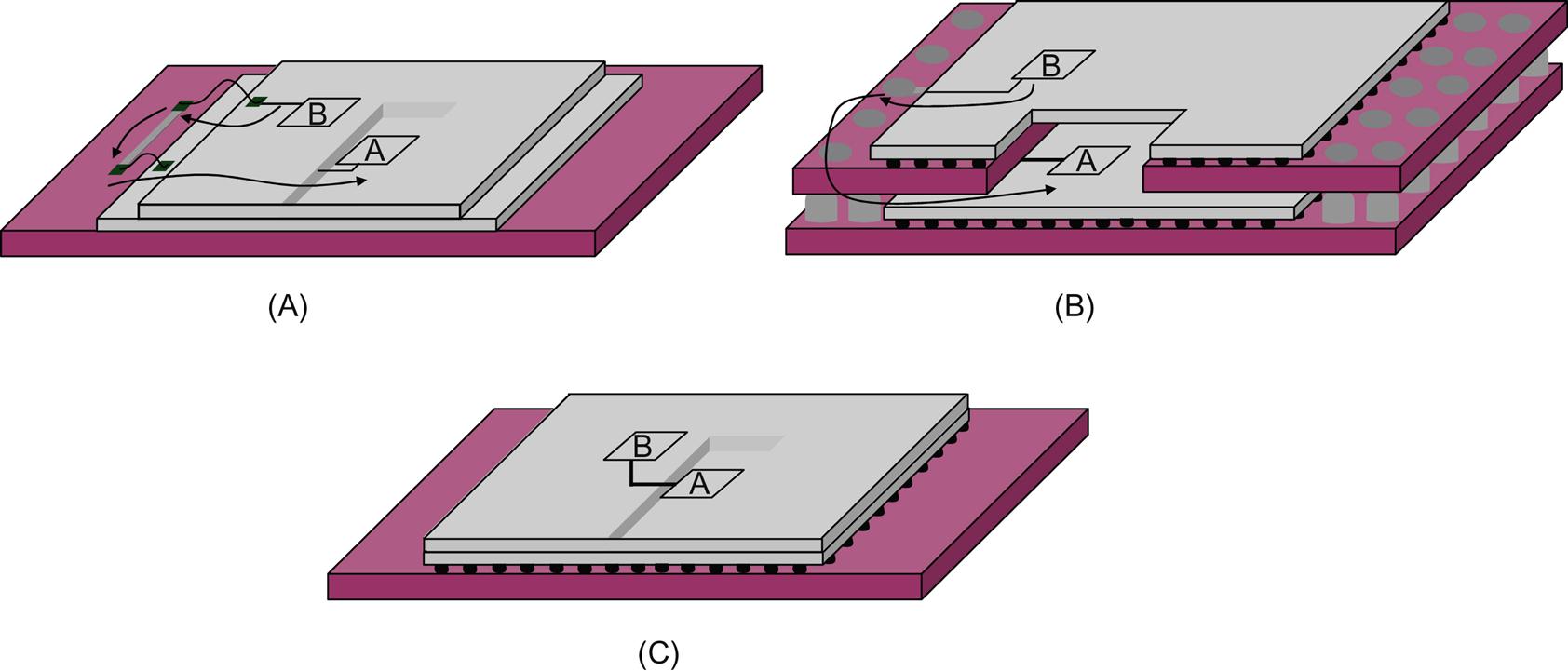
A system-in-package (SiP) offers a large number of advantages over traditional two-dimensional (2-D) system-on-chip (SoC), such as shorter off-chip interconnect lengths, increased packaging efficiency, and higher density. These advantages provide significant performance improvements as compared to a 2-D SoC. Manufacturing issues, however, limit the scaling of the interchip interconnects, such as the wire bonds and solder balls, within an SiP. Additionally, the inevitable increase in the delay of on-chip interconnects is not alleviated by SiP interconnect technologies. Although, an SiP employing coarse grain through silicon vias (TSVs) can improve this delay, the low density and impedance characteristics of these vertical interconnects limit the bandwidth of the intertier interconnect. The full potential of vertical integration is therefore not fully exploited. Consider, for instance, the SiPs depicted in Fig. 3.1, and assume that blocks A and B, located on different dies, are connected. The arrows, shown in Figs. 3.1A and B, represent typical interconnect paths connecting blocks A and B for each type of SiP. A 3-D IC, shown in Fig. 3.1C, provides the shortest interconnection between blocks A and B by utilizing a TSV. Consequently, 3-D ICs can achieve the greatest improvement in speed and power by decreasing the length of the long global interconnects as compared to other vertical integration technologies.
3-D ICs can be fabricated in either a batch (sequential) or parallel process. In the former case, the devices on the upper tiers of a 3-D stack are grown on top of the first tier, resulting in a purely monolithic system. Fabrication processes based on this type of 3-D circuit structure are discussed in Section 3.1. Alternatively, some ICs are prepared separately before the bonding process and bonded to form a 3-D system. Such a 3-D IC is a polylithic structure and related manufacturing processes are described in Section 3.2. Other techniques that provide contactless intertier communication have also been developed. Technologies for contactless 3-D ICs are reviewed in Section 3.3. One of the most important characteristics of polylithic 3-D ICs is the TSV, which provide an electrical connection among the circuits on different tiers, i.e., the intertier interconnects. Due to the significance of these vertical interconnects, Section 3.4 is dedicated to discussing the manufacturing process of the vertical vias and related issues. The technological implications of 3-D integration are summarized in Section 3.5.
3.1 Monolithic Three-Dimensional ICs
Monolithic or sequential 3-D ICs include stacking of circuits at the device level. Device level stacked 3-D ICs comprise layers of planar devices successively grown on a conventional CMOS or silicon-on-insulator (SOI) substrate. Several processes for monolithic devices were developed with moderate success in the 1980s; however, none of these processes reached high volume manufacturing primarily due to the decrease in manufacturing cost of transistors. However, as this cost has recently started to rise, interest in this technology has been revived. Past and more current efforts to manufacture high quality monolithic 3-D circuits are discussed in this section.
The first fabricated 3-D ICs were stacked bulk CMOS or SOI devices with simple logic circuitry. The devices comprising a logic gate can be located on different layers and, more importantly, manufactured with different technologies, such as CMOS or SOI. Independent of the technology utilized for the first device layer, these transistors are fabricated with conventional and mature processes. For the devices on the upper tiers, however, different fabrication methods are required. Several techniques, based on laser recrystallization or seed crystallization, are used to produce CMOS or SOI devices on the upper tiers and are described in Sections 3.1.1 and 3.1.2. The use of double-gate metal oxide semiconductor field effect transistors (MOSFETs) to form highly dense 3-D cells are discussed in Section 3.1.3. Recent methods on molecular bonding are presented in Section 3.1.4. Irrespective of the fabrication approach, the primary challenges for monolithic 3-D integration include fabrication of a high quality substrate for the upper layers, comparable performance of the devices in the bottommost layer with the performance of the FETs in the upper layers, and the use of low temperatures to manufacture FETs in these layers [96].
3.1.1 Laser Crystallization
Following the work in [97], several techniques using beam recrystallization were developed to successfully fabricate 3-D ICs. In these techniques, the first device layer is fabricated with a traditional CMOS or SOI process. Note that only a device layer is fabricated on the first tier. The interconnect layers are not fabricated at this initial stage. Fabrication of the transistors on the upper layers satisfies a twofold objective. The devices on the upper layers should exhibit satisfactory transistor electrical characteristics, such as field mobility, threshold voltages, and leakage currents (i.e., Ion/Ioff ratio) and the characteristics of the transistors on the lower layer should not be degraded by the high temperatures incurred during the manufacturing process.
The first layer of devices is formed with a common MOS process. Depending upon the fabrication process, this layer can include both PMOS and NMOS devices [98] or only one of the two devices [99]. In the latter case, the complementary type of devices is fabricated exclusively on the upper layer(s). Alternatively, the upper layer(s) can include only SOI devices [100].
Prior to the development of the upper device layer, an insulating layer of SiO2 is deposited [98]. To protect the devices of the first layer from the elevated temperatures during the recrystallization phase, a thick layer with an approximate thickness of 1 μm is deposited on top of the insulating SiO2 layer. This layer is a standard feature of the recrystallization technique and is composed of various materials, such as polysilicon [98], phosphosilicate glass [99], and silicon nitride (Si3N4).
To grow the devices on the upper layers, polysilicon islands or thin polysilicon films are crystallized to single grains by an Argon laser [101]. The resulting 3-D IC is shown in Fig. 3.2, where the different layers are also indicated. The temperature during the recrystallization phase can be as high as 950°C [100], while device formation with a lower temperature of approximately 600°C has been demonstrated [98].

Since the temperature used in these manufacturing steps approaches or exceeds the melting point of the metals commonly used for interconnects, doped semiconductor materials are used to interconnect the devices located on different tiers. These materials can include n+ doped polysilicon [98] or phosphorous-based polysilicon [100]. Alternatively, the interconnect layers can be fabricated after the upper layer devices are formed, where the contact holes are produced through reactive ion etching (RIE). The intertier interconnects are manufactured by sputtering aluminum [99]. A cross-section of a 3-D IC fabricated with aluminum interconnects is shown in Fig. 3.3.

The major drawbacks of the laser recrystallization technique are the quality of the grown devices on the upper layers and the effect of the high temperatures on the electrical characteristics of the devices on the lowest layer. Comparison of the device characteristics for the two layers shows that the threshold voltage is sufficiently controlled, while the mobility of the devices on the upper layer is slightly worse than the transistors on the bottom layer [99]. Since the mobility of the devices on the upper layers is degraded, the PMOS devices which exhibit lower mobility are fabricated on the lower layer [46]. In addition, simple shift registers [98] and ring oscillators [99] have been shown to operate correctly, demonstrating that the devices on the first layer remain stable despite the high temperature steps utilized to manufacture the devices on the upper layer.
More advanced recrystallization techniques can provide up to three device layers, where the lowest layer is a CMOS layer while the other two layers are composed of SOI devices [100]. Since there are three device layers in this structure, two isolation layers are required to protect the devices on the lower layers. Measurements from sample structures demonstrate that the threshold voltage of the devices is well controlled with low subthreshold currents for the devices on the upper layers [100]. The mobility of these transistors can, however, vary significantly.
Alternatively, E-beam has been used to recrystallize the polysilicon to form the devices on the upper layers [101]. A three-layer prototype 3-D IC performing simple image processing has been demonstrated [102]. On the topmost layer, consisting of amorphous-Si (a-Si), the light is captured and converted to a digital signal and stored on the bottom layer composed of the bulk-Si transistors. The intermediate layer, which includes the SOI transistors, compares the digital data from one pixel to the digital data in adjacent pixels to produce an edge detection operation. Measurements show a narrow distribution of the threshold voltage of the devices on the SOI layer with satisfactory I–V device characteristics. Although correct operation of the circuitry is confirmed, demonstrating the capabilities of a monolithic 3-D circuit, 34 mask steps are required, including five layers of polysilicon and two layers of aluminum interconnects. Although several recrystallization approaches have been developed, none of these techniques has demonstrated the capability of manufacturing complex, high performance 3-D circuits, primarily due to the inferior quality of the devices on the upper layers of the 3-D stack.
3.1.2 Seed Crystallization
Another technique to fabricate multiple device layers on bulk-Si is crystallizing a-Si into polysilicon grains. Thin film transistors (TFTs) are formed on these grains. The seed utilized for recrystallization can be a metal, such as nickel (Ni), or another semiconductor, such as germanium (Ge).
The basic processing steps of this technique are illustrated in Fig. 3.4. A film of amorphous silicon is deposited with low pressure chemical vapor deposition. A second film of low temperature oxide (LTO), SiO2, is deposited and patterned to form windows at the drain or both drain and source terminals of the devices for Ge or Ni seeding. Consequently, two kinds of TFTs are produced. One type is seeded only at one terminal while the second type is seeded at both terminals. The deposition of the LTO SiO2, patterning, and the deposition of the seed are additional steps as compared to a conventional process for TFTs. Thermal annealing is necessary to completely crystallize the channel films. Finally, the LTO and seeds are etched, permitting the TFTs to be fabricated with a standard process. A thermal layer of SiO2 is used as the gate dielectric, and boron and phosphorous doping is used for the junctions. The gate electrode is formed by in situ doped polysilicon and the interconnections are fabricated by modified interconnect and plug technologies from conventional 2-D circuits. The peak temperature of the process is 900°C.

Certain factors can degrade the quality of the fabricated TFTs, such as the size of the grains and the presence of defects within the channel region. Controlling the size and distribution of the grains contributes significantly to the quality of the manufactured devices. Comparisons among unseeded devices, produced by crystallizing a-Si, single seeded, and dual seeded TFTs, have shown that seeded devices exhibit enhanced device characteristics, such as higher field effect mobility and lower leakage currents. The greatest improvement in these characteristics is achieved by dual seeded TFTs. However, as compared to single seeded transistors, the improvements of dual seeded transistors diminish with device size. Consequently, for small devices where the grain size of a single seeded device is approximately the entire channel region, the performance of those TFTs is close to double seeded TFTs as grain boundaries are unlikely to appear within the channel. Grain sizes over 80 μm have been fabricated [104]. High performance TFTs formed by lateral crystallization on the upper layers exhibit low leakage currents and high mobility as compared to the SOI devices on the first layer, while significantly reducing the area of the logic gates [103,104].
Selective epitaxial growth (SEG) and epitaxial lateral overgrowth (ELO) have also been combined to fabricate multiple layers of SOI devices [105,106]. The various steps of these techniques are summarized in Fig. 3.5. The first device layer is formed on a thick layer of SiO2. The oxide is patterned with photolithography and etching procedures to define the SOI islands (Fig. 3.5A). A thinner SiO2 layer, acting as the insulator, is deposited (Fig. 3.5B). With photolithography, a window for SEG is opened within the silicon island patterns (Fig. 3.5C). Using SEG and ELO, the patterns are filled by vertical and lateral growth of silicon within the SEG window (Fig. 3.5D). The redundant silicon is etched with chemical mechanical planarization (CMP) (Fig. 3.5E). A second layer of devices is fabricated with the same process, unlike oxide deposition, which is achieved with plasma enhanced chemical vapor deposition. The transistors are fabricated on islands using conventional SOI techniques (see Figs. 3.5F to H). The smaller island has an area of 150 nm×150 nm, enabling a high degree of integration on a single die [105]. The photolithography and etching steps limit the dimensions of the SOI islands. Satisfactory device characteristics have been reported with stacking faults only appearing on the first device layer [105].

3.1.3 Double-Gate Metal Oxide Semiconductor Field Effect Transistors for Stacked Three-Dimensional ICs
Similar to 2-D circuits where standard cell libraries include a compact physical layout of individual logic gates or more complex logic circuits, standard cell libraries for 3-D circuits include “volumetric” logic cells with minimum volume and a smaller load as compared to 2-D cells. Fabrication techniques that use local clusters of devices to form standard 3-D cells have been developed [107] based on double-gate MOSFETS [108,109]. The major fabrication stages for a 3-D inverter cell are illustrated in Fig. 3.6, where a decrease of 45% in the total capacitance is achieved. Similar improvements are demonstrated for more complex circuits, such as a 128-bit adder, where a 42% area reduction is observed [107].

An SOI wafer is used as the first layer of the 3-D IC. The top silicon layer is thinned by thermal oxidation and oxide etching. A thin layer of oxide and a layer of nitride are deposited as shown in Fig. 3.6A. The wafer is patterned and shallow trench etching is used to define the active area (Fig. 3.6B). A layer of LTO is deposited to fill the trench, which is planarized with CMP, where the nitride behaves as the stop layer (Fig. 3.6C). The nitride film is removed and LTO is utilized as a dummy gate. The LTO, silicon, and oxide are patterned and etched, followed by depositing a nitride film (Fig. 3.6D). The drain and source regions for the first device layer are created with an As+ implantation. As depicted in Fig. 3.6E, a via is opened at the drain side to connect the terminals of the NMOS and PMOS transistors located on the second layer. The contact is implemented as a tunneling ohmic contact. A polysilicon layer is deposited and planarized by CMP utilizing the nitride film as the stop layer. The nitride film is etched to expose the silicon for the channel region (Fig. 3.6F). Boron doping is used to fabricate the source and drain regions of the PMOS transistor on the top layer (Fig. 3.6G). The active area for the devices is defined by removing the LTO and the buried oxide (Fig. 3.6H). Before forming the gates for the stacked transistors, the gate oxide is grown by thermal oxidation, as shown in Fig. 3.6I. Finally, in situ deposition of doped polysilicon forms the gate electrodes. Note that for the gate below the channel region of the PMOS transistor (see Fig. 3.6J), a slow deposition rate is required to completely fill this region.
3.1.4 Molecular Bonding
Monolithic 3-D circuits utilizing molecular bonding demonstrate several advantages over the previously described approaches. An important trait of this technique is that an entire wafer can be transferred onto the bottom layer at low temperature (200°C), where the transistors for the upper layers are formed. There are several advantages associated with this approach, for example, the quality of the substrate, which is not limited by defects as in the case of seed crystallization and recrystallization-based methods. Furthermore, the integration density is the same as the bottommost layer, whereas the seed windows and the polycrystalline nature of the substrate in other approaches limit this density. Additional benefits of a high quality monocrystalline substrate are better bonding and improved control of the substrate thickness [110].
Although this technique includes the transfer of the substrate onto another wafer, resembling the case of 3-D integration with TSVs, the devices on the upper layers are not yet fabricated, which greatly differentiates the manufacturing process. The manufacturing process includes a number of sequential steps, which commences with the fabrication of the devices in the bottom layer with standard fully depleted silicon on insulator (FDSOI) processes. These steps are summarized in Fig. 3.7. A thin layer of dielectric is deposited and planarized before the transfer of the substrate. The thickness of the dielectric layer is an important factor, which can be adapted to exploit the coupling between the stacked devices [111], where thicknesses ranging from 60 nm to 110 nm have been tested. In the next step, molecular bonding is used to transfer an SOI substrate (see Fig. 3.7B) (other substrates can also be transferred, which makes this technology appealing).

Having a high quality substrate, the devices are formed where the orientation of these devices can be controlled to achieve specific transistor characteristics [110,111]. Furthermore, non-Si devices, such as Ge p-MOSFETs [112] and devices other than bulk MOSFETs, can be grown, including FinFETs and trigate transistors [113,114] (see Fig. 3.7C). One critical step for the performance of the transistors in the upper layers is activation of the dopants, which for the bottom layer is achieved with high temperatures (e.g., >1000°C) [96]. These temperatures, however, are prohibitive for thermal activation of the dopants in the upper layer(s). Consequently, solid phase epitaxy regrowth is applied at 600°C irrespective of the type (n or p) of the transistor. The last major step of the process includes the interlayer interconnects, which are similar to standard contacts used in the BEOL of planar circuits (see Fig. 3.7D). Case studies with tungsten contact plugs have been demonstrated [96]. The similarity of an interlayer contact with a typical contact between two metal layers is illustrated in Fig. 3.8.

Since different types of devices can be manufactured, several applications can be supported by monolithic 3-D circuits. This situation is also due to monolithic 3-D technology able to support integration at both the device and cell level. Thus, the integration of different device types leads to heterogeneous applications, while integration at the cell level leads to considerable gains in performance and area for the logic and memory circuits. The disparate applications enabled by this technology are listed in Table 3.1.
Table 3.1
Potential Applications for Monolithic Integration at the Device Level [110]
| Application | Layer | Example of Partitioning | Best Suited Technology |
| Field programable gate array (FPGA) | 1 | Pass gate | High performance transistors |
| 2 | 6T SRAM | Low standby power transistors | |
| Highly miniaturized pixels | 1 | Photodiode and transfer gate | 1 μm thick SOI with backside illumination |
| 2 | Readout transistors | Low noise transistors with relaxed (L, W) and gate oxide | |
| CMOS gates | 1 | nFET | nFET gate stack, tensile-Si or InGaAs |
| 2 | pFET | pFET gate stack, compressive-Si or Ge or (110) Si |

Integrating monolithic circuits at the device level allows for adapting the behavior of the devices in several ways. For example, the choice of substrate, the material used for the channel, the orientation of the crystal, and the strain can each be used to produce devices that are best adapted for the target application [96]. An example of this approach is 4T SRAM (loadless) cells, where the transistors are vertically aligned to ensure that the stored bit of information back biases the access transistors (grown in the upper layer), shifting the threshold voltage of these transistors [115]. The transistors should be carefully aligned to modulate the threshold voltage of the devices in the upper layer based on the applied gate voltage to the devices in the lower layer. Furthermore, the thickness of the interlayer dielectric (ILD) separating the two layers of transistors should be appropriately adapted. Simulations have shown that if this thickness is 300 nm, no noticeable change in the threshold voltage is observed due to the gate voltage of the transistors in the bottom layer. If this thickness decreases to 10 nm, the shift in voltage threshold can be as high as 130 mV [115].
The benefit of this approach is improved stability of the memory cell. The read noise and static noise margins are, respectively, 320 and 150 mV [115]. Additionally, the noise margins are achieved without any modification to the size of the devices. Both the transistor width and length are, therefore, the same for all four of the transistors in the SRAM cell.
Although transistor level integration is beneficial in this specific example, significant and higher gains are demonstrated when integration occurs at the cell level. In this approach, cells are placed on top of other cells, yielding more compact circuits. To compare the gains produced from each integration technique, the area savings and performance improvements are evaluated for some basic logic gates and circuits. A flip flop in these two styles exhibits a density gain of 28.5% and 38% for integrating, respectively, nFETs on top of pFETs and CMOS gate-on-gate integration. For more complex circuits, such as a 16-bit multiply accumulate unit, the savings are, respectively, 42% and 52% for the two integration styles [112]. Alternatively, if the area is maintained constant, increased performance can be achieved. Thus, for a NAND gate with a driving strength of 8×, the gain in current is 20% and 100%, respectively, when integrating at the transistor and cell level.
These examples demonstrate that integration at the cell level offers considerable improvements. Application of this integration style has also been applied to FPGA fabrics, where the fabric is partitioned to ensure that the memory cells are placed on the bottom layer whereas the logic cells are placed on the upper layer. The savings in area and energy delay product are, respectively, 55% and 47%.
Although monolithic integration exhibits appealing characteristics, integrating several layers of devices with a single stack of interconnect layers (i.e., BEOL) is a challenging task. Alternatively, fabricating a 3-D system with vertically bonded ICs or wafers that are individually processed can reduce the total manufacturing time without sacrificing the quality of the devices on the upper tiers of the stack. Consequently, parallel or polylithic integration, through where circuits from individual wafers are stacked to form multi-tier systems, is discussed in the following sections.
3.2 Three-Dimensional ICs with Through Silicon Via or Intertier Via
Wafer or die level 3-D integration techniques, which utilize TSVs, are appealing candidates for 3-D circuits. Intertier vias offer the greatest possible reduction in wirelength with vertical integration. In addition, each tier of a 3-D system can be processed separately, decreasing the overall manufacturing time. As each tier of the 3-D stack is fabricated individually, a high yield process can be utilized for each tier suitably tailored to the nature of the circuit in that tier, e.g., memory or logic. A broad spectrum of fabrication techniques for 3-D ICs has been developed. These techniques support either wafer or die level 3-D stacking and are discussed, respectively, in Sections 3.2.1 and 3.2.2. The different bonding approaches and related issues are discussed in Section 3.2.3.
3.2.1 Wafer Level Integration
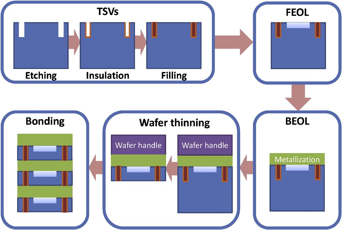
Although none of the developed wafer level techniques has been standardized, nearly all of these methods share similar fabrication stages, which are illustrated in Fig. 3.9. The order of these stages, however, may not be the same or some stages may not be used, depending upon the TSV fabrication scheme and the bonding approach and mechanism.

Initially, CMOS or SOI wafers are separately processed to produce the physical tiers of the 3-D stack, while a certain amount of active area is reserved for the TSVs. The TSVs are etched and filled with metal, such as tungsten (W) or copper (Cu), or even low resistance polysilicon. To decrease the length of the TSVs, the wafers are attached to an auxiliary wafer, usually called a “handle” or “carrier” wafer, and thinned to a different thickness depending upon the target aspect ratio for the TSVs. After the TSVs are revealed, backside metallization provides electrical connections between the tiers. The alignment and bonding phase follows, as shown in Fig. 3.9D. Finally, the handle wafer is removed from the thinned wafer and, if required, the appropriate side of the wafer is processed and attached to another tier. A broad gamut of materials and methods exist for each of these phases, some of which are listed in Table 3.2.
Table 3.2
Characteristics of Fabrication Techniques for 3-D ICs
| Process From | IC Technology | Intertier Vias Material | Wafer Thinning Thickness | Alignment Accuracy (μm) | Tier Bonding Material | Bumps | Handle Wafer |
| [116,117] | SOI | W | 500 nm | ±3 | Cu–Cu pads | Yes | Yes |
| [118,119] | SOI | Cu | ~10 μm | 1–2 | Polymers | No | No |
| [120] | SOI/CMOS | W | ~10 μm | N/A | Cu/Sn | Yes | Yes |
| [121] | CMOS | Cu | <2 | Polymer | No | Yes | |
| [122] | SOI/CMOS | n+ poly – Si/W | 7–35 μm | ±1 | Epoxy adhesive | Yes | Yes |
| [123] | SOI | Cu | ~ 2 μm | <1 | Oxide fusion | No | Yes |

Several of the proposed techniques for 3-D ICs support the integration of both CMOS and SOI circuits [120,122]. From a fabrication point of view, however, SOI facilitates the wafer thinning step as the buried oxide (BOX) serves as a natural etching stop layer. This situation is due to the high selectivity of the etching solutions. Solutions with a Si to SiO2 selectivity of 300:1 are possible [116]. In addition, SOI technology can yield particularly thin wafers or tiers (<10 μm), resulting in short TSVs. Alternatively, SOI circuits inherently suffer from poor thermal properties due to the low thermal conductivity of the oxide [124].
The formation of the TSVs is an important issue in the design of high performance 3-D ICs. This fabrication stage includes opening deep trenches through the silicon substrate (and potentially the inter layer dielectric and metal layers), passivation of the trench sidewalls from the conductive substrate (for CMOS circuits), and (partially or fully) filling the opening with a conductive material to electrically connect the tiers of the 3-D system. Due to the importance of this fabrication stage a more complete discussion of TSVs follows in Section 3.4.
Before stacking the tier, the wafers are thinned to decrease the overall height of the 3-D system and, therefore, the length of the TSVs. The diameter and length of the TSVs are interdependent and are typically characterized by the TSV aspect ratio (length/diameter). Processes that produce TSVs with aspect ratios over 20:1 [125] have been demonstrated. Typical ratios range from six to ten [126,127], where six is a common ratio. Furthermore, the minimum diameter of the TSVs depends upon the preferred integration granularity in addition to the capabilities of the manufacturing processes. In general, the finer the level of integration, the more aggressive the TSV aspect ratio or wafer thinning process.
A reduced wafer thickness, however, cannot sustain the mechanical stresses incurred during the handling and bonding phases of the 3-D process. A handle wafer is therefore attached to the original wafer prior to the thinning step. The handle wafer should possess several properties including the following:
• Mechanical durability to withstand the mechanical stresses incurred during the wafer thinning process due to grinding and polishing, and during bonding, due to compressive and thermal forces.
• Thermal endurance to processing temperatures during wafer bonding and bumping.
• Chemically inert to the solutions employed for wafer thinning and polishing.
• Simple and fast removal of the thinned wafer with appropriate solvents.
• Precise wafer alignment; for example, by being transparent to light.
Thinning can proceed with a variety of methods, such as grinding and etching or both, accompanied by polishing. Various combinations can also be applied, such as a silicon wet etch followed by CMP, mechanical grinding with CMP, mechanical grinding succeeded by a spin etch, and dry chemical etching [119]. Several requirements relating to the wafer thinning step also exist, including [128]:
• Few defects and damage during thinning
• Few defects and damage during edge trimming
• Careful control of the thinning process to ensure uniform wafer thinning until the desired thickness is achieved. The total thickness variation (TTV) should remain low at the target thickness.
Accurate alignment of the thinned wafers is a challenging task. A variety of techniques are utilized to align the wafer based on the precise registration of the alignment marks. These mechanisms include infrared alignment, through wafer via holes, transparent substrates, wafer backside alignment, and inter-substrate alignment [129]. Typical alignment precisions range from 1 to 5 μm (see Table 3.2). Submicrometer accuracies have also been reported [123,129].
Once the wafers are aligned, the bonding step follows. Disparate methods to perform this step are listed in Table 3.3. If die-to-wafer or die-to-die bonding is preferred to avoid the integration of faulty dies, each wafer is diced prior to bonding and the dies are successively bonded. An increase in the turnaround time, however, is inevitable with this approach as discussed in the following subsection.
Table 3.3
Comparison of Bonding Technologies [130]
| Bonding Type | Metal Bonding | SiO2 Bonding | Hybrid Bonding (Metal and Adhesive) | ||
| C4 Bonding | Intermetallic Compound Bonding | Cu–Cu Bonding | |||
| Bonding temperature | ~260°C | ~260°C | ~400°C | Room temp. | ~300°C |
| Heat tolerance | <260°C | <450°C* | <1084°C | <1400°C | <400°C* |
| Connectivity | Mechanical and electrical | Mechanical and electrical | Mechanical and electrical | Mechanical | Mechanical and electrical |
| Interconnection pitch | Low | Middle | Middle | High | Middle |
| Chip level applicability | High | High | Medium* | NA | Medium* |
| Wafer level applicability | Low | Medium* | Medium* | High | Medium* |
| Issues | Low heat tolerance, large I/O pitch | Intermetallic compound (IMC) thickness control, reliability | Thermal and compression stress, flatness, cleaning | Flatness, voids/particles | High bonding pressure, processing, integrity, flatness |

*The applicability can vary depending upon the detailed steps of the process and the requirements of the aimed application.
3.2.2 Die-to-Die Integration
With die-to-die 3-D stacking, the wafer is diced and each die is separately tested. The known good dies are placed on supporting wafers and these carrier wafers are bonded, producing a two-tier system. This approach has a better manufacturing throughput than individual die-to-die bonding but a lower throughput than direct wafer level bonding where some of the dies can be defective.
Another approach to allow multiple die-to-die stacking rather than only two-tier systems is the cavity alignment method where multiple tiers are assembled, improving manufacturing throughput. The method utilizes a silicon substrate with metal layers, which provides mechanical support for the entire stack. A template that forms the cavity is deposited with the use of an optical microscope to obtain precise placement of the template. The template is composed of a metal plate with a thickness of 0.5 mm and exhibits a small coefficient of thermal expansion (CTE). Upon alignment, the template is bonded to the substrate with a removable adhesive [130]. The tiers of the system are placed sequentially into the cavity where bonding is achieved by compression. A final bonding step is applied to the entire system based on thermal compression, where a typical applied temperature is 250°C and the exerted force is 10 N. The process is completed by removing the template. The stages of the process are illustrated in Fig. 3.10. The alignment accuracy of this method is within ±1 μm.

Other die-to-die integration techniques that can produce up to four-tier systems have also been demonstrated, which, although based on conventional bonding through thermal compression, utilize scrubbing and heating to enhance bonding strength [131]. In this process, the first die is of regular thickness, while the upper tiers are thinned to 50 μm. Scrubbing improves the TTV of the bump height of the TSV, and the surface flatness of the copper bumps. With the introduction of a scrubbing force the bonding temperature can be lowered to less than 200°C, while the pressure is also decreased to less than 100 MPa. Key parameters of this technique are the scrubbing time and force [131]. Tests on daisy chain connections of TSVs bonded with this approach demonstrate a resistance of approximately 170 mΩ, close to the theoretically expected resistance of 113 mΩ [131].
Alternatively, wafer scale bonding exhibits the highest manufacturing throughput. Wafer level bonding can be applied with a high initial yield for each tier within a 3-D system (the overall yield can be affected by later processing steps, e.g., bonding). Thus, wafer scale stacking results in an acceptable overall yield for the 3-D system, assuming the yield for each tier is high.
3.2.3 Bonding of Three-Dimensional ICs
In addition to the level of bonding, different bonding styles also exist. For example, back-to-face tier bonding is illustrated in Fig. 3.9D. In addition, face-to-face bonding can be utilized to efficiently bond two tiers. An advantage of face-to-face bonding is that if only two tiers are bonded, the TSVs can be removed, as shown by the process illustrated in Fig. 3.11. In this process, the “mother” circuit is considerably larger and provides the interconnections to the package. For this reason, two different types of bumps are utilized. Microbumps with a fine pitch (25 to 35 μm) connect the two tiers, while Cu pillars at a 185 μm pitch interconnect the two tier system to the package. Adding, however, a third tier to a two tier stack is not straightforward since TSVs are required. In this case, the third (or other) tier is added in a back-to-face manner, which requires TSVs. Back-to-back bonding is also possible, resulting, however, in longer and, therefore, lower performance TSVs.

Bonding can be achieved with adhesive materials, metal-to-metal bonds, oxide fusion, and eutectic alloys deposited among the tiers of a 3-D system [117]. A list of the traits and challenges of these disparate bonding technologies are reported in Table 3.3. Epoxies and polymers possess good adhesive properties and are widely used. Some of these polymers are listed in Table 3.4. Metal-to-metal bonding requires the growth of (square) bumps on both candidate tiers for stacking and can consist of, for example, Cu, Cu/Ta, In/Au, and Cu/Sn. A portion of these bumps is deposited at the edge of the TSVs, providing enhanced electrical connection between the tiers. In the case where metals with different melting points are utilized (for example, Cu and Sn), the metal with the lower melting point is placed between the Cu pillars with the higher melting point [130]. An inter-metallic compound (IMC) is formed by applying thermal compression to ensure that the metal with the lower melting point diffuses into the metal with a higher melting point.
An epoxy filler can also be used to reinforce the bonding structure. An issue that arises in this case, however, is that the resin can result in bonding failure due to differences in the height of the metal bumps. To avoid these failures, pyramid or conic shaped bumps have been proposed [133]. The compressive bonding force causes the bumps to spread, excluding the resin from the bond region, as illustrated in Fig. 3.12. Eutectic solders are also used for tier bonding, where tin is plated on the tier surface followed by heating and compression [120]. Additionally, the temperature profile depends upon the material used for the interface and typically ranges from 200 to 400°C to not degrade the copper interconnections. Other highly refractory metals, such as tungsten or doped polysilicon, can be used if higher temperatures are necessary, increasing, however, the resistance of the TSVs.

Oxide fusion is another typical technique for bonding, where bonding films are used for this purpose. The advantages of oxide bonding include avoidance of high stresses due to the thermal compression, higher tolerance to the alignment accuracy thereby enhancing reliability, and the suitability of this approach for dense and fine pitch TSVs [128,134]. Alternatively, issues with oxide bonding primarily relate to the bonding films, where key requirements include [128,130]
• Careful control of the film composition;
• Smooth surface of the oxide bonding films at the atomic level to strengthen the bonding density and limit the presence of nanovoids at the bonding interface;
• Clean surface of the bonding films to avoid microvoids due to the presence of particles from foreign materials and process residues.
Depending upon the bonding mechanism and material, certain requirements should be satisfied to avoid delamination and cracking of the tiers:
• Small mismatch between the CTE of the bonding material and the tiers
• Mechanical endurance in the later processing steps
• No outgassing of the adhesives from heating, which can result in void formation
• No void generation due to the presence of residues on the layer surfaces
Achieving a reliable bond throughout the lifetime of a 3-D stack is an important requirement for any bonding and/or assembly process. A host of tests based on industry standards are applied to ensure the reliability of the manufactured 3-D stack [140]. These reliability tests include [130,141]:
• Temperature cycling (e.g., −40 to 125°C)
• High temperature storage (for example, at 150°C)
• Humidity test (e.g., 85°C at 85% RH)
• Pressure cooker test (e.g., 121°C at 100% RH)
• Unbiased highly accelerated stress test (e.g., 130°C, 85% RH)
• Razor tests, where a razor blade is used to penetrate the interface between the tiers, while other tests can include bending forces applied to the bonded wafers [118].
The final processing step for a 3-D IC with TSVs is removal of the handle wafer and cleaning the tier surface if subsequent bonding is required. A variety of solutions can be used to detach the handle wafer. The time to accomplish this step also depends upon the size of the wafer [120].
3.3 Contactless Three-Dimensional ICs
Although the majority of the processes developed for 3-D ICs utilize vertical interconnects with some conductive material, other techniques provide communication among circuits located on different tiers through coupling of electric or magnetic fields. Capacitively coupled circuits are presented in Section 3.3.1. Inductive vertical interconnects are discussed in Section 3.3.2.
3.3.1 Capacitively Coupled Three-Dimensional ICs
In capacitively coupled signaling, the TSVs are replaced with small on-chip parallel plate capacitors that provide intertier communication to the upper tier. A schematic of a capacitively coupled 3-D system is illustrated in Fig. 3.13 [142]. A buffer drives the capacitor. The receiver circuitry, however, is more complex, as the receiver must amplify the low voltage signal to produce a full swing output. In addition, the receiver circuit should be sufficiently sensitive and fast to detect and respond to the voltage transferred through the coupling capacitors. The maximum voltage level that can be propagated through a coupling capacitance Cc is [143]
(3.1)
where Cp is the capacitance of the capacitor plate to the substrate and adjacent interconnect preceding the receiver. The denominator in (3.1) includes the capacitance of the transistors at the input of the receiver.

A 5 fF capacitance has been used in [143] to transmit a signal to several receiver architectures. This capacitance uses 20 μm×20 μm electrodes with a separation of 2.5 μm (e.g., dielectric thickness) and a dielectric constant of 3.5. Simulations indicate correct operation for frequencies up to 500 MHz, while measurements show successful operation for signal transmission up to 25 MHz for a 0.5 μm CMOS technology. Smaller parallel plate capacitor structures and improved transceiver circuitry have also been reported, yielding a communication bandwidth of 1.23 Gb/s [144]. For a 0.13 μm CMOS technology the size of the capacitor electrodes is 8 μm×8 μm. Comparing capacitively coupled 3-D ICs with SiP, where the intertier wiring is over the edge of the IC (the total interconnect length is on the order of a centimeter), a 30% improvement in delay is demonstrated. In addition, significant dynamic power is saved with this interconnect scheme. The static power consumed by the receiving circuitry, however, decreases the overall power savings.
The parasitic capacitance of the devices is greatly reduced with a silicon-on-sapphire technology, an early type of SOI technology [142]. This situation is particularly advantageous for power transfer circuits realized with a charge pump. The transceivers and charge pump circuits have been fabricated in a 0.5 μm CMOS technology [142], utilizing capacitors with dimensions of 90 μm×90 μm. The distance between the two tiers is 10 μm. Decreasing the separation between the tiers can increase the coupling, requiring smaller capacitor plates to propagate a signal. The capacitors used for the power exchange should be large, though, for enhanced coupling. A prototype based on this technique provides approximately 0.1 mA current to the devices on the upper tiers. Successful operation up to 15 MHz has been demonstrated [142].
Critical factors affecting this technique are the size of the capacitors, which affects the interconnect density, the intertier distance, and the dielectric constant of the material between the tiers, which determine the amount of coupling. Face-to-face bonding is preferable as the distance between the tiers is shortened. Interconnecting a 3-D IC consisting of more than two tiers with this approach, however, is a challenging task.
3.3.2 Inductively Coupled Three-Dimensional ICs
Inductive coupling can be an alternative for contactless communication in 3-D ICs. Each tier in a two-tier 3-D IC accommodates a spiral inductor, located at the same horizontal coordinates (see Fig. 3.14). The size and diameter of the inductors are based on an on-chip differential transformer structure [145]. Inductors with a diameter of 100 μm have been shown to be suitable for signal transmission, where the inductors are separated by a distance of 20 μm. In contrast to capacitively coupled 3-D ICs, signal propagation is achieved through current pulses. As compared to the capacitive coupling technique, specialized circuitry both for the transmitter and receiver is required, dissipating greater power. A current-mode driver generates a differential signal. The receiver amplifies the transmitted current or voltage pulses, producing a full swing signal. Alternatively, inductive coupling does not require as small a separation of the tiers as with the capacitive coupling technique, relaxing the demand for thin spacing between tiers. This advantage supports the integration of more than two tiers for inductively coupled 3-D ICs. Simulations indicate 5 Gb/s throughput with 70 ps jitter at the output, consuming approximately 15 mW [145].

The main limitations of this technique include the size of the inductors, which yields a low interconnect density as compared to the size of the TSVs, increased power consumption of the transceiver circuitry, and interference among adjacent on-chip inductors. Additionally, power delivery to the upper tiers is realized with galvanic connections for high performance applications. Consequently, the fabrication process and cost for this type of 3-D IC is not greatly simplified as the TSV formation step is not eliminated for this type of applications. Alternatively, applications that lie in the low power regime can benefit more from this approach by eliminating the galvanic connections between tiers and supporting contactless power transfer in addition to wireless signaling. Due to the potential of this contactless scheme, Chapter 6, Three-Dimensional ICs with Inductive Links, is dedicated to the design and modeling of inductive links for contactless 3-D systems.
3.4 Vertical Interconnects for Three-Dimensional ICs
Increasing the number of tiers that can be integrated into a single 3-D system is a primary objective of three-dimensional integration. A 3-D system with high density vertical interconnects is therefore indispensable. Vertical interconnects implemented as TSVs produce the highest interconnect bandwidth within a 3-D system as compared to wire bonding, peripheral vertical interconnects, and solder ball arrays. Other important criteria should also be satisfied by the fabrication process for TSVs. A fabrication process for vertical interconnects should produce reliable and inexpensive TSVs. In addition, a TSV should exhibit low impedance characteristics. A high TSV aspect ratio, the ratio of the length of the via to the diameter of the top edge, may also be required for certain types of 3-D circuits. The effect of forming the TSVs on the performance and reliability of the neighboring active devices should also be negligible.
As shown in Fig. 3.9, TSVs are formed after both the active devices (i.e., front end of line (FEOL)) and the metal layers (i.e., BEOL) on each tier of the 3-D circuit are fabricated. In this case, the TSV fabrication process is called a “via-last” approach, as also shown in Fig. 3.15. In via-last processes, the TSVs typically have large aspect ratios. TSV formation for via-last processes is a complicated step as etching is performed through several materials, such as metal and dielectric, in addition to the silicon substrate. Another approach, as depicted in Fig. 3.16, commences the fabrication of a 3-D system with the formation of TSVs. In this case, since neither the FEOL nor the BEOL are fabricated, the TSV process is called a “via-first” approach. Via-first approaches usually have faster etching rates, as only the silicon substrate is etched, and support smaller aspect ratios. However, as the FEOL requires high temperatures, care should be placed to maintain the reliability of the TSVs and control the stresses developed during the thermal cycles required by the FEOL.

A TSV manufacturing approach that encounters fewer thermal and reliability challenges is the case where TSVs are formed after the FEOL but before the BEOL. This approach is called “via-middle” and is shown in Fig. 3.17. In this case, the formed TSVs maintain a low aspect ratio as compared to via-last processes without undergoing the high temperatures due to the FEOL in via-first approaches. Some TSV processes with information about the physical and electrical traits of the TSVs are reported in Table 3.5.

Table 3.5
Dimensions and Electrical Characteristics of the TSVs
| Process From | Depth (μm) | Diameter (μm) | Total Resistance (mΩ) |
| [121] | 25 | 4 | 140 |
| [146] | 30 | 2×12 | 230 |
| [147] | 80 | 5 and 15 | 9.4 or 2.6 |
| [147] | 150 | 5 and 15 | 2.7 or 1.9 |
| [148] | 90 | 75 | 2.4 |

The TSVs can be formed as blind vias exposed during the wafer thinning step. This method provides the important advantages of compatibility with existent process flows and simplicity in wafer handling [149]. A disadvantage of this approach is the effect on reliability resulting from wafer thinning and bonding. Alternatively, the TSVs can be fabricated after the wafer thinning step [150–152], as depicted in Fig. 3.18. This approach alleviates those problems related to back end processing; however, this method requires several processing steps with thin wafer handling, a potential source of manufacturing defects. Despite the disadvantages of the via-first approach, via-first, and via-middle approaches currently appear as the most promising technologies for TSVs.

The manufacturing technology for TSVs was greatly advanced by the invention of the BOSCH process in the mid-1990s, which was initially used to fabricate micro-electro-mechanical systems [153]. The BOSCH process consists of two functions, namely, etching and deposition, applied in successive time intervals of different duration (typically on the order of seconds) [149,154,155]. Sulphurhexafluoride (SF6) is utilized for the etching cycles, while fluorocarbon (C4F8) is used to passivate the lateral walls of the TSV [153–155]. The BOSCH process is followed first by depositing a barrier, after which a seed layer is deposited. The former layer, typically consisting of TiN or TaN deposition, prevents the Cu from diffusing into the silicon as in a conventional damascene process. The latter layer is utilized for the filling step of the TSV. Copper is mostly used for via filling.
Although tungsten or low resistance poly-Si can be used for the TSV, copper has the inherent advantage of compatibility with BEOL processing and the multilayer interconnects used in modern ICs. Copper, however, may not be the appropriate material for via-first processes, as the FEOL requires high temperatures that can exceed the melting point of the copper. Although the BOSCH process is effective in etching silicon, several issues regarding the quality of the TSVs have to be considered [149], such as
• Controllability of the via shape and tapering;
• Conformal deposition and adhesion of the insulation, barrier, and seed layers;
• Void free filling with a conductive material;
• Removal of excessive metal deposition along the edges of the TSV.
TSVs have either a straight or tapered shape with different aspect ratios, as illustrated in Fig. 3.19. The aspect ratio (i.e., D/W) ultimately depends upon the thickness of the wafer that results from the wafer thinning step, where this ratio can exceed 20 [125]. Typical aspect ratios, however, are below ten. TSVs with a wide range of diameters have also been manufactured [147,149,150,153]. Tapered vias are preferred to nontapered vias, as a lateral wall with a slope and smooth surface facilitates the deposition of the barrier and seed layers and the following fill step [149]. This behavior occurs because the tapered profile decreases the effective aspect ratio of the straight segment of the TSV. Excessive tapering, however, can be problematic, leading to V-shaped vias at the bottom edge. In addition, a specific interconnect pitch is required at the bottom side of the via; consequently, tapering should be carefully controlled.

Although the BOSCH process can etch silicon sufficiently fast, producing a smooth surface, barrier, and seed layer deposition is not a straightforward task. The BOSCH process results in a particularly rough surface, producing scallops, as illustrated in Fig. 3.20 [156]. Note that the roughness of the surface decreases with the via depth. The rough sidewall is due to the time multiplexed cycles of the etching and deposition steps of the BOSCH process. A low surface roughness is of particular importance for the steps that follow the via formation process. The scallops not only prevent a conformal barrier and seed layer deposition but also increase the diffusion of the copper into the silicon despite the presence of the barrier layer [157].

Different thermal loads can result from the following processing steps, such as wafer bonding, where thermal compression is typically utilized. Finite element analysis of TSVs with a diameter ranging from 3 to 10 μm has demonstrated that thermal loads contribute more to the induced stresses on a TSV as compared to those stresses caused by the bonding force. For specific bonding conditions, where the applied bonding force is 300 N and the temperature ranges from 300 to 400°C, the thermal loads constitute 84% of the total induced stress [158]. Simulation of the thermal loads imposed on the TSVs indicates that the thermal stress, due to the CTE mismatch between the dielectric and the metal filling, is more pronounced at the region where the scallops are sharper [156]. These stresses can crack the dielectric layer, increase the current leaking into the silicon substrate, or cause delamination of the copper within the TSV.
Another problem related to deep RIE concerns the silicon undercut below the mask at the upper and wide edge of the TSV. Uncontrolled undercut can lead to mask overhang, which can accelerate plating at the top of the TSV. Faster plating of the upper edge of the via can lead to premature closing of the via and to formation of a void inside the TSV [154].
Two key parameters can be used to adjust the surface roughness of the TSV sidewalls: the ratio of the time duration of the etching and passivation steps and the flow of the C4F8 [155]. In addition, variations of the BOSCH process or two step processes can be used to adjust the roughness of the TSV surface. For example, manufacturing process parameters, such as the pressure, bias power, and etching cycle time, can be varied in time rather than maintained static throughout the etching step. With this approach, the roughness of the surface has been decreased from ~0.05 to ~0.01 μm [156].
Via formation is followed by deposition of the barrier and seed layers. The primary goal of this step is to achieve a conformal profile throughout the depth of the TSV, which is increasingly difficult for TSVs with high aspect ratios. Different chemical vapor depositions are typically utilized for this step to provide good uniformity with moderate processing temperatures. Metal organic chemical vapor deposition (MOCVD) can be utilized to deposit the barrier layer. The disadvantage of this method is poor adhesion. In addition, MOCVD or atomic layer deposition used mainly for TSV with high aspect ratios are slow and expensive processes. Alternatively, physical vapor deposition (PVD) can be applied for layer deposition, which yields fair adhesion at low temperature. PVD, however, results in poor uniformity.
Via filling is achieved by electroplating, where the copper filling is grown laterally on the deposited seed layer. Alternatively, electroplating can be applied in a bottom-up manner, where a contact wafer is attached to the bottom of the device wafer, which includes the via openings. A major issue of this technique is the difficulty in removing the contact wafer, which provides the seed layer for the via filling [155]. Copper electroplating should produce uniform and void free TSVs to achieve high quality signal paths. Poor electroplating conditions that result in void formation within the TSV are illustrated in Fig. 3.21. The requirement for void free via filling can be achieved by maintaining a constant deposition rate throughout the via depth. Due to the tapered shape of the TSV, however, achieving a constant deposition rate requires the continuous adjustment of the electroplating process. Parameters that affect the TSV filling profile, which can be altered during copper deposition, include the solution composition, wafer rotation speed, applied current waveform, current pulse duration, and current density [149,154,155]. Current waveforms, such as direct current, forward pulse current, and reverse pulse current, can be applied. Since the deposition rate on the top edge of the TSV is larger than at the bottom, a low forward current density and a high reverse current density is used to maintain a constant deposition rate [149,150,155]. As filling at the bottom edge progresses, thereby closing the via opening, the current density is appropriately adjusted to maintain a fixed deposition rate.

Another alternative to avoid via filling issues is to utilize partially filled vias [159]. A partially filled via is shown in Fig. 3.22, where the different layers of the structure are also illustrated. The tapering of these TSVs ranges from 75° to 80°. The nonfilled metal volume of the etched via hole is filled with BCB, while a layer of parylene insulates the silicon substrate from the TSVs. A concern regarding these partially filled TSVs is the electrical resistance due to the reduced amount of plated metal. Experimental results listed in Table 3.6, however, demonstrate that low resistance vias can be achieved. Another important issue related to this type of TSV is that the density of metal within the volume of a 3-D circuit is reduced, while the density of the dielectric (which fills the etched via openings) is increased. This situation increases the thermal resistance in the vertical direction, which is the primary direction of the heat flow, requiring a more aggressive thermal management policy and possibly reducing the reliability of the circuits.

Table 3.6
Resistance of Partially Filled TSV [159]
| Via Bottom Diameter (μm) | Via Top Diameter (μm) | Resistance of One TSV (mΩ) |
| 60 | 100 | 30 |
| 80 | 120 | 28 |
| 100 | 140 | 24 |
Any excessive metal concentrated on the top edge of the TSV should be removed prior to wafer bonding. This metal removal is typically achieved by CMP. A copper annealing step can also be present either before or after the CMP step [149]. After the thick metal residue is removed from the wafer surface, wafer thinning and bonding follows, preceded, if necessary, by a rewiring step. In addition to manufacturing reliable TSVs, TSVs should exhibit low impedance characteristics. This topic and electrical models for TSVs are discussed in the following chapter.
3.5 Summary
Several manufacturing technologies and related issues for 3-D ICs are summarized as follows:
• 3-D ICs can be realized with either a sequential or parallel manufacturing process. Sequential processes produce monolithic structures, while parallel processes yield polylithic structures.
• Transistor level stacked 3-D ICs are monolithic structures that significantly reduce the total gate area and capacitance. Stacked 3-D ICs can be fabricated by laser or e-beam recrystallization and silicon growth based on semiconductor or metal seeding.
• Molecular bonding for monolithic 3-D circuits supports the integration of monocrystalline Si, which produces high quality devices for the upper layers.
• Wafer or die level 3-D integration techniques, which utilize TSVs, are an appealing candidate for 3-D circuits as these vias offer the greatest reduction in wirelength.
• In addition to the different levels of integration, several bonding styles are also possible including face-to-face, back-to-face, and back-to-back bonding.
• Fabricating 3-D ICs with TSVs typically includes the following steps: wafer preparation, TSV formation, wafer thinning, bumping, handle wafer attachment, wafer bonding, and handle wafer removal.
• TSVs can be fabricated before FEOL, after FEOL and before BEOL, and after BEOL, where the corresponding processes are called, respectively, via-first, via-middle, and via-last.
• Tier bonding can result from adhesive materials, metal-to-metal bonds, oxide fusion, and eutectic alloys.
• Coupling of electric or magnetic fields can be used to communicate among circuits located on different tiers, producing contactless 3-D ICs.
• Some limitations of contactless 3-D ICs are the size of the inductors and capacitors, small distance between tiers, and power delivery to the upper tiers.
• The formation of a TSV is largely based on the BOSCH process, which consists of etching and deposition steps, multiplexed in time. Electroplating is the most common technique for TSV filling.
• Issues with the BOSCH and electroplating techniques are rough surfaces, mask undercut, and void formation.
• To produce reliable TSVs, certain parameters of the BOSCH and electroplating techniques should be dynamically adjusted. These parameters include the solution composition, wafer rotation speed, applied current waveform, current pulse duration, and current density.