Power Delivery for Three-Dimensional ICs
Abstract
The behavior of power supply noise depends strongly on the design of the power distribution network. The issues of power delivery for three-dimensional (3-D) circuits are discussed in this chapter. Integrating the power delivery components into one tier within the 3-D stack allows smaller currents to propagate through the overall power distribution system, decreasing the power supply noise. The role of the vertical interconnects in distributing power and ground within a 3-D stack is discussed. Different approaches for distributing the decoupling capacitance throughout a multitier stack are coherently treated with the distribution of the through silicon vias to ensure that specific power noise constraints are satisfied.
Keywords
Multi-level power delivery in 3-D ICs; decoupling capacitance; TSV power distribution paths; TSV tapering; wire sizing for power integrity
Power delivery has traditionally been an important task in the design process of integrated circuits. This process is driven by two primary objectives. Abundant current should be delivered to all of the devices across a circuit, and the impedance of the power distribution network should be lower than a target value over the frequency spectrum of interest. This frequency range typically extends well above the highest operating frequency of a circuit, as the switching frequency of a device is much higher than the operating frequency of the circuit.
Maintaining the impedance of the power distribution network below a target impedance guarantees that the voltage at the terminals of the devices is sufficiently close to the nominal power supply (Vdd). The same requirement applies to the ground terminals (Vgnd), as any deviation from the nominal voltage can adversely affect the performance of a circuit.
To facilitate the delivery at a voltage (i.e., as close as possible to the nominal Vdd and Vgnd), power distribution systems have historically been hierarchically designed. This approach is also due to the vastly different physical scales and the cost of the disparate components within power distribution systems. A typical power distribution system is illustrated in Fig. 18.1, where a large number of components with different electrical characteristics are included.

A voltage regulation module (VRM) provides the proper voltage levels and supplies the current for the integrated circuit. This current flows through the metal traces and vertical plated vias of the printed circuit board (PCB) to the solder balls of the package, and through the interconnect layers of the package and solder bumps (e.g., C4) to the Vdd and Vgnd pads of the on-chip power distribution network. Several variations of this path exist as package technologies have evolved over time. The general hierarchy however is the same for any power distribution system. This system also includes several passive elements, primarily decoupling capacitors added to the board, package, and circuit to reduce the length of the current paths and therefore the losses on the voltage and ground rails.
Losses stem from the resistance of the wires at all levels of the power distribution system, resulting in resistive voltage drop and ground noise, thereby reducing the rail-to-rail voltage. This noise is expressed as IR and is usually referred as IR drop or resistive noise. In addition to this DC power supply noise, the inductance of the wires also contributes to losses whenever circuits switch. This dynamic component of the power supply noise is described by L dI/dt or inductive noise, where dI/dt is the rate of the switching current of the circuit and L is the interconnect inductance. These losses degrade the speed and noise margin [665].
Different measures and practices are used to reduce these losses across the different levels of the hierarchy of a power distribution system. In 3-D circuits, these measures need to be revised for the on-chip power distribution network, as only the on-chip portion of the overall power distribution system is affected by the third dimension. Although the use of interposer technologies, which are broadly considered as another form of 3-D integration, can affect the power distribution system in a complex way, the focus of this chapter is power distribution for vertically stacked circuits rather than interposer technologies. Consequently, the on-chip power delivery problem for 3-D circuits is discussed in Section 18.1. As the analysis techniques for power distribution networks are applicable to either two-dimensional (2-D) or 3-D circuits, analysis techniques for power grids are not discussed in-depth in this chapter. Rather, models of varying complexity for 3-D power networks are reviewed in Section 18.2, as the through silicon vias (TSV) require different models as compared to the horizontal wires of the power network. The intricacies of 3-D power distribution networks are reviewed in Section 18.3, where the important role of TSVs on the behavior of the on-chip power distribution is discussed. First order tradeoffs related to the usage of TSVs are described in this section. Issues related to the insertion of decoupling capacitance in 3-D circuits are considered in Section 18.4. An optimization process for 3-D power distribution networks is described in Section 18.5. The primary concepts of the chapter are summarized in the last section.
18.1 The Power Delivery Challenge
Vertically integrating multiple circuit tiers affects a power network in two ways. First, the horizontal dimensions of the power distribution network are significantly reduced as compared to the footprint of a 2-D circuit. The power distribution networks within the different tiers are connected with TSVs. These vertical interconnections increase the resistance seen by the active circuits of the stack located farther from the package. This situation is aggravated as the number of tiers increases. At the circuit package boundary, as the footprint of the stack decreases, a smaller number of power/ground (P/G) C4 connections are available to supply current for the entire stack. Consequently, a large current flows through these connections and the TSVs, producing significant resistive losses across the circuit stack.
As 3-D systems support the integration of heterogeneous technologies and functionalities within a circuit stack, an efficient scheme to deliver power across a 3-D circuit employs a single tier dedicated to power delivery [666]. This approach is similar to the strategy discussed in Chapter 15, Synchronization in Three-Dimensional ICs, where an entire tier within a 3-D circuit is utilized for deploying the synchronization circuitry. Rather than allowing a large current to flow from the VRM at a low voltage compatible with the on-chip power supply, as shown in Fig. 18.1, conversion to the voltage level of the integrated circuits takes place in one of the tiers within the 3-D stack. A lower current flowing through the power distribution system reduces the resistive losses across the board and package.
There are several advantages for this approach, where the most important advantage is the decrease in interconnect parasitic impedances between the source of power (i.e., VRM) and the logic tier. Additionally, the multiple voltage levels required in modern ICs are distributed on-chip with lower losses. This on-chip converter enables local dynamic scaling of voltages. Since all of the voltages are produced on-chip, the number of P/G pins can also be reduced.
Integration of a buck converter is demonstrated in a 180 nm SiGe bipolar CMOS (BiCMOS) process [666] where the operating frequency of the converter is 200 MHz and the control bandwidth is about 10 MHz. This converter is integrated into the tier adjacent to the logic tier (e.g., a processor), as schematically shown in Fig. 18.2. The passives required for the buck converter are placed in the third tier and can therefore be separately optimized to minimize the parasitic losses of the converter.

A first order circuit diagram of the tested converter is shown in Fig. 18.3, where the gate drivers, control switch, synchronous rectifier, output LC filter, and active load are illustrated. Two converters drive the logic tier. An input of 1.8 volts is converted to 0.9 volts to drive the load. An operating frequency of 200 MHz ensures that the area of the LC filter is not excessive. Within the power stage the PMOS control switch has an equivalent width of 16.6 mm, with an on-resistance of 152 mΩ. The NMOS synchronous rectifier has an equivalent width of 11 mm with an on-resistance of 62 mΩ. The tapered buffers driving both the control switch and synchronous rectifier have a tapering ratio of nine. The output capacitor of the LC filter uses a metal oxide semiconductor (MOS) capacitance to limit the area as compared to metal–insulator–metal (MIM) capacitors. An 8.22 nF capacitance is utilized. The effective series resistance of the MOS capacitor is 1 mΩ.

For the inductor of the converter, two shunted metal layers are used. The width of the windings of the inductor is 25 μm to reduce the resistance of the inductor while maintaining a high quality factor. The DC resistance (no skin and other high frequency effects are considered) of the inductor is 201 mΩ. 3.5 windings are spaced at a distance of 5 μm. The resulting diameter of the inductor is 290 μm, yielding an inductance of 2.14 nH. Furthermore, the quality factor of the inductor is enhanced by placing a patterned metal as a ground plane to reduce eddy current losses within the substrate. The primary design parameters for this converter are listed in Table 18.1. The prototype circuit exhibits an efficiency of 64% while operating at 200 MHz, providing an output current of 500 mA.
Table 18.1
Design Parameters of the Components of the Power Stage [666]
| Control switch | Width=16.6 mm | RDS(on)=152 mΩ |
| Synchronous rectifier | Width=11 mm | RDS(on)=62 mΩ |
| Inductor | L=2.14 nH | RDC=201 mΩ |
| Capacitor | C=8.22 nF | ESR=1 mΩ |
Integration of DC–DC converters within a 3-D stack can also be performed in a more systematic approach, where these converters are placed within more than one tier of the stack. As these components, however, occupy significant area, these circuits should be appropriately modeled to better evaluate any benefits of a multitier approach. The primary benefit of on-chip buck converters is to reduce the resistance of the power distribution paths, where the contribution of the TSV resistance is not negligible. To quantify any gains from the integrated buck converters, the architecture of a 3-D stack shown in Fig. 18.4 is assumed where the buck converters are integrated within the tiers at both ends of the 3-D system. The use of a buck converter at the uppermost tier in this example is justified by the long distance from the tier to the package.

To address the potentially high resistive voltage drop, the buck converters can be configured as follows. The buck converter within the uppermost tier supplies the upper half of the stack, while the buck converter within the bottommost tier supplies the lower half. Thus, if the 3-D circuit comprises n tiers, tiers 1 to n/2 are supplied by the converter in tier 1 and tiers n/2+1 to n are supplied by the converter in tier n. Consequently, the longest vertical path within the n tier stack is reduced from n−1 TSVs to n/2−1 TSVs; the path is essentially halved.
To ascertain the merits of this approach, a closed-form model is provided, assuming that each tier draws the same current and the density of the P/G TSVs is the same for all of the tiers. Although these assumptions are unlikely to be precise, this assumption allows a first order model to offer insight into the efficiency of this scheme [667]. An equivalent circuit for a 3-D stack that includes only one converter in one of the tiers, as in [666], is illustrated in Fig. 18.5. The total IR drop across n tiers is [667]
(18.1)

with the help of the arithmetic progression formula. In this expression, kTSV is the total (i.e., both power and ground) number of TSVs in each tier, and I is the current drawn by each tier. If two buck converters are employed, the equivalent 1-D model for the power distribution system is illustrated in Fig. 18.6, where each converter is responsible for providing current to only half of the tiers. Consequently, the IR drop decreases to ![]() . This reduction is the ratio of the voltage drop in the single converter approach [667]
. This reduction is the ratio of the voltage drop in the single converter approach [667]
(18.2)

This reduction, however, incurs some power and area overhead due to the TSVs connecting VDDH to the uppermost tier of the 3-D circuits. To determine the power overhead of these TSVs, assume the power consumed by the resistance of these TSVs is [667],
(18.3)
where kTSV,H is the number of P/G TSVs for each tier. Note that only the voltage drop on the power TSVs is computed. The number of power TSVs is kTSV,H/2. Furthermore, as the current drawn by each tier is I, the power consumed by the load for the single buck converter approach is Pload=nIVDDL. If two buck converters are used, the efficiency of the converter located within the tier farthest from the package pins, connected to VDD,H through the TSVs, is
(18.4)
Combining (18.3) and (18.4), the ratio of the power overhead of the additional TSVs for the buck converter over the total power is
(18.5)
Similarly, the number of TSVs in the downstream power distribution network is obtained by combining Vdrop(n/2, kTSV,L) and Pload into [667],
(18.6)
The combination of (18.5) and (18.6) provides an analytic description of the TSV area and power overhead for different target efficiencies, which are
(18.7)
For a large number of tiers the ratios, (n−1)/(n−2) and (n−2)/(n−1), can be considered equal to one. From (18.7), several tradeoffs can be explored. For example, assuming VDDH=3.3 V and VDDL=1.2 V, if an efficiency of η=0.8 is desired, the area of the TSVs increases by 35%. These additional TSVs add a power overhead of about 3%. The IR drop simultaneously decreases from 10% to 2.5%, a factor of four improvement.
Using two buck converters in a large vertical stack has been evaluated through a daisy chain connection of TSVs in a single tier, where this chain connection represents a vertical path of P/G TSVs [667]. The diameter of the TSVs is 20 μm with a pitch of 50 μm. The typical resistance of a single TSV is 29 mΩ. A buck converter drives the TSV chain where several active loads are interspersed among the TSVs, mimicking the load for each tier of a 3-D stack. This structure is shown in Fig. 18.7, where the resistance of the TSV shown in the diagram corresponds to a signal path crossing eight tiers. Each of the active loads is 200 mA and, therefore, the output current of the converter is 1,600 mA.

The inductor of the buck converter exhibits a resistance of 40 mΩ and inductance of 3.9 nH. The dimensions of the inductor are 1.6 mm×0.8 mm×0.8 mm and the inductor is placed off-chip. The capacitor is also off-chip, exhibiting a capacitance of 1 μF with dimensions 1.0 mm×0.5 mm×0.5 mm. These sizes are chosen based on [668]. The fabricated converter has an efficiency of 72% and bandwidth of 62 MHz. Measurements of a prototype test circuit with the eight daisy chained TSVs demonstrate that two buck converters each supplying half of the tiers reduces the IR drop by 78% as compared to employing a single converter supplying all of the active loads through the entire TSV stack, consistent with the analytic model [667].
18.1.1 Multilevel Power Delivery for Three-Dimensional ICs
The primary advantage of integrating DC–DC converters within several tiers of a 3-D circuit is lower current flow through the power distribution system, incurring lower losses. 3-D systems lend themselves to another interesting power distribution strategy. Differential rails are used between adjacent tiers [669]. Consequently, the power network of a specific tier is connected to those voltage levels that ensure a voltage difference Vdd appears between the power and ground lines. Assuming, for example, m power supply levels where each level is a multiple of Vdd, the power network of the mth and m−1 levels is connected, respectively, to mVdd and (m−1) Vdd. Only one network has a ground rail connected to zero voltage. An illustration of this “multi-level” Vdd scheme is depicted in Fig. 18.8 for a three tier system, where in this topology each tier is connected to a pair of voltage levels. The main advantage of the multilevel approach is that charge is recycled among differential pairs of power supply rails. In this way, power supply noise is considerably reduced [669]. This charge recycle is ideal when each tier draws the same current. Although this requirement may be feasible for homogeneous 3-D circuits, for example, memory stacks, this demand cannot be satisfied in a straightforward manner for other more heterogeneous systems and requires additional measures, as discussed in this subsection.

To assess the benefits of a multilevel power delivery system employed in 3-D circuits, consider the example illustrated in Fig. 18.9 [669]. In Fig. 18.9A, the sum of the resistance of the vertical P/G paths, with 2kTSV TSVs for a 3-D circuit composed of n tiers, is substituted by a resistance within a single tier. The load of all of the tiers is modeled as a single current source with amplitude I. The total resistance of each vertical path (i.e., power or ground) is notated as r, and is inversely proportional to the number of TSVs used for power and ground distribution, r∝1/kTSV. The total number of TSVs is 2kTSV and is assumed to be split equally among the tiers, unless mentioned otherwise. For the circuit shown in Fig. 18.9A, the resistive voltage drop and power dissipated by the vertical path of the power distribution network are, respectively, 2Ir and I2r. If multilevel power delivery is applied where only one pair of voltage levels is assigned to a tier, each tier draws I/n current and the resistance of each TSV path is 0.5r(n+1) and consists of 2kTSV/(n+1) TSVs, as illustrated in Fig. 18.9B.

If all of the tiers are active, the current only flows through the paths at the edges of the circuit (see Fig. 18.9B), thereby incurring the smallest voltage drop. The worst case situation in terms of IR drop occurs when the current is not balanced among the tiers, which only happens if one tier is active. In this case, the resistive supply noise is Ir(n+1)/n, which is lower than a single Vdd for n>1. Furthermore, the power consumed by the stack is maximum whenever successive tiers operate alternately, which in the case of two pairs of voltages yields the greater reduction in noise as compared to a single Vdd. Increasing the number of power levels returns diminishing gains.
Based on this discussion, different mappings of a multi-level power delivery scheme can be applied to a 3-D circuit. An example of a three tier system is considered where two tiers are memory tiers and another tier hosts a processor, as depicted in Fig. 18.10. The memory tiers are assumed to sink current I, while the processor tier draws twice as much current. The technology assumed for this system is the MIT Lincoln Laboratories (MITLL) 3-D technology [670]. In this technology, a TSV spans each of the three tiers and is comprised of two stacked single TSVs, where the extracted resistance of a single TSV is 1 Ω. The resistance of a stacked TSV, in this example, is split into three resistive segments with values of 0.5, 1, and 0.5 Ω, which are the vertical resistance of the corresponding tier.

Assuming that this circuit is manufactured with the MITLL technology and these TSV resistances, if the resistance of the vertical path in the first tier is denoted by r and since the total number of TSVs is equally distributed among the tiers, the resistance of the vertical path across the tiers is r, 2r, and r for, respectively, the first, second, and third tier. Based on these assumptions the power supply noise in the tier farthest from the power supply tier (see Fig. 18.10) is 2(r4I+2r3I+r2I)=24rI. To reduce this power supply noise, two pairs of voltage levels (i.e., 2Vdd to Vdd and Vdd to Vgnd) are used within each tier, as depicted in Fig. 18.11A. This two level power delivery system yields a maximum IR drop of 18Ir. If some part of the circuit is power gated, as illustrated in Figs. 18.11B and C, the leakage current, assumed to be aI, of the inactive circuits opposes the current flow in the active part of the system, reducing the resulting power supply noise [669]. In both Figs. 18.11B and C, the power supply noise becomes 18Ir−9aIr. For large leakage currents, a=0.5. The decrease in noise as compared to the fully active system of Fig. 18.11A is 44%.

The use of multiple power supply pairs within a tier, however, incurs considerable overhead, requiring, for example, many level shifters. A more straightforward power delivery topology is consequently shown in Fig. 18.12, where the two memory tiers are connected, respectively, to 2Vdd and Vdd, and the processor tier is connected to Vdd and Vgnd. As this tier consumes equal current in both of the memory tiers, the resulting power delivery topology is balanced, leading to a maximum decrease in IR drop. Similar to the previously mentioned topologies, the worst IR drop appears when current imbalances exist between the two power networks. Two cases are illustrated, respectively, in Figs. 18.12B and C. The power supply noise when the memory tiers are inactive is Vdrop1=12Ir−12aIr. If the processor tier is power gated, the power supply noise is Vdrop2=24Ir−6aIr. Consequently, the highest power supply noise is Vdrop=max[(24Ir−6aIr), (12Ir−12aIr)].

In all of these different topologies for the multi-level power delivery system, the number of TSVs per tier is considered the same, which limits the benefits obtained from this power delivery approach. If the number of TSVs can be adjusted on a per tier basis, the problem of determining the power supply noise becomes an optimization problem, which can be roughly described as follows. Consider a three tier system similar to those discussed thus far. For each tier i, determine the number of TSVs kTSVi ensuring that the total number of TSVs is equal to kTSV and the power supply noise is minimum which is described by max(Vdrop1, Vdrop2). For different leakage currents, different TSV distributions reduce the power supply noise to between 22% and 34%. The resulting TSV distribution among the tiers is typically greatest for the two highly imbalanced cases (see Figs. 18.12B and C). Alternatively, the TSVs can be optimally distributed across tiers to reduce the resistive power consumed by the power distribution network.
Although this first order analysis illustrates the potential of a multi-level power delivery system, several difficulties exist that may limit application of this approach. The predominant issue emerges from the requirement to maintain balanced currents among the tiers (assuming each tier employs a single pair of voltage levels). Furthermore, intertier signals may require voltage level conversion which adds nonnegligible latency and area overhead. Since intertier signals typically belong to the critical paths, this overhead can greatly degrade the performance of the system. Additionally, applying commonplace techniques for power savings, such as dynamic voltage scaling, is not straightforward.
One way to overcome this issue of imbalanced currents is to add converters to produce a voltage difference of Vdd between the power and ground rails in each tier. The power efficiency of a system that employs these converters is proportional to the imbalance in current across the system, since the larger the current imbalance, the more charge the converter needs to provide, thereby reducing the power efficiency. Although using a large number of converters requires significant area, this overhead can be compensated by reducing the density of the TSVs used to distribute power.
Simulations of an eight tier stacked processor architecture based on the ARM Cortex A9 dual-core demonstrate that a multilevel power delivery system exhibits similar supply noise as compared to a standard single Vdd supply system if the workload imbalance across the tiers remains under 50% with the same area overhead [671]. The overhead in the standard supply system is the area occupied by the power TSVs while for the multilevel power delivery system, the overhead comprises the area of the converters and the fewer number of power TSVs.
Although modern EDA tools yield robust and high quality power networks in planar circuits, no provision exists for the vertical wires, which produce significant power supply noise [672,673]. The role of these wires in modeling and designing power distribution networks for 3-D circuits is discussed in the following sections.
18.2 Models for Three-Dimensional Power Distribution Networks
All of the 3-D power delivery techniques discussed in the previous section utilize a 1-D model of the on-chip power distribution network and emphasize resistive IR voltage drops. Consequently, a simple resistive network is used. Additionally, the TSV are modeled as a resistor, which adds resistance to the on-chip power distribution network. Although these models are useful in demonstrating the benefits of these power delivery approaches, these models do not provide an accurate analysis of the behavior of 3-D power distribution networks.
Several models with different accuracy and complexity have been developed to characterize the behavior of these networks. The impedance of these networks is modeled across a large range of frequencies, utilizing a combination of lumped and distributed models for the disparate components of the power distribution system. Analytic models are first discussed in this section, listing the assumptions that allow a closed-form treatment of these complex interconnection structures. More advanced models that support a more practical analysis with fewer assumptions are also presented. These models simplify the power distribution networks, enabling analysis with reasonable simulation times and accuracy over a large range of frequencies which exceed by several times the typical operating frequency of digital circuits.
As interconnect meshes are typical topologies for power distribution networks [205], most models assume that the power distribution network of each tier is composed of two or more global metal layers, which are densely connected with metal contacts. Pads are periodically inserted in one of the tiers (the tier connected to the package), forming an array of power and ground pads. The other tiers within the 3-D circuit are connected through P/G TSVs to this tier. The illustrative example shown in Fig. 18.13A includes three tiers where the uppermost tier is assumed to be connected to the package. The power and ground networks are decoupled and can be analyzed separately, as shown in Fig. 18.13B. Assuming that the same network is used in every tier and is uniformly structured, the network can be divided into multiple identical cells, which are electrically modeled as shown in the same figure. The boundary of this cell is illustrated by a dashed rectangle (see Fig. 18.13B) and is adjacent to the (Vdd or Vgnd) pads where a quarter of a pad is included at each corner of the cell to maintain symmetry across cells.

As depicted in Fig. 18.13B, each interconnect segment is modeled by a single resistor Rw, while the TSVs are modeled as a lumped LR element, notated as LTSV and RTSV. Within each cell, Δx and Δy are, respectively, the length of the x and y edges of the cell. The circuits within the area ΔxΔy of each cell are modeled as a current source of density J(s) in the frequency domain. The capacitor connected in parallel to the current source shown in Fig. 18.13B models the capacitance of the circuit and the intentional capacitance added as a decoupling capacitance. The package pins connected to the pads of one tier (the first tier in the example of Fig. 18.13A) are modeled as a lumped resistance Rp and inductance Lp. The number of cells constituting a power mesh is typically large to model the mesh as a continuous power (or ground) plane [675].
In this case, the power supply noise Vi(x,y,s) in tier i at coordinates (x, y) of the power (or ground) network and frequency s can be described by a partial differential equation [674],
(18.8)
where Φi(x,y,s) is the source function which is the same for all but the tier connected to the package, and is [676]
(18.9)
ViTSVj is the voltage of the TSV j connected to tier i, kTSV is the number of TSVs in each tier (which in this model is considered the same among tiers), and δ(x−x′) is the step function. The source function for the tier connected to the package (here assumed to be tier 1) differs from (18.9) and is
(18.10)
where Vpad is the voltage of the P/G pads in tier 1. To provide a closed-form solution, boundary conditions for (18.8) are defined. Assuming that a quarter of the P/G pads at the corner of the cell supply all of the current in this cell and no current flows outwards or inwards at an upright angle to the boundary of the cell, the boundary conditions are
(18.11)
where the upper left corner of the cell is assumed to be located at (x, y)=(0,0). To solve (18.8), the following transformation is applied to yield a Helmholtz equation [677],
(18.12)
The PDE in (18.8) is rewritten as
(18.13)
which also complies with the boundary conditions of the second kind
(18.14)
The transformed PDE (18.13) can be solved in the frequency domain using the Green’s function G(x, y, u, v, s) [677] of the Helmholtz equation, where x, y, u, and v, correspond to the mesh coordinates and the boundary conditions in (18.14). The resulting closed-form solution for the power supply noise in tier i (i ≠ 1) and 1 is, respectively,
(18.15)
and
(18.16)
In both of these expressions, the voltage of the pads Vpad and TSVs VTSVj is unknown and, in addition to Vi, needs to be determined. This task can be achieved by transferring these unknowns to the left hand side and solving the resulting system of equations. A unique solution exists as there is the same number of equations and unknowns. The inverse Laplace transform is applied as a final step to obtain the power supply noise in the time domain, and the overall noise is the addition of the noise component from the power and ground networks.
The accuracy of these closed-form expressions is compared with SPICE simulations of structures similar to those illustrated in Fig. 18.13A for a five tier system assuming a 45 nm CMOS technology. The electrical characteristics of each tier are based on a 65 nm Intel processor [678], where the interconnect characteristics are not scaled to the 45 nm technology node. Comparisons of both the magnitude and phase of the power supply noise with SPICE exhibit an error of less than 4% for all of the investigated scenarios [674].
Although this model provides a fast estimate of the power supply noise and is easily integrated into mathematical software packages, the assumption of uniform traits, for example, the same current demand per cell and decoupling capacitance make the model over-restrictive. More elaborate models have been developed to relax these constraints. No closed-form solution however is available for these more elaborate models. Numerical methods and/or simulations are used to estimate the power supply noise. The salient feature of these models is the order of magnitude decrease in the number of elements that comprise the power distribution network, reducing the number of nodes for which the voltage is evaluated. Consequently, these models, in terms of complexity and computational time, are between the analytic models and the numerical simulation of a fully extracted netlist characterizing a power distribution network.
These simulation based models utilize the concept of unit cells; however, the cells contain additional circuit elements. More specifically, the effect of the silicon substrate is included [679]. This effect is expected to be more significant for memory tiers in 3-D systems as memory circuits utilize fewer metal layers as compared to logic circuits. In this configuration, the distance of the metal power distribution layers in a memory tier are closer to the substrate, and are therefore more strongly coupled with the silicon substrate.
From these observations, a unit cell of a power distribution network, similar to the circuit shown in Fig. 18.13B, is modeled to ensure that the decoupling capacitance and silicon substrate are both included. In a closed-form model, the pitch of the pads determines the boundary of the unit cells, whereas the size of the unit cells in this model is based on the frequency. One guideline is to limit the size of a unit cell in the x and y directions to be shorter than one tenth of the wavelength [679], as determined by the effective dielectric constant and highest frequency. In this way, a lumped model of a unit cell does not significantly affect the accuracy. Furthermore, each unit cell is modeled as a two port electric network.
These two port networks are assembled using the segmentation method [679] to form a model of a complete power network. This method connects the two port networks in appropriate matrices to characterize the overall power distribution network. An example of the segmentation method linking the different unit cells to form a larger network is shown in Fig. 18.14. Within a unit cell, the decoupling capacitance is modeled by an RC lumped section while the P/G TSVs are modeled by a RLC lumped sections. Note that in this model the power and ground networks are not decoupled but rather are treated as a single network where each grid cell contains both power and ground segments.

An example of decomposing a unit cell into different segments along the x and y directions is shown in Fig. 18.15. Each of these segments is modeled as an RLGC lumped sections. Some of these segments are identical and share the same RLGC section; for instance, segments Ax and Ay. The corresponding RLGC lumped sections for segments Ax(y), Bx(y), and Cx(y) are depicted in Fig. 18.16. To limit the number of elements in the RLGC section, certain assumptions are applied to the modeling process. The most important assumption is that the lateral electric field between neighboring ground and power interconnects in the first metal layer (M1) is considerably lower than the field between a conductor and the substrate. Consequently, the conductors within these segments can be modeled as coplanar waveguides with infinitely distant ground planes.


Some components of the RLGC section are common for all of the different segments, A, B, and C. These components include the conductance of the silicon substrate Gsub, the power (ground) to substrate capacitance CpSi (CgSi), the substrate capacitance Csub, and the coupling capacitance between power and ground lines Cpg which are described, respectively, by [679]
(18.17)
(18.18)
(18.19)
and
(18.20)
The inductance for each segment is determined from the capacitance of the structure assuming a lossless transmission line where the dielectric is air,
(18.21)
![]() is different for A, B, and C and is based on the expressions listed in Table 18.2. The resistance Rx for each segment is also listed in the same table.
is different for A, B, and C and is based on the expressions listed in Table 18.2. The resistance Rx for each segment is also listed in the same table.
Table 18.2
Formulae for Computing the Components of the RLGC Lumped Model of a Unit Cell [679]
| Segment A | Segment B | Segment C |
(18.22) |
(18.23) |
(18.24) |
(18.25)  (18.25) (18.25) |
(18.26)  (18.26) (18.26) |
(18.27)  (18.27) (18.27) |
(18.28) |
(18.29)  (18.29) (18.29) |
(18.30) |
(18.31) |
(18.32)  (18.32) (18.32) |
(18.33)  (18.33) (18.33) |

To evaluate the accuracy of the model, a 3-D power distribution grid with an area of 1 mm×1 mm is utilized as a case study. This grid is simulated with a commercial EM solver and a frequency domain model for frequencies ranging from 0.1 GHz up to 20 GHz [679]. Any inaccuracy between the EM solver and model is low (around 10%) for frequencies far from the resonant frequency but increase significantly, exceeding 100% at the resonant frequencies. As the resonances occur at frequencies above 10 GHz, these inaccuracies are attributed to the large size of the cell. In other words, the accuracy is improved by increasing the number of cells to model the network while degrading the computational gains (as compared to a full electromagnetic (EM) solver).
18.2.1 Electro-Thermal Model of Power Distribution Networks
In Chapter 12, Thermal Modeling and Analysis, and Chapter 13, Thermal Management Strategies for Three-Dimensional ICs, the importance of thermal issues in 3-D circuits is discussed where the effects of temperature are integrated into several physical design techniques to avoid thermal hot spots. In addition to affecting the timing of signals and the leakage current, elevated temperatures also increase the resistance of the power and ground lines, thereby increasing the resistive voltage drop on these lines. Thermal issues are more important for P/G TSVs as these interconnections also act as the primary means to conduct heat towards the heat sink [673]. Consequently, in addition to thermal aware physical design, thermal issues are considered in the sign-off phase of the IC design process when the power distribution network is typically developed. Extending the models discussed in the previous section to the design of power distribution networks to consider temperature is a straightforward process due to the electro-thermal duality that enables the formulation of the heat equations as a linear system of equations.
Thermal models that utilize the electro-thermal duality are discussed in Chapter 12, Thermal Modeling and Analysis. These models utilize resistive or RC networks to evaluate the temperature across a circuit. The system of equations consists of known resistances and current sources, and the unknowns are the voltage at the nodes within a network. This formulation is similar to the linear system obtained for power grid analysis. By solving the thermal model to determine the temperature, and the electrical model to evaluate power supply noise, as illustrated in Fig. 18.17, the analysis converges to the temperature aware power supply noise. The thermal aware model of a power network discussed in this subsection enables a more accurate treatment of the design of power distribution grids as thermal issues affect the allocation of the P/G TSVs [673].

A mesh structure of the power and ground networks, similar to the structure shown in Fig. 18.13, allows the electrical RLC model of these networks to be obtained. To determine the voltage at the nodes of the network, a modified nodal analysis can be used [680]. With this method, first order differential equations are used to formulate the problem of determining the voltage at the network nodes. A portion of the power mesh for a three tier system is illustrated in Fig. 18.18 to describe the notation used in these differential equations. With this notation, the voltage node q in tier i is [472]
(18.34)
where sq is the set of neighboring nodes of q, and i+1 and i−1 are adjacent to the ith tier. The admittance between two nodes (e.g., j and q) is notated by gqj, while the admittance of a TSV connecting two tiers at node q is denoted as gTSV. The term I(s) models the current load and the capacitance at node q and tier i is notated as Cqi. These quantities are also depicted in Fig. 18.18.

The voltage nodes can be written in matrix format for the entire mesh as [472]
(18.35)
 (18.35)
where Gini×ni, is a symmetric and sparse matrix of the conductance for the power network of tier i, while a similar system of matrices also applies to the ground network. The subscript ni×ni indicates that the network in each tier can be of different size. The terms ![]() and
and ![]() are diagonal matrices that contain the conductance of the TSVs that, respectively, connect the network of tier 1 to tier 2, and tier 2 to tier 3. The other two TSV conductance terms are the transpose of these matrices. The sparsity of the TSV conductance matrices depends upon the density of TSVs that connect the adjacent networks. The decoupling capacitance within the network of tier i is captured by the matrices Cini×ni, whereas the unknown voltage nodes in each tier are represented by the column vector Vini×ni. Finally, the current and voltage sources contained in the network of each tier are included in the vectors Pini×ni.
are diagonal matrices that contain the conductance of the TSVs that, respectively, connect the network of tier 1 to tier 2, and tier 2 to tier 3. The other two TSV conductance terms are the transpose of these matrices. The sparsity of the TSV conductance matrices depends upon the density of TSVs that connect the adjacent networks. The decoupling capacitance within the network of tier i is captured by the matrices Cini×ni, whereas the unknown voltage nodes in each tier are represented by the column vector Vini×ni. Finally, the current and voltage sources contained in the network of each tier are included in the vectors Pini×ni.
This linear system can be solved with respect to the voltage nodes with different methods, where multigrid methods as in [681] are good candidates. From the voltage nodes, the current flowing within each branch of the network in tier i (required for the thermal analysis) is
(18.36)
where Iiq−j is the current flowing along branch q–j, and hiq−j and wiq−j are, respectively, the thickness and width of the wire used for branch q–j.
Due to the electro-thermal duality, the heat equation describing the temperature across the power distribution network can be described by a similar system of matrices as in (18.35). This description is more computationally efficient if the same number of nodes between the two matrices is utilized [472]. Both the power distribution and thermal networks for a 3-D circuit are mapped to the same geometric mesh.
In formulating the matrices of the thermal model, each matrix element is the thermal conductance of each branch of the power network between two metal contacts. Approximating this thermal conductance with a lumped element is valid if the length of this branch is not longer than the characteristic thermal length [437]. The notion of this length is that the heat from Joule heating of the wire (from the current flowing through this wire) flows to the adjacent metal layer located closer to the heat sink through the metal contacts (or TSVs) rather than the intermetal dielectric. The temperature of the wire is therefore determined by the temperature at the contacts, which facilitates the modeling process as the thermal and electrical networks have the same structure (i.e., the same nodal voltage and temperature (thermal voltage) are determined).
The thermal conductance is analogous to the electrical conductance, as described by [682]
(18.37)
where ρ and κmetal are, respectively, the electrical resistivity and thermal conductivity of the metal layer. Although both of these material properties are temperature dependent, only the dependence of the resistivity on temperature is considered in this model. The dependence of the metal resistivity on temperature is
(18.38)
where ρ0 is the thermal resistivity at a reference temperature, and T0 and β are temperature coefficients for the resistance. Typical values for these terms are T0=27 °C and β=0.0039/°C. Consequently, the thermal resistance of a power (or ground) line of length L, width W, and thickness H in tier i is
(18.39)
The thermal capacitance models the heat capacity stored in the material as the temperature of the material changes. In ICs, heat is primarily stored within the silicon substrate. Thus, the thermal capacitance of a tier is
(18.40)
where cp is the heat capacity of silicon, and t and A are, respectively, the thickness and area of the substrate of the tier. This thermal capacitance is uniformly distributed across the nodes of the thermal network.
Similar to the parasitic impedances of the package in an electrical model, the off-chip components of the thermal network should also be considered within the thermal model. Two paths for the heat to flow are typically modeled. Transfer of heat to the heat sink is the primary heat flow path, while the package boundary is the secondary path for the propagation of heat. A thermal resistor between the heat sink and each node of the thermal network models the propagation of heat between the IC and the heat sink. For the secondary path, a thermal resistance is employed for each C4 pin [550]. Finally, the TSVs are thermally modeled as an RC section based on [683]. These individual thermal components are combined into a thermal network with the same components as the dual electrical network shown in Fig. 18.18 (except for at the boundary of the heat sink and package), enabling computation of the temperature at the node q by
(18.41)
where Tj is the temperature at the neighboring nodes of q determined by the node set sq, and ![]() is the thermal conductance between any pair of nodes q and j. The term
is the thermal conductance between any pair of nodes q and j. The term ![]() denotes the heat generated at node q, which includes the power of the circuit and the Joule heating described by I2/gqj for each wire segment between nodes q and j.
denotes the heat generated at node q, which includes the power of the circuit and the Joule heating described by I2/gqj for each wire segment between nodes q and j.
This combined electro-thermal model facilitates the exploration of several tradeoffs among the TSV density, sizing, number of horizontal wires, and decoupling capacitance, leading to the effective design of 3-D power distribution networks. The important role of TSVs in the behavior of these networks is discussed in the following section.
18.3 Through Silicon Via Technologies to Mitigate Power Supply Noise
As discussed in Chapter 3, Manufacturing Technologies for Three-Dimensional Integrated Circuits, TSV fabrication processes can be categorized as via-last, via-middle, and via-first. In addition to the fabrication process, different bonding styles, such as face-to-back or back-to-back exist. These combinations produce a variety of vertical interconnections for 3-D systems, with the TSVs connecting: (1) local-to-global, (2) global-to-global, and (3) local-to-local interconnect layers from adjacent tiers. For power and ground TSVs, this situation can provide additional paths to distribute power to reduce the distance to the current load. Furthermore, the TSVs can be of different diameter within each tier or with TSVs that are not solid but rather ring structures [684]. Several of these rings can be manufactured, resulting in coaxial TSVs (CTSVs). The effects of these manufacturing choices on the behavior of 3-D power distribution networks are reviewed in this subsection.
A CTSV consists of two or more metal rings separated by an inner layer of dielectric material. An example of one standard and one CTSV is, respectively, depicted in Figs. 18.19A and B. The choice of dielectric material and thickness of the separation layer primarily affects the electrical properties of the CTSV. The naturally higher capacitance of a CTSV does not significantly reduce the decoupling capacitance within the overall system; however, area gains exist from halving the number of required P/G TSVs. A CTSV can provide both power and ground; for example, at the outer and inner ring, requiring fewer TSVs to distribute power.

Other ways to reduce power supply noise emerge for the via-middle and via-first TSV processes. In these processes, the TSVs connect a global metal layer to an intermediate or local metal layer of an adjacent tier. For P/G TSVs, this connectivity provides an additional local path to distribute power and ground. Consider the one-dimensional model of two segments of a power distribution network within the 3-D circuit shown in Fig. 18.20, where a via-first process is assumed. A via-middle process can be treated similarly. The equivalent circuit of these two segments is illustrated in Fig. 18.21. Note that each circuit contains two paths with different impedance characteristics.


The primary difference between the two power delivery systems depicted in Figs. 18.20A and B is that the TSV in Fig. 18.20B connects only to the topmost metal layer (MT), while in Fig. 18.20A the TSV also connects to the first metal layer (M1). With the latter approach, additional paths are formed, which are shown by the thick solid curves in Fig. 18.20A. These paths are called “TSV paths” in the remainder of this section. To investigate the physical behavior of a TSV path, a current source is assumed to be connected to MT through a stack of intratier vias (i.e., metal contacts). Note that devices can only be placed at a certain distance from a TSV due to manufacturing constraints.
The current only flows through two metal layers (e.g., MT and M1). Inclusion of any other metal layer would increase the impedance of the path as MT is the least resistive layer. The on-chip inductance is omitted in this analysis due to the local (within a few micrometers) and fast decay of the effect that inductance has on the on-chip power distribution network [662]. The inductive component of the TSV impedance is, however, included in this analysis. Furthermore, the capacitance of the TSV is not considered, since for power and ground TSVs this capacitance behaves as a decoupling capacitance, improving the impedance characteristics of the power delivery system over a range of frequencies. Including the capacitance of the TSV in the analysis further demonstrates the effectiveness of the TSV path.
Based on the circuits shown in Fig. 18.21, a first order analysis is used to determine the greatest current that each of the circuits can carry while satisfying the voltage drop constraints. The maximum current that the circuits shown in Figs. 18.21A and B can carry is, respectively,
(18.42)
and
(18.43)
ZTSV and Rvia are, respectively, the impedance of a TSV and the resistance of a stack of vias connecting the topmost and lowest metal layers (see Fig. 18.20). The resistance of the topmost and lowest metal layers are, respectively, RMT=rMTl and RM1=rM1l, where rMT and r1 are the resistance per length and l is the distance of the current source from the TSV. The width of the power and ground lines on the topmost layer is 20 times wider than the minimum width. The width of the lowest metal layer is twice the minimum width. Consequently, for an industrial 0.18 μm CMOS technology with six metal layers, the resistance per unit length is rM1=29.78rMT and rMT=4.62 Ω/mm. In addition, the resistance of a stack of vias between M6 and M1 is Rvia=32.5 Ω [685].
Assuming that Vdd=1 volt and l=30 μm, the voltage drop at the current source, VL for both circuits, is plotted in Fig. 18.22. The TSV is assumed to have a resistance of 1 Ω, including the resistance of a large number of parallel connected metal vias, and an inductance of LTSV=20 pH [676]. The maximum switching frequency is f=10 GHz to consider the high frequency components of a digital signal. Additionally, the TSV resistance is larger than typically reported, depicting a worst case resistance for the TSV [147].

From Fig. 18.22, when the TSV path is exploited, a significantly larger current is supplied to the transistors without exceeding the allowed voltage ripple. Thus, for the circuit shown in Fig. 18.21B, the maximum voltage drop (Vdropmax=5%Vdd) is reached when ILmax=3.3 mA, while for the circuit that includes the TSV path, the maximum current that can be sustained is ILmax=9.4 mA; a considerable 2.8× increase.
Alternatively, the maximum distance of the current source from the TSV, where the circuit draws a fixed current, is plotted in Fig. 18.23. When the TSV path is considered, the current source can be placed farther from the power and ground pads or, equivalently, a smaller number of stacked vias can distribute the current within the circuit.

The difference in the voltage drop for a fixed current load of IL=3 mA between the two circuits shown in Fig. 18.21 is significant for small distances and gradually decreases with increasing distance. For larger distances, on the order of millimeters, both circuits produce a similar voltage drop. This behavior can be explained by considering the current flow through the different paths that exist within the circuit shown in Fig. 18.21A. In this power distribution network, the current propagates through the low resistance TSV and M1, exhibiting a higher resistance as compared to M6. Alternatively, the current flows through the less resistive M6 as compared to M1 and the stacked vias, which in turn, is at least an order of magnitude more resistive than a single TSV.
For short distances (i.e., hundreds of micrometers), the path through the TSV and M1 (e.g., the TSV path) exhibits a lower impedance as compared to the path consisting of M6 and the stacked vias. Consequently, most of the current flows through the TSV path, resulting in a substantially smaller voltage drop as compared to the circuit shown in Fig. 18.21B. For the circuit shown in Fig. 18.21B, the greatest portion of the current flows through M6 and the stacked vias since the alternative path comprising M1 and stacked vias exhibits a considerably greater impedance.
As the distance between the current source and the TSV in the structure shown in Fig. 18.21A increases, the resistance along M1 also increases faster than the resistance of the path to M6. Beyond a specific distance, which depends on the impedance characteristics of the interconnects, the path that consists of M6 and a via stack exhibits a lower impedance than the path that includes M1 and the TSV. Beyond this distance, most of the current flows through M6 and, eventually, the voltage drop in both circuits is approximately the same.
This behavior, therefore, suggests that the TSV path within power and ground distribution networks has a local effect and is efficient for those transistors within a specific region around the TSV. This distance is determined by the current demand in the vicinity of the TSV and the interconnect impedance characteristics of the TSV and intratier metal layers.
These ancillary paths should not be perceived as another means to globally distribute power and ground within a 3-D circuit. These paths, however, can locally enhance the distribution of power within a circuit. Different ways exist to exploit this advantage. For example, the TSVs are a crucial element of a 3-D circuit as these interconnects provide intertier communication and power. The size of the TSVs, however, greatly increases routing congestion. To mitigate this issue, several stacked vias within the power grid in a region close to each TSV can be removed as most of the current flows through the TSV and M1. Alternatively, the intentional decoupling capacitance can be reduced since the voltage drop from the power supply to the transistors is considerably less.
18.3.1 Enhanced Power Integrity by Exploiting Through Silicon Via Paths
The effect of the TSV paths on the behavior of a power grid is explored in this subsection. Two pairs of 10 by 10 resistive metallic grids are used to model a portion of a power distribution network. Each pair corresponds to the topmost (i.e., M6) and lowest (i.e., M1) metal layer, which is depicted, respectively, in Figs. 18.24A and B. At each grid node other than the node in the middle, a stack of vias connects the two grids. At the center of the grids, a TSV connects to a power pad. The only difference between the two pairs of grids is that in one of the grids the TSV is connected to both M6 and M1 in addition to the power pad (i.e., the TSV path). Alternatively, in the other grid, the TSV is only connected to the power pad and M6, while the node at the center of the M6 and M1 grids is connected to a stack of intratier vias. The ground distribution network is similarly modeled.

Each stack of vias is modeled as a resistor, while the impedance of the TSV includes a resistive and an inductive component. The resistance and inductance are as assumed in Section 18.3. Specific nodes of the grid that model layer M1 are connected to a current source, as shown in Fig. 18.24B. Furthermore, a decoupling capacitor notated as Cdec is connected to each grid node, as illustrated in Fig. 18.24B. Each current source is modeled with a triangular waveform [686]. The rise and fall times are, respectively, 30 and 70 ps and the switching period is 100 ps. No intermediate quiet time between successive switching is therefore assumed. A voltage ripple of 5% of the power supply is assumed and Vdd=1 volt.
To demonstrate the effects of the low impedance path on the power grid formed by connecting the TSV to both M6 and M1, two different switching scenarios are considered. Initially, all of the sources shown in Fig. 18.24B draw current, while in the second scenario, only three sources switch. The length of the grid segments is notated by l and is varied to explore the resulting voltage drop.
For the first scenario, each current source draws a peak current of IL=0.8 mA. In addition, the decoupling capacitors are removed to evaluate the voltage drop across the entire grid caused by switching the current sources. Both of the grids are simulated with SPICE.
The voltage drop at specific nodes of the M1 grid (including the node where the maximum voltage drop occurs) are plotted in Fig. 18.25 for increasing length l of the grid segment. These nodes are located at the upper left corner of the grid (S1), at a 4l distance to the right of the TSV (S2), and at the TSV (S3). The voltage drop at these nodes is illustrated in Fig. 18.25 by the curves denoted by, respectively, the circles, squares, and triangles. For the grid where the TSV path is present (depicted in Fig. 18.25 by the group of solid curves), the voltage drop is significantly lower as compared to the grid where the TSV path is not considered. Note that the voltage drop at the current source located at the upper left corner of the grid (S1) (i.e., the pair of curves denoted by the circles) is affected less by the TSV path as compared to the other two nodes. This situation demonstrates the locality of the effect caused by the TSV path.
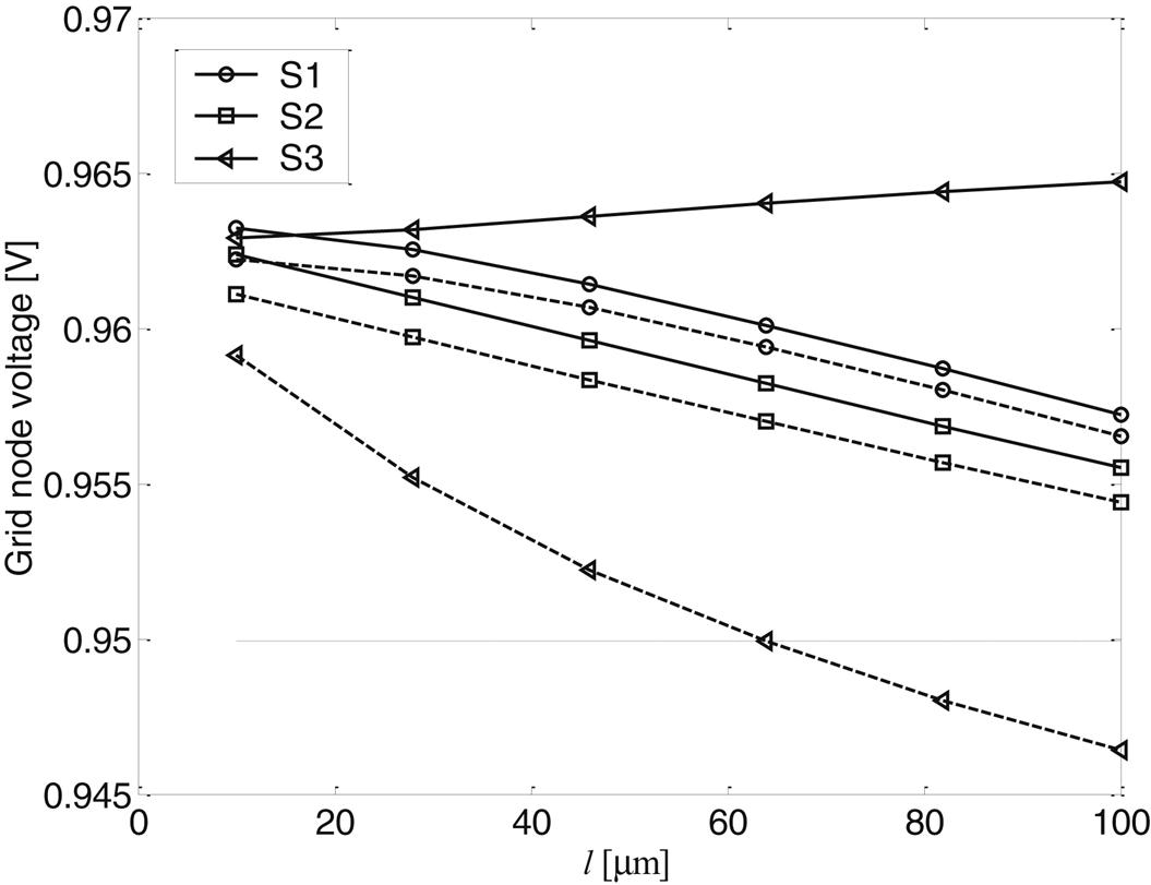
A negligible increase (~5 mV) of the voltage at the TSV location is noted, as shown by the solid curve with increasing l. This counterintuitive behavior can be explained by considering the current that flows through the TSV path and the neighboring paths through the stacked vias. As l increases, the impedance of each M1 segment becomes comparable to the impedance of a stack of vias. Consequently, the current that flows through the TSV and M1 decreases. Alternatively, the current that flows through M6 to the TSV stacked vias increases. This change in the flow of current causes the voltage to increase at the TSV node with increasing l.
The decrease in the voltage drop due to the TSV path can be used to improve routability within a tier. This improvement is important since TSVs greatly increase routing congestion. To demonstrate that a smaller number of stacked vias within the power grid is required when the TSV path is considered, the stacked vias are removed within increasing radius from the TSV notated as d. The resulting voltage drop is depicted in Fig. 18.26 where l=30 μm. Note that fewer paths provide current to the transistors. Since the stacked vias are removed from the grid, the TSV path supports greater current. The voltage drop specification is therefore maintained up to d=3 or, equivalently, with 22% fewer intratier vias (see the dashed curves in Fig. 18.26).

The stacked vias are also removed from the grid when the TSV path is not present. The voltage drop on this grid is also shown in Fig. 18.26 by the solid curves. In this grid, the TSV is not connected to M1 and, consequently, the voltage drop rapidly increases as the stacked vias are removed to decrease routing congestion.
In the second scenario, only three sources switch. These three sources are located at the upper left corner of the grid (S1) and at the adjacent nodes (in the east and west direction) of the node where the TSV is connected (S2). The peak current of these sources is IL=8 mA, while the rise and fall times are the same as in the previous scenario. The voltage drop at these current sources (i.e., S1, S2) and the center of the M1 grid (S3) is depicted in Fig. 18.27. The voltage drop within the two grids with (solid curves) and without (dashed curves) the TSV path is illustrated. The simulation results indicate that the additional path again decreases the voltage drop for this current source configuration. The locality of the TSV path is also demonstrated, since the voltage drop at the remote current source (S1) does not significantly change when the length of the grid segment is varied. Note the solid and dashed curves for S1 denoted by the circles in Fig. 18.27, which are practically indistinguishable.

These local power distribution paths can also decrease the extrinsic or intentional decoupling capacitance used to compensate for the voltage drop on the power grid. For the first scenario, the peak current of the sources is increased to IL=1 mA, while the decoupling capacitors satisfy the voltage drop constraint. The decoupling capacitance is listed in Table 18.3 where the TSV path is both present and not present. The grid including the TSV path requires 25% less capacitance to satisfy the voltage drop constraint, an important savings in the area of a tier within a 3-D system.

18.3.2 Effect of Through Silicon Via Tapering on Power Distribution Networks
In all of the power delivery schemes presented in Section 18.1 and the models of 3-D power distribution networks discussed in Section 18.2, the TSVs contribute to the power supply noise along the vertical flow of current within a 3-D circuit. To lower the parasitic impedance of the TSV, one approach is to increase the number and/or diameter of the TSVs, which increases the area occupied by these interconnects. These approaches assume that the same number and size of TSVs are employed within each tier. This constraint is however a strict and inappropriate constraint as the overall current carried by the TSVs within each tier is not the same.
Those TSVs within the tiers closer to the package typically carry current drawn from all of the other tiers. The TSVs in the upper tiers closer to the heat sink carry an increasingly lower current (assuming all of the tiers are active). This behavior supports the use of a nonuniform radius for the TSVs across the 3-D stack. For those tiers closer to the package, the TSVs exhibit a greater diameter [673], as illustrated in Fig. 18.28A. Although uniform sizing can be applied to all of the TSVs, uniform sizing wastes silicon area in those tiers where the TSVs carry less current.

The TSVs, however, constitute primary paths for the flow of heat within 3-D circuits, as discussed in Chapter 12, Thermal Modeling and Analysis. By following this same approach, to resize the TSVs to ensure the efficient flow of heat throughout a 3-D stack, increasing TSV sizing occurs in the opposite direction as compared to sizing TSVs for controlling power supply noise [673]. The electrical and thermal networks are separately evaluated to determine the optimum TSV size to satisfy each of these objectives. From this evaluation, those sizes that satisfy both objectives (without being optima for each individual objective) are selected, as illustrated in Fig. 18.28B.
A Thevenin network is utilized to determine the TSV size, where the same current through each tier is assumed. The maximum TSV resistance for the minimum TSV radius allowed by the target fabrication process is also known. By sweeping the TSV radius (or by applying an optimization method), the optimal TSV size to satisfy voltage constraints and minimize the area of the TSVs is determined. In a similar manner, the size of the TSVs to satisfy the temperature constraints is determined where the thermal resistance is utilized in this case.
To demonstrate the effects of nonuniform sizes of the TSVs, an exemplary 3-D circuit with ten tiers is considered [673]. Two different sizing ratios are considered. In the first case, the tapering step is 2 μm (Case 1), while in the second case, the tapering step is 0.2 μm (Case 2). In both cases, a minimum radius of a TSV of 1 μm is assumed. To satisfy both the thermal and power supply noise objectives, the resulting radii of the TSVs for the two cases are: (1) R9–10=9 μm, R8–9=7 μm, R7–8=5 μm, R6–7=3 μm, R5–6=1 μm, R4–5=3 μm, R3–4=5 μm, R2–3=7 μm, and R1–2=9 μm for the tapering step of 2 μm; (2) R9–10=1.8 μm, R8–9=1.6 μm, R7–8=1.4 μm, R6–7=1.2 μm, R5–6=1 μm, R4–5=1.2 μm, R3–4=1.4 μm, R2–3=1.6 μm, and R1–2=1.8 μm for the tapering step of 0.2 μm.
Comparing these two cases with the case of uniform sizing across all of the tiers within this stack, the uniform TSVs yield a voltage drop of 90 mV for the TSV farthest from the package tier. For Case 1, the noise in the same tier is only 65 mV [673]. Furthermore, the noise in Case 1 is lower than in Case 2, demonstrating that a relatively small difference in TSV radius produces limited gains. The temperature also drops when a nonuniform radius is applied to the TSVs. Similarly, the temperature decreases from 43°C to 30°C for the tier located farthest from the heat sink if tapering is applied. The drop in temperature due to the use of nonuniform TSVs is considerable. In addition, a greater tapering step will further lower the temperature.
Another well known method to limit power supply noise is the use of decoupling capacitance. Techniques for allocating decoupling capacitance within 3-D circuits are discussed in the following section, where the contribution of a decoupling capacitance from neighboring tiers to decrease power supply noise in some other tier is described.
18.4 Decoupling Capacitance for Three-Dimensional Power Distribution Networks
Decoupling capacitors are an indispensable component at every level of the power distribution system. In on-chip power distribution networks, this capacitance is achieved by either a MOS capacitance or a MIM capacitance [325]. The typical difference between the two types of on-chip decoupling capacitances is a MOS capacitor provides a higher density capacitance at the expense of higher leakage current as compared to a MIM capacitor [687]. Trench decoupling capacitors can also be used as an alternative to reduce the leakage current of a MOS capacitance although this technology is fairly expensive [688]. Typical decoupling capacitors are efficient for a small distance from the switching load. This effective distance has been analyzed for 2-D systems [686]. For 3-D circuits, however, the decoupling capacitance of an adjacent tier can be located within a distance of tens of micrometers from the switching load due to the short and low resistive path of the TSVs. Allocation of the decoupling capacitance within a 3-D system should therefore consider the overall 3-D stack rather than individual tiers.
To explore the effects of the decoupling capacitance among the tiers, some simple cases are discussed based on the analytic model of power supply noise presented in Section 18.2. These systems consist of a varying number of tiers, where each tier is an Intel microprocessor manufactured in a 65 nm CMOS technology node [678]. Each tier comprises five circuit blocks with the same footprint and the same current density of 100 A/cm2 [674]. All of the blocks switch simultaneously to produce the worst case power supply noise. The current waveform is a ramp function with a rise time of 0.7 ns.
The power network contains 43 power (ground) tracks between each pair of power (ground) pads. The resistance of a wire segment Rw in (18.8) is 0.22 Ω. The inductance of the package pins is 0.5 nH. The TSVs are 200 μm in height with a diameter of 50 μm. The effective inductance (one half of the loop inductance) for one TSV is determined from an EM solver as 0.06 nH. Finally, 20% of each tier is assumed to be available for the MOS decoupling capacitors.
Several scenarios illustrated in Fig. 18.29 are evaluated in terms of the worst case power supply noise. The 2-D system (single tier) exhibits the lowest noise, Vdrop=182 mV, as shown in Fig. 18.29A. Stacking these tiers increases the noise in the topmost tier (farthest from the package pins) to 400 mV, as depicted in Fig. 18.29B. Adding a fifth tier as a decoupling capacitance tier adjacent to the package, as illustrated in Fig. 18.29C, decreases this noise by 22% to 312 mV. The rationale for placing this tier close to the package is to offer a low recharge time for the decoupling capacitance. The efficiency of the decoupling capacitance tier however is highest if this tier is placed on the top of the 3-D stack, as shown in Fig. 18.29D. In this case, the noise is 256 mV.

Although the noise decreases, this noise is considerably higher than in the single tier case. The use of a second tier as a decoupling capacitance is depicted in Fig. 18.30 to further lower the noise. As shown in Figs. 18.30B and C, interleaving the decoupling capacitance tiers with the processor tiers does not yield the lowest noise. Rather, placing both of these tiers on top of the stack, as illustrated in Fig. 18.30D, produces the lowest noise Vdrop-3D=199 mV, which is much closer to the noise produced by a 2-D system.

In each of these scenarios, the decoupling capacitance is the same across each tier which may not be possible for several reasons. These reasons include, for example, the limited whitespace for the decoupling capacitance in each tier, the different technology nodes among the tiers, and the operating conditions of the circuits. A particular situation arises when the circuits in the adjacent tiers are power gated to save power. In these cases, the decoupling capacitance (intentional or intrinsic) from these tiers is no longer available since those transistors act as power switches that isolate this capacitance from the power distribution network of the overall system. This situation enhances the beneficial effects of the capacitance from the neighboring tiers. Specific topologies that overcome this variation in decoupling capacitance are discussed in the following subsection.
18.4.1 Decoupling Capacitance Topologies for Power Gated Three-Dimensional ICs
Power gating is a broadly used technique to greatly reduce the power of an integrated system. Those circuits that do not perform a task during a certain time are temporarily disconnected from the power supply to eliminate leakage and dynamic current. Large transistors, usually called “sleep transistors,” disconnect the power supply rails from the “virtual” power supply which is connected to the circuits [689]. A side effect of power gating is the decrease in the overall capacitance of the system. Consequently, the capacitance in these circuits cannot behave as decoupling capacitors and help alleviate abrupt current surges in adjacent circuits. This situation is more subtle in 3-D circuits for two reasons. First, due to the potentially greater power densities as compared to 2-D circuits, low power methods, such as power gating, may be applied more aggressively. Second, the short and low impedance vertical paths provided by the TSVs enable the capacitance of adjacent tiers to more effectively satisfy abrupt current demands within a tier.
Another aspect of power gating is the process of transitioning the power gated circuit to an operating state. If several circuits simultaneously transition to an active state, the sudden current demand can cause a significant dip in the power supply voltage. This voltage drop appears as power supply noise on nearby active circuits [690]. Considering these two issues, methodologies to effectively utilize decoupling capacitance in 3-D circuits are discussed in this subsection.
A topology that allows the decoupling capacitance to be utilized despite the circuit block being power gated is illustrated in Fig. 18.31 [691]. The primary difference from a standard power gated circuit is that the decoupling capacitor is connected both to the global voltage supply and to the virtual power rail through two switch transistors, which select one of the two power lines.

If transistor switch 2 is on and switch 1 is off, the decoupling capacitor is connected to the virtual Vdd. If the circuit is active, the sleep transistors are on, and the decoupling capacitor provides charge to the local circuit blocks, shown in Fig. 18.31, rather than to more distant circuits as the path to the Vdd rail is more resistive. Alternatively, if the circuit is power gated, switch 2 is off and switch 1 is on, the decoupling capacitor supplies charge to the other circuits, disconnecting the Vdd rail from the virtual power supply.
A tradeoff between the switch transistor and decoupling capacitor exists for this topology as the overall area overhead from these components should be as small as possible while satisfying any voltage constraints. Further increasing the decoupling capacitance is not useful as the area and, consequently, the on-resistance of the switch transistors is high, limiting the efficiency of the capacitor. Alternatively, if the switch transistor is large, lowering the impedance of the discharge path of the capacitor, the leakage current is greater. Therefore, choosing an appropriate size for these two components is required to achieve a decoupling capacitor system with the highest efficiency.
Another topology for connecting the decoupling capacitance is illustrated in Fig. 18.32, where the decoupling capacitor is directly connected to the Vdd rail. The capacitor provides sufficient charge to the adjacent circuits irrespective of whether the local circuit blocks are power gated. The discharge path for the local circuit blocks, however, includes the sleep transistor. Consequently, this topology can exhibit greater power supply noise as compared to the reconfigurable topology shown in Fig. 18.31. As the sleep transistors, however, are typically large (the equivalent transistor width is on the order of millimeters), the voltage drop across these devices is extremely small.

To evaluate the efficiency and explore tradeoffs between these two topologies, a power grid for a 3-D circuit with three tiers is considered. The topmost tier is connected to a package with C4 connections. Ten metal layers are used in this topology [693]. The top two layers are the global power grid, and layers 7 and 8 are the virtual grid. In addition, a via-last manufacturing process for the TSVs is assumed. The grid is 1 mm×1 mm. The segments of the power grid and the TSVs are modeled with multiple RLC π segments. The C4 connections are modeled as RL sections. Furthermore, the load consists of an inverter pair of different size distributed across the circuit. Finally, the voltage drop constraint is set to 5% of Vdd, 50 mV.
As the 3-D circuit includes three tiers, several scenarios with one or more active tiers are evaluated. These scenarios are listed in columns 1 to 3 of Table 18.4 where the maximum power supply noise for all of these scenarios is also listed. The decoupling capacitance ensures that the voltage constraint is satisfied for the standard topology with all tiers active (and, consequently, connected to global Vdd). As reported in Table 18.4, for the other scenarios where some tiers are power gated, the traditional topology violates the voltage constraint. This behavior is due to the lower decoupling capacitance available across the entire 3-D stack. Alternatively, both of the other topologies exhibit a considerably smaller power supply noise.
Table 18.4
Peak Voltage Noise for Different Scenarios of Activity Among the Three Tiers of a 3-D Circuit for the Standard, Reconfigurable, and Always On Topologies of Decoupling Capacitance [692]
| Operating State of Tiers | Power Supply Noise of Decoupling Capacitance Topologies (mV) | ||||||
| Top Tier | Middle Tier | Bottom Tier | Standard | Reconfigurable | Always On | ||
| Decrease | Decrease | ||||||
| On | On | On | 50 | 50 | – | 50 | – |
| On | Off | On | 48.16 | 43.48 | 9.7% | 43.40 | 9.9% |
| Off | Off | On | 52.22 | 39.64 | 24.1% | 38.07 | 27.1% |
| Off | On | On | 48.55 | 44.50 | 8.3% | 42.89 | 11.7% |
| Off | On | Off | 52.51 | 38.78 | 26.1% | 37.55 | 28.5% |

Another important parameter that affects power noise in power gated circuits is the wake-up time of the inactive circuits, which affects the operation of the active systems. This behavior is common to both 2-D and 3-D circuits. A straightforward method to decrease the current demand during the wake-up process (the transition from the power gated to the operating state) is to slightly delay the turn-on time of the sleep transistors to ensure that the drawn current increases at a slower rate. A daisy chain of buffers is utilized for this approach, as illustrated in Fig. 18.33. The drawback of this approach, however, is the prolonged wake-up time of the circuit. To avoid this situation, a wake-up controller initiates the wake-up process in two steps, where a small number of sleep transistors is switched on, followed by the remaining transistors switching on [694]. The duration of each step is constant and is typically several clock cycles.

This two step method is also applicable to 3-D circuits; however, the situation is more complicated since the power supply noise exhibited on each tier strongly depends upon the location of the tier within the stack [695]. For 3-D stacks assuming that each tier is either active, inactive, or transitions to the active state, several cases exist where the power supply noise varies across all of the possible operating scenarios. Different wake-up times are therefore used between the two steps depending upon the tier that transitions to the active state and the tiers that are already active. This information is utilized to guide an adaptive wake-up controller, where the time duration of each step is carefully controlled [695]. The objective of this adaptive controller is to reduce the total wake-up time, while satisfying any power supply noise constraints.
This adaptive two step wake-up controller has been evaluated for a 3-D circuit with five tiers, where a 22 nm technology node is assumed. In the first step, 5% of the sleep transistors are switched on, whereas the remaining transistors are switched on during the second step. The duration of each step, however, is adjusted according to the operating conditions of the overall 3-D stack. A comparison of the efficiency of the wake-up controller is performed with both constant and adaptive steps. The adaptive controller exhibits an average decrease of 28% in the wake-up time of the 3-D stack, without violating the power supply noise constraint. Although not discussed here, the number of sleep transistors switched on between the two steps is another variable to control the wake-up time at the expense of a more highly complex controller.
18.5 Wire Sizing Methods in Three-Dimensional Power Distribution Networks
A straightforward approach to design a 3-D power distribution network is to independently generate a power network for each tier of the stack and connect these networks with TSVs. Unfortunately, this approach does not consider several traits of 3-D power distribution networks, leading to suboptimal networks that either do not satisfy the power supply noise constraints throughout the stack or results in overdesign, wasting vital interconnect and power resources.
As described in the previous sections of this chapter, the behavior of 3-D power distribution networks depends on the number and size of the TSVs, the TSV technology, and the decoupling capacitance of the adjacent tiers. These features are relevant only to 3-D circuits. Moreover, most case studies are based on simple assumptions. Although these assumptions are useful to understand the behavior of 3-D power distribution networks, more formal techniques are required.
Optimizing power distribution networks for 3-D systems requires consideration of several parameters in addition to the parameters of 2-D circuits, such as the size of the horizontal wires. Moreover, specific assumptions, such as uniform power dissipation for each tier should be relaxed to consider more practical cases. An algorithm which optimizes the area of the power network within each tier while simultaneously satisfying global power noise and thermal objectives throughout a 3-D system is presented in this section. Several other constraints are also added to the optimization process.
The power supply noise objective of the algorithm is
(18.44)
where Vdropmax for all tiers is the overall noise allowed across the system. The term ![]() is the total conductance of all of the TSVs connecting tier i−1 to tier i (for i>1). The current flowing through each of these TSVs is denoted by Ij. Furthermore, the bonding style is face-to-back, which implies that the topmost global layer of a tier connects by TSVs to the bottommost local layer in the next tier. For this bonding approach,
is the total conductance of all of the TSVs connecting tier i−1 to tier i (for i>1). The current flowing through each of these TSVs is denoted by Ij. Furthermore, the bonding style is face-to-back, which implies that the topmost global layer of a tier connects by TSVs to the bottommost local layer in the next tier. For this bonding approach, ![]() notates the total impedance from all of the metal layers of the power network within each tier.
notates the total impedance from all of the metal layers of the power network within each tier.
For the three tier circuit shown in Fig. 18.34, the corresponding constraints for the power supply noise based on (18.44) are [472]
(18.45)
(18.46)

and
(18.47)
where the term relating to the resistive voltage drop of the TSVs is not included in (18.45) since this tier is the bottommost tier connected to the package.
An expression for the temperature constraint is similar to (18.44) based on the electro-thermal duality, and is [472]
(18.48)
where max_ΔTbetween tiers is the maximum allowed temperature difference between the uppermost and bottom tiers. The term ![]() denotes the total thermal resistance of all of the TSVs connecting two adjacent tiers. The heat produced within a tier i is notated as Qi. These constraints for the power supply noise and temperature, respectively, facilitate the analysis of the optimization problem as the size of the power grid and TSVs of each tier are treated separately. Satisfaction of these constraints (see, for example (18.44)) ensures that the noise and temperature limits are maintained across the entire 3-D stack.
denotes the total thermal resistance of all of the TSVs connecting two adjacent tiers. The heat produced within a tier i is notated as Qi. These constraints for the power supply noise and temperature, respectively, facilitate the analysis of the optimization problem as the size of the power grid and TSVs of each tier are treated separately. Satisfaction of these constraints (see, for example (18.44)) ensures that the noise and temperature limits are maintained across the entire 3-D stack.
With these constraints and utilizing the electro-thermal model presented in Section 18.2.1 to determine the temperature and voltage at any node within the power distribution network of a 3-D circuit, the problem of optimizing resources in these networks is stated as follows. Minimize the cost function,
(18.49)
to ensure that the following constraints are satisfied [472]:
(C1) for the voltage of the node q in tier i (see (18.34) and (18.44)),
(18.50)
(C2) for the voltage of the node q in tier i (see (18.41) and (18.48)),
(18.51)
(C3) for the width of the power and ground lines,
(18.52)
(C4) for the diameter of the TSVs,
(18.53)
(C5) for ensuring reliability, an electromigration constraint can be added (see (18.36)) where
(18.54)
and (C6) is a constraint that emphasizes either the voltage drop or the temperature objective. The weighted function is
(18.55)
In the cost function (18.49), wtrack is the width of the horizontal wire tracks within the power distribution network within each tier, and DTSV is the diameter of the TSVs within each tier. Note that the TSVs at different tiers can have different diameters but the TSVs within a tier are all uniformly sized. The coefficient β is a weighting factor to determine the significance of each term in (18.49). The overall optimization process is illustrated in Fig. 18.35. Since the tiers towards the middle of the stack are more sensitive to power supply noise and thermal issues, the TSV sizing process is initially applied only to these tiers, as shown in Fig. 18.35A [472]. The resulting TSV diameter for these tiers is a lower bound for the other tiers, denoted as D*min (see C4). Note also that in step 4 of the algorithm depicted in Fig. 18.35C, the objectives OVqdrop and OTq are dimensionless. If any of these objectives is equal to unity, the maximum allowed voltage drop or temperature has been achieved.


Per the cost function given by (18.49), the algorithm minimizes the area of the horizontal and vertical wires while simultaneously satisfying the objectives, OVqdrop and OTq. The diameter of the TSVs has a lower bound that is not set by the specifications of the technology but rather from the TSV diameter in the middle tiers D*min. In the flowchart depicted in Fig. 18.35B, the width of each horizontal wire within the power network of a tier is successively reduced, ensuring constraints C1 to C6 are not violated. This procedure is also applied to the TSVs and is iterated across all of the tiers. The algorithm terminates when any horizontal wire or TSVs within a tier can no longer be decreased without violating constraints C1 to C6.
This optimization algorithm is applied to a 3-D circuit with three tiers where the allowed voltage drop is 100 mV (10% of Vdd) and the allowed temperature difference between the two extreme tiers is 10°C. The ambient temperature is assumed to be 27°C. To demonstrate the effects of parameter a, the power density is set the same for all tiers. The applied power density in this case is 0.6 μW/μm2. If temperature is emphasized (a=0), the savings in area reaches 43%. If supply noise is the primary focus (a=1), the savings in area reaches 55%. For equally important voltage drop and temperature constraints (a=0.5), the savings in area is 53%. The greatest savings in area is produced for a=0.9.
The algorithm is also evaluated for several power densities to reflect different levels of power dissipation among tiers. The following power densities are considered: (1) 1.5 μW/μm2 as the high power density, (2) 1 μW/μm2 as the medium power density, and (3) 0.8 μW/μm2 as the low power density. For β=1 and a=0.5, the area savings for the different cases of power densities are reported in Table 18.5. In columns 3 and 5, the listed objectives correspond to the use of wmax for all metal layers within the power distribution network. In columns 4 and 6, the same objectives are reported where the optimization algorithm is applied.
Table 18.5
Savings in Area for Several Cases of Nonuniform Power Density Among the Three Tiers [472]
| OVdrop | OT | ||||||
| Case # | Tier 3–Tier 2–Tier 1 | Before | After | Before | After | Area Savings | Run Time (s) |
| 1 | High–medium–low | 0.87 | 1 | 0.46 | 0.56 | 25.0% | 1440 |
| 2 | High–low–medium | 0.91 | 1 | 0.50 | 0.56 | 20.0% | 2160 |
| 3 | Medium–high–low | 0.91 | 1 | 0.56 | 0.61 | 18.3% | 1550 |
| 4 | Medium–low–high | 0.84 | 1 | 0.60 | 0.72 | 26.7% | 1550 |
| 5 | Low–medium–high | 0.79 | 1 | 0.63 | 0.82 | 33.3% | 1780 |
| 6 | Low–high–medium | 0.87 | 1 | 0.58 | 0.70 | 26.7% | 1200 |
| 7 | High–high–high | 0.98 | 1 | 0.66 | 0.70 | 8.0% | 900 |
| 8 | Medium–medium–medium | 0.88 | 1 | 0.45 | 0.90 | 36.0% | 780 |
| 9 | Low–low–low | 0.86 | 1 | 0.34 | 0.82 | 41.0% | 1140 |

In all of the reported cases, the algorithm produces a wire size that satisfies the voltage drop target, while the temperature is considerably less than originally specified. This situation indicates that the wires can be further decreased in size without violating the maximum temperature constraint. Any further decrease in size will however violate the voltage drop constraint. The resulting gains in area, however, are considerable, reaching 41%.
18.6 Summary
The behavior and related models and design issues for 3-D power distribution systems are discussed in this chapter. The primary concepts are summarized below:
• Vertical integration of the tiers affects power distribution networks in two ways. First, the horizontal dimensions of the power distribution network and the number of P/G package pins are significantly reduced as compared to the footprint of a 2-D circuit. Second, the power distribution networks within the different tiers are connected with TSVs with different electrical characteristics as compared to the horizontal wires.
• Integrating DC–DC converters into a 3-D stack greatly decreases the interconnect parasitic impedance of the power supply and logic tiers, improving the overall efficiency of the power delivery system.
• For a large number of tiers, integrating converters within the tiers at the ends of the stack lowers the voltage drop by more than 75% as compared to using converters in only one tier.
• An alternative power delivery method called “multi-level” utilizes differential rails of supply voltages between adjacent tiers. The primary advantage of the multilevel approach is that charge is recycled among differential pairs of power supply rails, greatly reducing the power supply noise.
• Several challenges relating to multi-level power delivery exist. The primary challenge is to maintain balanced currents among the tiers.
• Several models for 3-D power distribution networks have been developed to support design space exploration. These models range from closed-form analytic models based on the continuous plane approximation for the power and ground grids to compact models that replace segments of the power grids and TSVs with passive impedance sections.
• Models of the power distribution network within the memory tiers are more sensitive to substrate losses as the metal layers in these circuits are close to the substrate. These losses should therefore be included within the models.
• Electro-thermal models are based on the duality of voltage to temperature and current to heat flux to efficiently analyze power distribution networks.
• TSVs efficiently distribute power and ground in 3-D systems. Coaxial TSVs can half the number of TSVs used for P/G distribution in addition to reducing the required decoupling capacitance.
• Via-first and via-middle TSV technologies support ancillary paths that can improve local power integrity. These paths decrease routing congestion, save area, or lower the added decoupling capacitance.
• Nonuniform TSV diameters among tiers facilitates both power and thermal integrity.
• The low impedance of the TSV paths allows the decoupling capacitance of a tier to provide charge to the switching circuits in other tiers. The tiers contain decoupling capacitance for the neighboring circuits, where this capacitance is more efficient if placed farthest from the package.
• Power gating disconnects the neighboring decoupling capacitance, degrading power integrity. Specific circuits with low overhead can avoid this situation.
• A controller adapts the switching pattern and wake-up time of the sleep transistors. This technique avoids high current demands when the circuits transition from a power gated state to an operating state.
• Power and thermal integrity in 3-D systems is achieved by iteratively optimizing the power network of each tier to satisfy global constraints across the 3-D stack.
• An iterative algorithm, where the width of the horizontal P/G wires and the diameter of the TSVs are reduced, provides a means to satisfy noise and temperature constraints while reducing wire area.