
Chapter 27
Programmable Logic to ASICs
Programmable devices have progressed through a long evolution to reach the complexity today to support an entire system on a chip (SOC). This chapter gives an approximately chronological discussion of these devices from least complex to most complex. I say “approximately” because there is definitely overlap between the various devices, which are still in use today. The chapter includes a discussion on application-specific integrated circuits (ASICs) and how CPLDs and FPGAs fit within the spectrum of programmable logic and ASICs.
The objectives of this chapter are to become aware of the different programmable devices available and how they led to the current state-of-the-art device. These objectives are summarized here:
• Learn the history of programmable devices.
• Obtain a basic knowledge of the technologies of programmable devices.
• Understand the architectures of earlier programmable devices.
• Discover the speed, power, and density limitations of earlier programmable devices.
• Appreciate the needs that arose and that were not addressed by existing devices, and that created a market for CPLDs and FPGAs.
NOTE: The ROM cell
The basic diagram for a ROM cell containing a single bit of data is shown in Figure 27.1. The word line is turned on if the address into the chip includes this particular bit cell. The metal layer is used to program the data into the ROM during fabrication. In other words, if the metal layer mask has a connection between the transistor output and the data line, the bit is programmed as a zero. When the bit is addressed, the output will be pulled to a low voltage, a logical zero. If there is no connection, the data line will be pulled up by the resistor to a high voltage, a logical one.
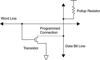
Figure 27.1 The ROM cell
27.1 Programmable Read-Only Memory (PROM)
The first field-programmable devices were created as alternatives to expensive mask-programmed ROM. Storing code in a ROM was an expensive process that required the ROM vendor to create a unique semiconductor mask set for each customer. Changes to the code were impossible without creating a new mask set and fabricating a new chip. The lead time for making changes to the code and getting back a chip to test was far too long.
PROMs solved this problem by allowing the user, rather than the chip vendor, to store code in the device using a simple and relatively inexpensive desktop programmer. This new device was called a programmable read-only memory (PROM). The process for storing the code in the PROM is called programming, or burning the PROM. PROMs, like ROMs, retain their contents even after power has been turned off.
Note: One-time programmable PROM cells
One-time programmable PROMs rely on an array of fuses and either diodes or transistors, as shown in Figure 27.2 and Figure 27.3. These fuses, like household fuses, consist of a wire that breaks connection when a large amount of current goes through it. To program a one-bit cell as a logic one or zero, the fuse for that cell is selectively burned out or left connected.

Figure 27.2 One-time programmable, diode-based PROM cell
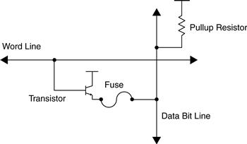
Figure 27.3 One-time programmable, transistor-based PROM cell
Although the PROMs were initially intended for storing code and constant data, design engineers also found them useful for implementing logic. The engineers could program state machine logic into a PROM, creating what is called microcoded state machines. They could easily change these state machines in order to fix bugs, test new functions, optimize existing designs, or make changes to systems that were already shipped and in the field.
Eventually, erasable PROMs were developed which allowed users to program, erase, and reprogram the devices using an inexpensive, desktop programmer. Typically, PROMs now refer to devices that cannot be erased after being programmed. Erasable PROMS include erasable programmable read only memories (EPROMs) that are programmed by applying high-voltage electrical signals and erased by flooding the devices with UV light. Electrically erasable programmable read only memories (EEPROMs) are programmed and erased by applying high voltages to the device. Flash EPROMs are programmed and erased electrically and have sections that can be erased electrically in a short time and independently of other sections within the device. For the rest of this chapter, I use the term PROM generically to refer to all of these devices unless I specifically state otherwise.
NOTE: Reprogrammable PROM cells
Reprogrammable PROMs essentially trap electric charge on the input of a transistor that is not connected to anything. The input acts like a capacitor. The transistor amplifies the charge. During programming, the charge is injected onto the transistor by one of several methods, including tunneling and avalanche injection. This charge will eventually leak off. In other words, some electrons will gradually escape, but the leakage will not be noticeable for a long time, on the order of ten years, so that they remain programmed even after power has been turned off to the device. Programming one of these devices causes wear and tear on the chip while the electrons are being injected. Most devices can be programmed about 100,000 times before they begin to lose their capability to be programmed.
PROMs are excellent for implementing any kind of combinatorial logic with a limited number of inputs and outputs. Each output can be any combinatorial function of the inputs, no matter how complex. As I said, this isn’t usually how engineers use PROMs in today’s designs; they’re used to hold bytes of data. However, if you look at Figure 27.4, you can see how each address bit for the PROM can be considered a logic input. Then, simply program each data output bit to have the value of the combinatorial function you are creating. Some early devices used PROMs in this way to create combinatorial logic.

Figure 27.4 A) combinatorial logic, B) equivalent PROM, C) logic values
For sequential logic, one must add external clocked devices such as flip-flops or microprocessors. A simplified example of a state machine built using a PROM is shown in Figure 27.5. The PROM is used to combine inputs with bits representing the current state of the machine, to produce outputs and the next state of the machine. This allows the creation of very complex state machines. Microcode is often decoded within a microprocessor using this method, where the microcode for controlling the various stages of the microprocessor is stored in ROM.
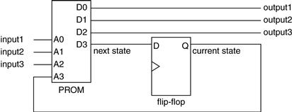
Figure 27.5 PROM-based state machine
The problem with PROMs is that they tend to be extremely slow—even today, access times are on the order of 40 nanoseconds or more—so they are not useful for applications where speed is an issue. These days, speed is always an issue. Also, PROMs are not easily integrated into logic circuits on a chip because they require a different technology and therefore a different set of masks and processes than for logic circuits. Integrating PROMs onto a chip with logic circuitry involves extra masks and extra processing steps, all leading to extra costs.
27.2 Programmable Logic Arrays (PLAs)
Programmable logic arrays (PLAs) were a solution to the speed and input limitations of PROMs. PLAs consist of a large number of inputs connected to an AND plane, where different combinations of signals can be logically ANDed together according to how the part is programmed. The outputs of the AND plane go into an OR plane, where the terms are ORed together in different combinations and finally outputs are produced, as shown in Figure 27.6. At the inputs and outputs there are inverters (not shown in the figure) so that logical NOTs can be obtained. These devices can implement a large number of combinatorial functions, but, unlike a PROM, they can’t implement every possible mapping of their input set to their output set. However, they generally have many more inputs and are much faster.

Figure 27.6 PLA architecture
As with PROMs, PLAs can be connected externally to flip-flops to create state machines, which are the essential building blocks for all control logic.
Each connection in the AND and OR planes of a PLA could be programmed to connect or disconnect. In other words, terms of Boolean equations could be created by selectively connecting wires within the AND and OR planes. Simple high level languages — ABEL, PALASM, and CUPL — were developed to convert Boolean equations into files that would program these connections within the PLA. These equations looked like this:
to represent the logic for:
This added a new dimension to programmable devices in that logic could now be described in readable programs at a level higher than ones and zeroes.
27.3 Programmable Array Logic (PALs)
The programmable array logic (PAL) is a variation of the PLA. Like the PLA, it has a wide, programmable AND plane for ANDing inputs together. The AND plane is shown by the crossing wires on the left in Figure 27.7. Programming elements at each intersection in the AND plane allow perpendicular traces to be connected or left open, creating “product terms,” which are multiple logical signals ANDed together. The product terms are then ORed together. The Boolean equation in Figure 27.8 has four product terms.

Figure 27.7 PAL architecture

Figure 27.8 Boolean equation with four product terms
In a PAL, unlike a PLA, the OR plane is fixed, limiting the number of terms that can be ORed together. This still allows a large number of Boolean equations to be implemented. The reason for this can be demonstrated by DeMorgan’s Law, which states that a | b = !(!a & !b) or A OR B is equivalent to NOT(NOT A AND NOT B).
That means if you use inverters on the inputs and outputs, you can create all the logic you need with either a wide AND plane or a wide OR plane, but you don’t need both.
Including inverters reduced the need for the large OR plane, which in turn allowed the extra silicon area on the chip to be used for other basic logic devices, such as multiplexers, exclusive ORs, and latches. Most importantly, clocked elements, typically flip-flops, could be included in PALs. These devices were now able to implement a large number of logic functions, including clocked sequential logic needed for state machines. This was an important development that allowed PALs to replace much of the standard logic in many designs. PALs are also extremely fast. With PALs, high-speed controllers could be designed in programmable logic.
Notice the architecture of a PAL, shown in Figure 27.7. The AND plane is shown in the upper-left corner as a switch matrix. The dots show where connections have been programmed. The fixed-size ORs are represented as OR gates. A clock input is used to clock the flip-flops. The outputs of the flip-flops can be driven off the chip, or they can be fed back to the AND plane in order to create a state machine.
The inclusion of extra logic devices, particularly flip-flops, greatly increased the complexity and potential uses of PALs, creating a need for new methods of programming that were flexible and readable. Thus the first hardware description languages (HDLs) were born. These simple HDLs included ABEL, CUPL, and PALASM, the precursors of Verilog and VHDL, much more complex languages that are in use today for CPLD, FPGA, and ASIC design.
A simple ABEL program for a PAL is shown in Listing 27.1. Don’t worry about trying to understand the details—it’s for illustration purposes only. Notice that the programming language allows the use of simulation test vectors in the code. The simulation vectors are at the end of the program. This simulation capability brought better reliability and verification of programmable devices, something that was critical when CPLDs and FPGAs were developed.
Listing 27.1 A simple ABEL program
FLAG ‘-R3’ , ‘-T1’ , ‘-V’ , ‘-F0’ , ‘-G’ , ‘-Q2’;
!req PIN 3; “Instruction/Data Request from processor
!emacc PIN 4; “Emulator access
opt0 PIN 5; “Opt bit from processor
opt1 PIN 6; “Opt bit from processor
opt2 PIN 7; “Opt bit from processor
a19 PIN 8; “Address bit from processor
a20 PIN 9; “Address bit from processor
a21 PIN 10; “Address bit from processor
a22 PIN 11; “Address bit from processor
a23 PIN 14; “Address bit from processor
a31 PIN 23; “Address bit from processor
!parallel PIN 17; “Parallel port select
!switch PIN 19; “Switches select
!serial PIN 20; “Serial port select
!config PIN 21; “Configuration register select
addr = [a31, a23, a22, a21, a20, a19];
PARALLEL = [0, 1, 0, 1, 0, 0];
SWITCHES = [0, 1, 0, 1, 1, 0];
eprom = req & !emacc & !opt2 & !res & (addr == EPROM);
sram = req & !emacc & !opt2 & !res & (addr == SRAM);
dram:= req & !emacc & !opt2 & !res & (addr >=
parallel := req & !emacc & !opt2 & !res & (addr == PARALLEL);
serial := req & !emacc & !opt2 & !res & (addr == SERIAL);
switch := req & !emacc & !opt2 & !res & !switch & (addr == SWITCHES);
leds := req & !emacc & !opt2 & !res & !leds & (addr == LEDS);
config := req & !emacc & !opt2 & !res & !config & (addr == CONFIG);
[ clk, !res, !oe, !req, !emacc, opt2, opt1, opt0]
-> [eprom,!sram,!dram,!parallel,!serial,!switch,!leds,!config]);
[ c, 0, 0, x, x, x, x, x] -> [ 1, 1, 1, 1, 1, 1, 1, 1];
[ c, 1, 0, 1, x, x, x, x] -> [ 1, 1, 1, 1, 1, 1, 1, 1];
[ c, 1, 0, x, 0, x, x, x] -> [ 1, 1, 1, 1, 1, 1, 1, 1];
[ c, 1, 0, x, x, 1, x, x] -> [ 1, 1, 1, 1, 1, 1, 1, 1];
[!res, !oe, !req, !emacc, opt2, opt1, opt0, a31, a23, a22, a21, a20, a19]
“5” [ 0, 0, x, x, x, x, x, x, x, x, x, x, x] -> [ 1, 1];
[ 1, 0, 1, x, x, x, x, x, x, x, x, x, x] -> [ 1, 1];
[ 1, 0, 0, 1, 0, x, x, 0, 0, 0, 0, 0, 0] -> [ 0, 1];
[ 1, 0, 0, 1, 0, x, x, 0, 0, 0, 0, 0, 1] -> [ 0, 1];
[ 1, 0, 0, 1, 0, x, x, 0, 0, 0, 0, 1, 0] -> [ 1, 0];
Listing 27.2 shows the compiled output from this code, consisting of a map of connections within the device to program in order to obtain the correct functionality.
Listing 27.2 The compiled output
ABEL(tm) 3.00a FutureNet Div, Data I/O Corp. JEDEC file for: P20R6
Created on: 29-Nov-:1 06:52 PM
1111111111111111111111111111111111111111
0110101101111111111110111111101110111010
0000000000000000000000000000000000000000
0000000000000000000000000000000000000000
0000000000000000000000000000000000000000
0000000000000000000000000000000000000000
0000000000000000000000000000000000000000
0000000000000000000000000000000000000000
0110101101011111111110111011101110110101
0000000000000000000000000000000000000000
0000000000000000000000000000000000000000
0000000000000000000000000000000000000000
0000000000000000000000000000000000000000
0000000000000000000000000000000000000000
0000000000000000000000000000000000000000
0000000000000000000000000000000000000000
0110101101111111111110110111101101111001
0000000000000000000000000000000000000000
0000000000000000000000000000000000000000
0000000000000000000000000000000000000000
0000000000000000000000000000000000000000
0000000000000000000000000000000000000000
0000000000000000000000000000000000000000
0000000000000000000000000000000000000000
0110101101111111110110111011011101111001
0000000000000000000000000000000000000000
0000000000000000000000000000000000000000
0000000000000000000000000000000000000000
0000000000000000000000000000000000000000
0000000000000000000000000000000000000000
0000000000000000000000000000000000000000
0000000000000000000000000000000000000000
0110101101111111111110010111011101111001
0000000000000000000000000000000000000000
0000000000000000000000000000000000000000
0000000000000000000000000000000000000000
0000000000000000000000000000000000000000
0000000000000000000000000000000000000000
0000000000000000000000000000000000000000
0000000000000000000000000000000000000000
0110101101111111111110111011101101111001
0000000000000000000000000000000000000000
0000000000000000000000000000000000000000
0000000000000000000000000000000000000000
0000000000000000000000000000000000000000
0000000000000000000000000000000000000000
0000000000000000000000000000000000000000
0000000000000000000000000000000000000000
0110101101111111111110111011111110111001
0110101101111111111110111111101110111001
0110101101111111111110110111011111111110
0110101101111111111110111111111101111110
0110101101111111111110111111111111110110
0000000000000000000000000000000000000000
0000000000000000000000000000000000000000
0000000000000000000000000000000000000000
1111111111111111111111111111111111111111
0110101101111111111110111011011110111010
0000000000000000000000000000000000000000
0000000000000000000000000000000000000000
0000000000000000000000000000000000000000
0000000000000000000000000000000000000000
0000000000000000000000000000000000000000
0000000000000000000000000000000000000000*
V0001 C0XXXXXXXXXN0XHHHHHHHHXN*
V0002 C11XXXXXXXXN0XHHHHHHHHXN*
V0003 C1X0XXXXXXXN0XHHHHHHHHXN*
V0004 C1XXXX1XXXXN0XHHHHHHHHXN*
V0005 X0XXXXXXXXXN0XHNNNNNNHXN*
V0006 X11XXXXXXXXN0XHNNNNNNHXN*
V0007 X101XX00000N00HNNNNNNL0N*
V0008 X101XX01000N00HNNNNNNL0N*
V0009 X101XX00100N00LNNNNNNH0N*
27.4 The Masked Gate Array ASIC
An application-specific integrated circuit, or ASIC, is not a programmable device, but it is important precursor to the developments leading up to CPLDs and FPGAs. An ASIC is a chip that an engineer can design with no particular knowledge of semiconductor physics or semiconductor processes. The ASIC vendor has created a library of cells and functions that the designer can use without needing to know precisely how these functions are implemented in silicon. The ASIC vendor also typically supports software tools that automate such processes as circuit synthesis and circuit layout. The ASIC vendor may even supply application engineers to assist the ASIC design engineer with the task. The vendor then lays out the chip, creates the masks, and manufactures the ASICs.
ASICs can be implemented using one of two internal architectures—gate array or standard cell. The differences between the two architectures are beyond the scope of this book. The standard cell architecture is not as relevant to CPLDs and FPGAs as the gate array architecture, which I describe briefly.
The gate array ASIC consists of rows and columns of regular transistor structures, as shown in Figure 27.9. Around the sides of the chip die are I/O cells containing input and output buffers along with some limited number of transistor. These I/O cells also contain the large bonding pads, shown in the figure, which are simply metal pads that are connected or “bonded” to the external pins of the chip using very small bonding wires.

Figure 27.9 Masked gate array architecture
Within the core array are basic cells, or gates, each consisting of some small number of transistors that are not connected. In fact, none of the transistors on the gate array are initially connected at all. The reason for this is that the connection is determined completely by the design that you implement. Once given a design, the layout software figures out which transistors to connect by placing metal connections on top of the die as shown. First, the low level functions are connected together. For example, six transistors could be connected to create a D flip-flop. These six transistors would be located physically very close to each other. After the low level functions have been routed, they would in turn be connected together. The software would continue this process until the entire design is complete.
The ASIC vendor manufactures many unrouted die that contain the arrays of gates and that it can use for any gate array customer. An integrated circuit consists of many layers of materials, including semiconductor material (e.g., silicon), insulators (e.g., oxides), and conductors (e.g., metal). An unrouted die is processed with all of the layers except for the final metal layers that connect the gates together. Once the design is complete, the vendor simply needs to add the last metal layers to the die to create your chip, using photo masks for each metal layer. For this reason, it is sometimes referred to as a “masked gate array” to differentiate it from a field-programmable gate array.
The advantage of a gate array is that the internal circuitry is very fast; the circuit is dense, allowing lots of functionality on a die; and the cost is low for high volume production. Gate arrays can reach clock frequencies of hundreds of megahertz with densities of millions of gates. The disadvantage is that it takes time for the ASIC vendor to manufacture and test the parts. Also, the customer incurs a large charge up front, called a nonrecurring engineering (NRE) expense, which the ASIC vendor charges to begin the entire ASIC process. And if there’s a mistake, it’s a long, expensive process to fix it and manufacture new ASICs.
27.5 CPLDs and FPGAs
Ideally, hardware designers wanted something that gave them the advantages of an ASIC—circuit density and speed—but with the shorter turnaround time of a programmable device. The solution came in the form of two new devices—the complex programmable logic device (CPLD) and the field-programmable gate array (FPGA). Figure 27.10 shows how CPLDs and FPGAs bridge the gap between PALs and gate arrays. All of the inherent advantages of PALs, shown on the left of the diagram, and all of the inherent advantages of gate array ASICS, shown on the right of the diagram, were combined. CPLDs are as fast as PALs but more complex. FPGAs approach the complexity of gate arrays but are still programmable. CPLD architectures and technologies are the same as those for PALs. FPGA architecture is similar to those of gate array ASICs.
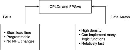
Figure 27.10 The evolution of CPLDs and FPGAs
27.6 Summary
Several programmable and semi-custom technologies preceded the development of CPLDs and FPGAs. This chapter started by reviewing the architecture, properties, uses, and trade-offs of the various programmable devices (PROMS, PLAS, and PALs) that were in use before CPLDs and FPGAs. Later the chapter described ASICs and examined the contribution of a specific type of ASIC architecture called a gate array. The architecture, properties, uses, and trade-offs of the gate array were discussed. Finally, CPLDs and FPGAs were introduced, briefly, as programmable chip solutions that filled the gap between programmable devices and gate array ASICs.
References
1. Logic Design Manual for ASICs. Santa Clara, CA: LSI Logic Corporation; 1989.
2. Davenport Jr Wilbur B. Probability and Random Processes New York, NY: McGraw-Hill Book Company; 1970.
3. Dorf, Richard C, eds. Electrical Engineering Handbook. Boca Raton, FL: CRC Press, Inc., 1993.
4. EDA Industry Working Groups Web site, www.eda.org.
5. Maxfield, Clive. Max. Designus Maximus Unleashed! Woburn, MA: Butter-worth-Heinemann; 1998.
6. Zeidman Bob. Introduction to Verilog Piscataway, NJ: Institute of Electrical and Electronic Engineers; 2000.
7. Zeidman Bob. Verilog Designer’s Library Upper Saddle River, NJ: Prentice-Hall, Inc., 1999.