
Chapter 38
Layout and Grounding for Analog and Digital Circuits
The ratio of digital designers to analog designers is increasing. This is not a news flash. Although the emphasis on digital design is providing significant advances in electronic end products, there is still and will always be a portion of circuit design that interfaces with the analog or real world. Could it be possible that analog layout differs from digital layout techniques? There is some similarity in layout strategies between these two domains. The differences can make an easy circuit layout design less than optimum if you are trying to achieve good results. In this chapter, we will discuss five topics. The first topic covers fundamental similarities and differences between analog and digital layout. Then we will talk about the hidden components (resistors, inductors, and capacitors) embedded in your PC board. The next section of this chapter will talk about how to improve your A/D converter accuracy and resolution. Getting another converter will not help here. Focusing on the interaction between the PCB and your converter will improve your results. This will be followed by the fourth section where we will discuss two-layer layout techniques. Finally, we will end with an example of how to do a poor layout and then how to fix it.
38.1 The Similarities of Analog and Digital Layout Practices
There are many similarities between analog and digital layout practices. As digital systems get faster and faster, the digital circuit looks more analog than not. When you talk about similarities between these domains, the use of bypass capacitors and power plane designs are basically the same. Differences pop up when you talk about switching noise and the location of devices on the board.
38.1.1 Bypass or Decoupling Capacitors
In terms of layout, analog devices and digital devices all require these types of capacitors. Both types of devices require that you position one capacitor as close to the power supply pin(s) as possible. A common value for this capacitor is 0.1 μF, but it is not unusual to find a 1 μF bypass capacitor (for lower frequency circuits) or a 0.01 μF capacitor in higher frequency circuits. A second class of bypass or decoupling capacitor in the system is required at the power supply source. The value of this capacitor is usually about 10 μF.
Figure 38.1 shows the position of these capacitors. The values of these capacitors can vary by being ten times higher or lower, but they are both required to have short leads. The inductance of shorter leads is smaller, reducing the chances of having a “tank” circuit. The smaller value capacitor should be as close to the device as possible and the higher value capacitor should be as close to the power supply source as possible.
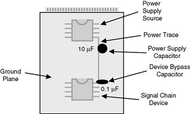
Figure 38.1 In analog and digital PCB design, you should place the bypass or decouple capacitors (0.1 μF) as close to the device as possible. You should also place the power supply decoupling-capacitor (10 μF) at the power-source or where the power-bus enters the board. In all cases, these capacitors should have short leads.
The placements of the bypass or decoupling capacitors are just common sense for both types of designs, but interesting enough, for different reasons. In the analog layout design, bypass capacitors generally serve the purpose of redirecting high frequency signals on the power supply trace. This noise would otherwise enter into the sensitive analog chip, through the power supply pin. Generally, these high frequency signals occur at frequencies beyond rejection capability of the analog device. The possible consequences of not using a bypass capacitor in your analog circuit are the addition of undue noise to the signal path or worse yet, oscillation.
For digital devices, such as controllers and processors, the decoupling capacitor on the power supply pin are required, but for a different reason. One of the functions of these capacitors is to serve as a “mini” charge reservoir. Frequently in digital circuits, a great deal of current is required to execute the transitions of the changing gate states.Because of the switching transient currents that occur on the chip and throughout the circuit board, having additional charge “on-call” is advantageous. The consequence of not having enough charge locally to execute this switching action could result in a significant dynamic and static change in the power supply voltage. When the voltage change is too large, it will cause the digital signal level to go into the indeterminate state. But more than likely, the state machines in the digital device will operate erroneously. The switching current passing through the circuit board traces causes this change in voltage. The circuit board traces have parasitic inductance. You can calculate the change in voltage results with this formula:
![]()
where, V = voltage change
So for multiple reasons, it is a good idea to bypass (or decouple) the power supply at the power supply and at the power supply pin of all of the active devices.
38.1.2 The Power and Ground Should Be Routed Together
When you match power and ground traces with respect to location, you lessen the opportunities for EMI. If you don’t match power and ground, system loops are part of the layout. The possibility of seeing “noisy” results without explanation is real. Figure 38.2 shows an example of a PCB design with the unmatched power and ground traces.

Figure 38.2 The power and ground traces are laid out using different routes to the device on this board. This mismatch opens the opportunity for EMI into the electronics of this board.
The loop area in Figure 38.2 is 697 cm2. This loop is a perfect antenna for noise in the area. With this board, you may be able to pick up radio signals. In the 1980s, one of the German engineers that I worked with was able to design boards of this class and “pick-up” Radio Free Europe.
Figure 38.3 shows a dramatic decrease in radiated noise off the board for induced voltages in the loop. This is because there is a decrease of radiated noise off the board and around the board.

Figure 38.3 In this one-layer board, the power trace and ground trace are laid next to each other on their way to the device on this board. Figure 38.2 shows a board where the traces are better matched. The opportunity for EMI into the electronics of this board is lessened by 679/12.8 or ∼54×.
In Figure 38.3, the signal and ground line are next to each other. This greatly reduces the loop area. A better solution would be to have a ground plane, which would be underneath the power supply trace. An even better solution would be to have a ground plane and a separate power plane.
38.2 Where the Domains Differ—Ground Planes Can Be a Problem
The fundamentals of circuit board layout apply to analog circuits as well as digital circuits. One fundamental rule of thumb is to use uninterrupted ground planes. This common practice reduces the effects of δI/δt (change in current with time) in digital circuits. In digital circuits, the change in current with time changes the potential of ground. In analog circuits, injected noise is caused by δI/δt. But, when comparing digital and analog circuits, you should exercise an added precaution with analog circuits in order to keep the digital signal lines and return paths in the ground plane as far away from the analog circuitry as possible. This can be done by connecting the analog ground plane separately to the system ground connect or having the analog circuitry at the farthest side of the board—that is, at the end of the line. This is done so that signal paths have a minimal amount of interference from external sources. The opposite is not true for digital circuitry. The digital circuitry can tolerate a great deal of noise on the ground plane before problems start to appear.
38.2.1 Location of Components
In every PCB design, you should separate the noisy and quiet portions of the circuit, as mentioned above. Generally, the digital circuitry is “rich” with noise. Alternatively, digital circuitry is less sensitive to this type of noise because of the larger voltage noise margins. When you look at analog circuits, you will easily find that they are not as forgiving as the digital circuits. The voltage noise margins of the analog circuitry are much smaller. Of the two domains, the analog domain is most sensitive to switching noise. In the layout of a mixed-signal system, you should separate the two domains. Figure 38.4 shows this graphically.

Figure 38.4 If possible, (A) the digital and analog portion of circuits should be separated in order to separate the digital switching activity from the analog circuitry. Additionally, (B) the high frequency should be separated from the low frequency where possible, keeping the higher frequency components closer to the board connector.
The general rules of thumb are to keep the analog and digital portions of the circuit separate, with the digital circuitry closest to the connector. This is done so that the fast changing digital signals never “go past” the analog chips. A second general guideline is to place the higher frequency devices closer to the connector than the lower frequency devices. In this case, higher frequency noise will not inject into the lower frequency devices.
38.3 Where the Board and Component Parasitics Can Do the Most Damage
The major classes of parasitics generated by the PC board layout come in the form of resistors, capacitors, and inductors. For instance, you can build PCB resistors with your traces that span between components. You can build unintentional capacitors into the board with traces, soldering pads, and parallel traces. Unintentional inductors come from loop inductance, mutual inductance, and vias. All of these parasitics stand a chance of interfering with the effectiveness of your circuit as you transition from the circuit diagram to the actual PCB. You will clearly see in this section of the chapter the most troublesome class of board parasitics and see examples of where these parasitics have the most effect on circuit performance.
38.3.1 Feeling the Pain of Those Unnecessary Capacitors
You can design a capacitor into a board by simply placing two traces close to each other. This can be done by placing the two traces one on top of the other with two layers (which is harder to see) or by placing them beside each other on the same layer. Usually, you would build layout capacitors by placing two parallel traces close together. The formulas in Figure 38.5 show how you can calculate the value of this type of capacitor.

Figure 38.5 You can easily place capacitors into a PCB by laying out two traces in close proximity. With this type of capacitor, fast voltage changes on one trace can initiate a current signal in the other trace.
In both trace configurations, changes in voltage with time (δV/δt) on one trace could generate a current on a second trace. If the second trace is high impedance, the e-field creates current, which converts to voltage. Typically, you will find fast voltage transients on the digital side of the mixed signal design. If the traces that have these fast, voltage transients are in close proximity to high impedance, analog traces, this type of error will be very disruptive with analog circuitry accuracy. Analog circuitry has two strikes against it in this environment. The noise margins are much lower than digital and it is not unusual to have high impedance traces.
You can easily minimize this type of phenomena using one of two techniques. The most commonly used technique is to change the dimensions between the traces, as the capacitor equation suggests. The most effect dimension to change is the distance between the two offending traces. It should be noted that the variable, d, is in the denominator of the capacitor equation. As d is increased, the capacitance will decrease. The length of the two traces is another variable that you can change. In this case, if you reduce the length (L), this also reduces the capacitance between the two traces.
Another technique used is to lay a ground trace between the two offending traces. Not only is the ground trace low impedance, but an additional trace like this will break up the E-fields that are causing the disturbance.
This type of capacitor can cause problems in mixed signal circuits where sensitive, high impedance, analog traces are in close proximity to digital traces. For example, the circuit in Figure 38.6 has the potential to have this type of problem.

Figure 38.6 You can build a 16-bit DAC using three 8-bit digital potentiometers and three amplifiers to provide 65,536 different output voltages. If VDD is 5V in this system the resolution or LSB size of this DAC is 76.3 μV.
To quickly explain the circuit operation in Figure 38.6, a 16-bit DAC uses three 8-bit digital potentiometers and three CMOS operational amplifiers. To the left side of this figure, two digital potentiometers (U3a and U3b) span across VDD to ground with the wiper output connected to the noninverting input of two amplifiers (U4a and U4b). You program the digital potentiometers, U2 and U3 by using an SPI interface between the microcontroller, U1. In this configuration, each digital potentiometer operates as an 8-bit multiplying DAC. If VDD is equal to 5V, the LSB size of these DACs is equal to 19.61 mV.
In this circuit, you connect the wipers digital potentiometers (U4a, U4b) to the noninverting inputs of two buffer amplifiers. In this configuration, the inputs to the amplifiers are high impedance, which isolates the digital potentiometers from the rest of the circuit. The output swing restrictions of the second stage of this amplifier configuration are not violated.
To have this circuit perform as a 16-bit DAC (U2a), a third digital potentiometer spans across the output of these two amplifiers, U4a, and U4b. The programmed setting of U3a and U3b sets the voltage across the digital potentiometer. Again, if VDD is 5V it is possible to program the output of U3a and U3b 19.61 mV apart. With this size of voltage across the third 8-bit digital potentiometer (R3), the LSB size of this circuit from left to right is 76.3 μV. Table 38.1 shows the critical device specifications that give optimum performance with this circuit.
Table 38.1 From the long list of specifications that each of the devices have, there are a handful of key specifications that make this circuit more successful when it is used to provide DC reference voltages or arbitrary wave forms

You can use this circuit in two basic modes of operation. The first mode would be if you wanted a programmable, adjustable, DC reference. In this mode, you only use the digital portion of the circuit occasionally and certainly not during normal operation. The second mode would be if you used the circuit as an arbitrary wave generator. In this mode, the digital portion of the circuit is an intimate part of the circuit operation. In this mode, the risk of capacitive coupling may occur.
Figure 38.7 shows the first pass layout of the circuit. You can quickly design this circuit in your lab without attention to detail. The consequences of placing digital traces next to high impedance, analog lines were overlooked in the layout review. This speaks strongly to doing it right the first time, but to your benefit, I made this mistake and you can see how I made significant improvements.
Figure 38.7 This is the first attempt at the layout for the circuit in Figure 38.6. In this figure, you can see that a critical, high impedance, analog line is very close to a digital trace. This configuration produces inconsistent noise on the analog line because the data input code on that particular digital trace changes. These changes are dependent on the programming requirements for the digital potentiometer.
If you take a look at this layout, it is obvious where a potential problem is. The arrow is pointing to an analog trace. This trace is from the wiper of U3a to the high impedance amplifier input of U4a. The digital trace that is pointed out carries the digital word that programs the digital potentiometer settings.
On the bench, I measured the digital signal that was coupled into the sensitive analog wiper trace. Figure 38.8 shows the scope photo.
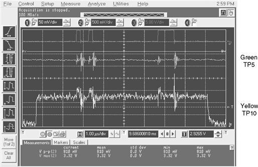
Figure 38.8 In this scope photo, the top trace was taken at JP1 (digital word to the digital potentiometers), the second trace on JP5 (noise on the adjacent analog trace), and the bottom yellow trace is taken at TP10 (noise at the output of the 16-bit DAC).
The digital signal that is programming the digital potentiometers in the system has transmitted from trace to trace onto an analog line that is being held at a DC voltage. This noise propagates through the analog portion of the circuit all the way out to the third digital potentiometer (U5a). The third digital potentiometer is toggling between two output states.
What is the solution to this problem? Basically, you should separate the traces. Figure 38.9 shows an improved layout solution.

Figure 38.9 With a new layout, the analog lines are separate from the digital lines. This distance has eliminated the digital noise that was causing interference in the previous layout.
Figure 38.10 shows the results of the layout change. With the analog and digital traces carefully kept apart, this circuit becomes a very clean 16-bit DAC. This trace shows a single code transition of the third digital potentiometer of 76.29 μV. You may notice that the oscilloscope scale is 80 mV/div and that the amplitude of this code change is approximately 80 mV. In the lab, the equipment forced us to gain the output of the 16-bit DAC by 1000×.
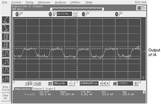
Figure 38.10 The 16-bit DAC in this new layout is showing a single code transition with no digital noise from the communication to the digital potentiometers
Once again, when the digital and analog domains meet, careful layout is critical if you intend to have a successful final PCB implementation. In particular, active digital traces close to high impedance analog traces will cause serious coupling noise. You can avoid this noise coupling phenomena by putting distance between traces.
38.3.2 Inductors Designed into the PCB
The way that an inductor is designed into a board is similar to the construction of a capacitor. Again this is done by placing two traces, one on top of the other with two layers or by placing them beside each other on the same layer, as shown in Figure 38.11. In both trace configurations, changes in current with time (δI/δt) on one trace could generate a voltage in the same trace due to the inductance on that trace and initiate a proportional current on the second trace due to the mutual inductance. If the voltage change is high enough on the primary trace, the disturbance can reduce the voltage margin of the digital circuitry enough to cause errors. This phenomenon is not necessarily reserved for digital circuits, but is more common in that environment because of the larger, seemingly instantaneous switching currents.

Figure 38.11 If you pay little attention to the placement of traces, you can create line and mutual inductance with the traces in a PCB. This kind of parasitic element is most detrimental to the circuit operation where digital switching circuits reside.
To eliminate potential noise for EMI sources it is best to separate quiet analog lines versus noisy I/O ports. Try to implement low impedance power and ground networks, minimize inductance in conductors for digital circuits and minimize capacitive coupling in analog circuits.
38.4 Layout Techniques That Improve ADC Accuracy and Resolution
Initially, analog-to-digital (A/D) converters arose from an analog paradigm where a large percentage of the physical silicon was analog. As the progression of new design topologies evolves, this paradigm is shifting to where slower speed A/D converters are predominantly digital. Even with this on-chip shift from analog to digital, the PCB layout practices have not changed. Now as always, when the layout designer is working with mixed-signal circuits, you still need key layout knowledge in order to implement an effective layout. This section of the chapter will look at the PCB layout strategies required for A/D converters using successive approximation register (SAR) and sigma-delta topologies.
38.4.1 SAR Converter Layout
SAR A/D converters can be found with 8-bit, 10-bit, 12-bit, 16-bit and sometimes 18-bit resolution. Originally, the process and architecture for these converters was bipolar with R-2R ladders. But recently these devices have migrated to a CMOS process with a capacitive charge distribution topology. Needless to say, the system layout strategy for these converters has not changed with this migration. The basic approach to layout is consistent, except for higher resolution devices. These devices require more attention to the prevention of digital feedback from the serial or parallel output interface of the converter.
The SAR converter is predominantly analog in terms of circuitry and the amount of real estate dedicated to the different domains on the chip. Figure 38.12 shows a block diagram of a 12-bit, CMOS SAR converter.

Figure 38.12 This is a block diagram of a 12-bit CMOS SAR A/D converter. This converter uses a charge distribution across a capacitive array
These types of converters can have several pins for the ground and power connections. The pin names are often misleading in that you cannot differentiate between the analog and digital connections with the pin label. These labels do not necessarily describe the system connections to the PCB, but rather they identify how the digital and analog currents come off the chip. Knowing this information and understanding that the primary real estate consumed on the SAR converter chip is analog, it makes sense to connect the power and ground pins on the same planes. And since the converter is primarily an analog chip, placing the pins of the device on the analog planes is very appropriate.
Figure 38.13 shows the pinout for a representative sample of 10-bit and 12-bit converters.

Figure 38.13 The SAR converter, regardless of resolution, usually has at least two ground connects; AGND (VSS) and DGND (VSS). The converters illustrated here are the MCP3008 and MCP3201 from Microchip.
With these devices, the ground signal is usually directed off the chip with two pins; AGND and DGND. The power is applied to a single pin. When implementing the PCB layout, you should connect AGND and DGND to the analog ground plane. The analog and digital power pins should also be connected to the analog power plane or at least connected to the analog power train with proper bypass capacitors as close to each pin as possible. The only reason that these devices would have only one ground pin and one positive supply pin is due to package pin limitations. However, separate grounds on the chip enhance the probability of getting good and repeatable accuracy from the converter.
With all of the converters, the power supply strategy should be to connect all grounds, positive supply and negative supply pins to the analog planes. In addition, you should connect the COM pin or IN- pin associated with the input signal as close to the signal ground as possible.
Higher resolution SAR converters (16- and 18-bit converters) require a little more consideration in terms of separating the digital noise from the quiet analog converter and power planes. When you interface these devices to a microcontroller, external digital buffers should be used in order to achieve clean operation. Although, these types of SAR converters typically have internal double buffers at the digital output, you can use external buffers to further isolate the digital bus noise from the analog circuitry in the converter. Figure 38.14 shows an appropriate power strategy for this type of system.

Figure 38.14 With high-resolution SAR A/D converters, you should connect the analog planes to the converter power and ground. You should then buffer the digital output of the A/D converter by using external 3-state output buffers. These buffers provide isolation between the analog and digital side, as well as high-drive capability.
38.4.2 Precision Sigma-Delta Layout Strategies
The silicon area of the precision sigma-delta A/D converter is predominantly digital. In the early days, when this type of converter was first being produced, this shift in the paradigm prompted users to separate the digital noise from the analog noise by using the PCB planes. As with the SAR A/D converter, these types of A/D converters can have multiple analog-and digital-ground and power pins. Once again, the common tendency of a digital or analog design engineer is to try separating these pins into separate planes. Unfortunately, this is a misguided tendency, particularly if you intend to solve critical noise problems with the 16-bit to 24-bit accuracy devices.
With a high-resolution sigma-delta converter that has a 10-Hz data rate, the clock (internal or external) to the converter could be as high as 10 MHz or 20 MHz. You would use this high frequency clock for switching the modulator and running the oversampling engine. With these circuits, you should connect the AGND and DGND pins together on the same ground plane, as is the case with the SAR converter. Additionally, you should connect the analog and digital power pins together, preferably on the same plane. The requirements on the analog and digital power planes are the same as with the high-resolution SAR converters.
A ground plane is mandatory, which implies that at a minimum you need a two-layer board. On this double-sided board, the ground plane should cover at least 75% of the area if not more. You should keep interruptions in the plane to an absolute minimum. The purpose of this ground plane layer is to reduce grounding resistance and inductance as well as provide a shield against electro-magnetic interference (EMI) and radio-frequency interference (RFI). If the circuit, interconnect traces need to be on the ground-plane side of the board, they should be as short as possible and perpendicular to the ground current return paths.
You can get away without separating the analog and digital pins of low precision A/D converters, such as 6-, 8-, or maybe even 10-bit converters. But as the resolution/accuracy increases with your converter selection, the layout requirements also become more stringent. In both cases, with high-resolution SAR A/D converters and sigma-delta converters you need to connect them directly to the lower noise, analog ground and power planes.
38.5 The Art of Laying Out Two-Layer Boards
In this highly competitive marketplace, the cost objective usually dictates that a designer use two-layer boards in the design. Although the multi-layer board (4-, 6-, and 8-layers) allows the designer to build cleaner solutions in terms of size, noise, and performance, financial pressures force the engineer to rethink layout strategies with the two-layer board in mind. In this section of this chapter we will discuss the use or misuse of auto routing, the concept of current return paths with and without ground planes, and recommendations for component placement where two layer boards are concerned.
38.5.1 Pay Now or Pay Later with the Auto Router and Analog Circuits
It is tempting to use the auto router when designing printed circuit board (PCB). More often than not, a purely digital board (especially if the signals are relatively slow, and the circuit density is low) will work just fine. But as you try to lay out analog, mixed signal or high-speed circuits with the auto routing tool that is available with your layout software, there may be some issues. The probability of creating serious circuit performance problems is very high.
Figure 38.15 shows the auto routed top layer of a two-layer board. The bottom layer of this board is in Figure 38.15 and 38.16 and the circuit diagram for these layout layers is in Figure 38.17 and Figure 38.18.

Figure 38.15 Top layer of an auto-routed layout of circuit diagram shown in Figure 38.17 and Figure 38.18

Figure 38.16 Bottom layer of an auto-routed layout of circuit diagram shown in Figure 38.17 and Figure 38.18

Figure 38.17 Digital section of circuit diagram for layouts in Figures 38.15, 38.16, 38.19, and 38.20. This is the circuit diagram from Microchip’s MXDEV™ board, evaluation board for the 10- and 12-bit ADCs (MCP300X and MCP320x).

Figure 38.18 Analog section of circuit diagram for layouts in Figures 38.15, 38.16, 38.19, and 38.20. This is the circuit diagram from Microchip’s MXDEV board, evaluation board for the 10- and 12-bit ADCs (MCP300X and MCP320x).
With this layout, there are several areas of concern, but the most troubling issue is the grounding strategy. If you follow the ground traces on the top layer, the traces connect every device on that layer. A second ground connection for every device uses the bottom layer with vias at the far right-hand side of the board. The immediate red flag that one should see when examining this layout strategy would be the existence of several ground loops. Additionally, horizontal signal lines interrupt the ground return paths on the bottom side. The saving grace with this grounding scheme is that the analog devices (12-bit A/D converter and 2.5V voltage reference) are at the far right-hand side of the board. This placement ensures that digital ground signals do not pass under these analog chips.
Figure 38.19 and Figure 38.20 have the manual layouts of the circuits in Figure 38.17 and Figure 38.18. For the layout of this mixed-signal circuit, the devices were manually placed on the board with careful thought to separating the digital and analog devices. With this manual layout, a few general guidelines are followed to ensure positive results. These guidelines are:
1. Use the ground plane as a current return path as much as possible.
2. Separate the analog ground plane from the digital ground plane with a break.
3. If interruptions from signal traces are required on the ground-plane side, make them vertical to reduce the interference with the ground-current, return paths.
4. Place analog circuitry at the far end of the board and digital circuitry closest to the power connects. This reduces the effects of δi/δt from digital switching.

Figure 38.19 Top layer of a manual routed layout of circuit diagram shown in Figure 38.17 and Figure 38.18

Figure 38.20 Bottom layer of a manual routed layout of the circuit diagram shown in Figure 38.17 and Figure 38.18
Note that with both of these two layer boards there is a ground plane on the bottom. This is only done so that an engineer working on the board can quickly see the layout when troubleshooting. You will typically find this strategy in manufacturer’s demo and evaluation boards.
But more typically, the ground plane is on the top of board, thereby reducing electromagnetic interference (EMI).
At every layout-related presentation that I give in a seminar setting, the question always asked in one form or another is, “What if management tells me I can’t have two layers or a ground plane, and I still need to reduce noise in the circuit? How do I design my circuit to work around the need for a ground plane?” Typically, I instruct the person asking the question to inform their management that a ground plane is simply required if they want reliable circuit performance. The primary reason for using ground planes is lower ground impedance. They also provide a degree of EMI reduction.
38.6 Current Return Paths With or Without a Ground Plane
The fundamental issues that should be considered when dealing with current return paths are:
1. If traces are used, they should be as wide as possible.
In the event that you are considering using traces for your ground connects on your PCB, they should be as wide as possible. This is a good rule of thumb, but also understand that the thinnest width in your ground trace will be the effective width of the trace from that point to the end (where the “end” is defined as the point furthest from the power connection).
2. You should avoid ground loops.
3. If no ground plane is available, you should use a star connection strategy.
Figure 38.21 shows a graphical example of a star connection strategy.
With this type of approach, the ground currents return to the power connection independently. You will note that in Figure 38.21 not all of the devices have their own return path. With U1 and U2, the return path is shared. This can be done if you use guidelines #4 and #5, following.

Figure 38.21 If a ground plane is not feasible, you should handle current return paths with a “star” layout strategy
4. Digital currents should not pass across analog devices.
During switching, digital currents in the return path are fairly large, but only briefly. This phenomenon occurs due to the effective inductance and resistance of the ground. With the inductance portion of the ground plane or trace, the governing formula is V = Lδi/δt, where V is the resulting voltage, L is the inductance of the ground plane or trace, δi is the change in current from the digital device and δt is the time span considered for the event. To calculate the effects of the resistance portion of the ground plane, changes in the voltage simply change because of V = RI. Again, V is the resulting voltage, R is the ground plane or trace resistance and I is the current change caused by the digital device. These changes in the voltage of the ground plane or trace across the analog device will change the relationship between ground and the signal in the signal chain.
5. High-speed current should not pass across lower speed devices.
Ground-return signals of high-speed circuits have a similar effect on changes to the ground plane. Again the more important formulas that determine the effects of this interference are V = Lδi/δt for the ground plane or trace inductance and V = RI for the ground plane or trace resistance. And as with digital currents, high-speed circuits that have ground activity on the ground plane or that have a trace across the analog device change the relationship between ground and the signal in the signal chain.
6. Regardless of the technique used, you must design the ground return paths to have a minimum resistance and inductance.
7. If a ground plane is used, breaks in plane can improve or degrade circuit performance. Use with care.
But, if you are unable to win that battle with your management because of cost constraints, this book offers some suggestions. These suggestions are using star networks and current return paths, which if used properly, will give a little relief from the circuit noise.
38.7 Layout Tricks for a 12-bit Sensing System
When I started writing this chapter I thought a “cookbook” approach would be appropriate when describing the implementation of a good 12-bit layout. My assumption behind this type of approach is that I would provide a reference design, which would make the layout implementation easy. But I struggled with this topic long enough to find that this notion was fairly unrealistic.
Because of the complexity of this problem, I am going to provide basic guidelines ending with a review of issues to be aware of while implementing your layout design. Throughout this discussion I will offer examples of good and bad layout implementations. I am doing this in the spirit of discussing concepts and not with the intent of recommending one layout as the only one to use.
The application circuit that I’m going to use is a load-cell circuit that accurately measures the weight applied to the sensor, then displays the results on a LCD-display screen. Figure 38.22 shows the circuit diagram for this system. You can purchase the load cell that I used from Omega (LCL-816G). My sensor model for the LCL-816G is a four element resistive bridge that requires voltage excitation. With a 5V excitation voltage applied to the high side of the sensor, the full-scale output swing is a ±10 mV differential-signal with a 32-ounce maximum excitation. A two-op-amp instrumentation amplifier gains this small differential signal. I chose a 12-bit converter to match the required precision of this circuit. Once the converter digitizes the voltage presented at its input, the microcontroller receives the digital code by using the converter’s SPI™ port. The microcontroller then uses a look-up table to convert the digital signal from the ADC into weight. Linearization and calibration activities can be implemented with controller code at this point if need be. Once this is done, the results are sent to the LCD display. As a final step, I wrote the firmware for the controller. Now the design is ready to go to board layout.
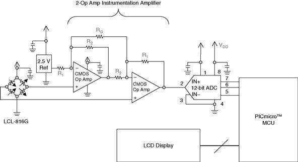
Figure 38.22 A two-op-amp instrumentation amplifier, filtered and digitized with a 12-bit A/D converter, gains the signal at the output of the load-cell sensor. The result of each conversion is sent to the LCD display.
38.8 General Layout Guidelines—Device Placement
My first step is to place the devices on the board. This critical step is done effectively because I am keeping track of my noise-sensitive devices and noise-creator devices. There are two guidelines that I use to accomplish this task:
1. Separate the circuit devices into two categories: high speed (>40 MHz) and low speed. You should place the higher speed devices closer to the board connector/power supply.
2. Separate the above categories into three subcategories: pure digital, pure analog, and mixed signal. With this delineation, you need to place the digital devices closer to the board connector/power supply.
38.9 General Layout Guidelines—Ground and Power Supply Strategy
Once I determine the general location of the devices, I was able to define my ground and power planes. My strategy of the implementation for these planes is a bit tricky.
First of all, it is dangerous for me not to use a ground plane in a PCB implementation. This is true particularly in analog and/or mixed-signal designs. One issue is that ground noise problems are more difficult to deal with than power-supply noise problems because analog signals are referenced to ground. For instance, in the circuit shown in Figure 38.22, the A/D converter’s inverting input pin (MCP3201, Microchip) is connected to ground. Secondly, the ground plane also serves as a shield against emitted noise. Both of these problems are easy to resolve with a ground plane and nearly impossible to overcome if there is no ground plane.
However, with my small design, I assume that I won’t need a ground plane. Figure 38.23 shows a ground plane-less, layout implementation of the circuit in Figure 38.22.

Figure 38.23 This is the layout of the top (A) and bottom (B) layers of the circuit in Figure 38.22. Note that this layout does not have a ground or power plane. Note that the power traces are considerably wider than the signal traces in order to reduce power supply trace inductance.
Does my “no ground plane is required” theory play out? The proof is in the pudding, or data. In Figure 38.24, 4096 samples were taken from the A/D converter and logged. There was no excitation on the sensor when this data was taken. With this circuit layout, the controller is dedicated to interfacing with the converter and sending the converter’s results to the LCD display.

Figure 38.24 This is a histogram of 4096 samples from the output of the A/D converter. The PCB does not have a ground or power plane as shown in the PCB layout in Figure 38.25. The code of the noise from the circuit is 15 codes wide (Figure 38.23).
Figure 38.25 shows the same device layout shown in Figure 38.23, but a ground plane on the bottom layer is added. The ground plane (Figure 38.25B) has a few breaks due to signal. These breaks should be kept to a minimum. Current return paths should not be “pinched” as a consequence of these traces restricting the easy flow of current from the device to the power connector. Figure 38.26 shows the histogram for the A/D converter output. Compared to Figure 38.24, the output codes are much tighter. The same active devices were used for both tests. The passive devices were different causing a slight offset difference.
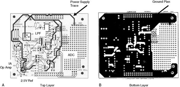
Figure 38.25 This is the layout of the top and bottom layers of the circuit in Figure 38.22. Note that this layout does have a ground plane.
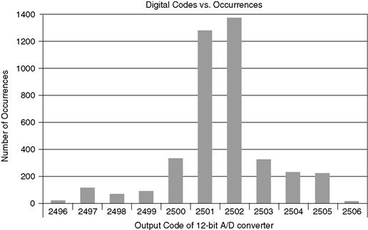
Figure 38.26 This is a histogram of 4096 samples from the output of the A/D converter on the PCB that has a ground plane as shown in the PCB layout in Figure 38.25. The code width of the noise is now 11 codes wide.
It is clear from my data that a ground plane does have an effect on the circuit noise. When my circuit did not have a ground plane, the width of the noise was ∼15 codes. When I added a ground plane, I improved the performance by almost 1.5× or 15/11. You might want to know that my test set-up was in the lab, where EMI interference is relatively low.
The op-amp and absence of an anti-aliasing filter are causes of the noise shown in Figure 38.26. If my circuit has a minimum amount of digital circuitry on board, a single ground plane and a single power plane may be appropriate. The board designer defines my qualifier minimum. The danger of connecting the digital and analog ground planes together is that my analog circuits can pick up the noise on the supply pins and couple it into the signal path. In either case, I should connect my analog and digital grounds and power supplies together at one or more points in the circuit. This ensures that my power supply, input, and output ratings of all of the devices are not violated.
The inclusion of a power plane in a 12-bit system is not as critical as the required ground plane. Although a power plane can solve many problems, making the power traces two or three times wider than other traces on the board and by using bypass capacitors effectively can reduce power noise.
38.10 Signal Traces
My signal traces on the board (both digital and analog) should be as short as possible. This basic guideline will minimize the opportunities for extraneous signals to couple into the signal path. One area to be particularly cautious of is with the input terminals of analog devices. These terminals normally have a higher impedance than the output or power supply pins. As an example, the voltage reference input pin to the A/D converter is most sensitive while a conversion is occurring. With the type of 12-bit converter I have in Figure 38.22, my input terminals (IN+ and IN–) are also sensitive to injected noise. Another potential for noise injection into my signal path is the input terminals of an operational amplifier. These terminals have typically 109 Ω to 1013 Ω input impedance.
My high impedance input terminals are sensitive to injected currents. This can occur if the trace from a high impedance input is next to a trace that has fast changing voltages, such as a digital or clock signal. When a high impedance trace is in close proximity to a trace with these types of voltage changes, charge is capacitively coupled into the high impedance trace as mentioned earlier in the chapter.
38.11 Did I Say Bypass and Use an Anti-Aliasing Filter?
Although this chapter is about layout practices, I thought it would be a good idea to cover some of the basics in circuit design. A good rule concerning bypass capacitors is to always include them in the circuit. If they are not included, the power supply noise may very well eliminate any chance for 12-bit precision.
38.12 Bypass Capacitors
Bypass capacitors belong in two locations on the board: one at the power supply (10 μF to 100 μF or both) and one for every active device (digital and analog). The value of the bypass capacitor of the device is dependent on the device in question. If the bandwidth of the device is less than or equal to ∼1 MHz, a 1 μF will reduce injected noise dramatically. If the bandwidth of the device is above ∼10 MHz, a 0.1 μF capacitor is probably appropriate. In between these two frequencies, you could use both or either one. Refer to the manufacturer’s guidelines for specifics.
Every active device on the board requires a bypass capacitor. It must be placed as close as possible to the power supply pin of the device as shown in Figure 38.25. If you use two bypass capacitors for one device, the smaller one should be closest to the device pin. Finally, the lead length of the bypass capacitor should be as short as possible.
38.13 Anti-Aliasing Filters
You will note that the circuit in Figure 38.22 does not have an anti-aliasing filter. As the data shows, this oversight has caused noise problems in the circuit. When this board has a second order, 10 Hz, anti-aliasing filter inserted between the output of the instrumentation amplifier and the input of the A/D converter, the conversion response improves dramatically. Figure 38.27 shows the resulting data.
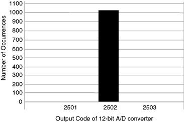
Figure 38.27 This diagram shows the conversion results of the circuit in Figure 38.22 plus a second order, anti-aliasing filter. Additionally, the board layout includes a ground plane.
Analog filtering can remove noise superimposed on the analog signal before it reaches the A/D converter. In particular, this includes extraneous noise peaks. Analog-to-digital converters will convert the signal that is present on its input. This signal could include the sensor voltage signal or noise. The anti-aliasing filter removes the higher frequency noise from the conversion process.
38.14 PCB Design Checklist
Good layout techniques are not difficult to master as long as you follow a few guidelines:
1. Check device placement versus connectors. Make sure that high-speed devices and digital devices are closest to the connector.
2. Always have at least one ground plane in the circuit.
3. Make power traces wider than other traces on the board.
4. Review current return paths and look for possible noise sources on ground connects. Determining the current density at all points of the ground plane and the amount of possible noise present does this.
5. Bypass all devices properly. Place the capacitors as close to the power pins of the device as possible.
6. Keep all traces as short as possible.
7. Follow all high impedance traces looking for possible capacitive coupling problems from trace to trace.
8. Make sure you properly filter your signals in a mixed-signal circuit.
Analog layout and digital layout techniques differ slightly, but not completely. When it comes to the parasitic components embedded in the PCB, the analog circuits tend to show more sensitivity, but digital circuits are not completely immune. You should treat the device that straddles these two domains, such as the A/D converter, as an analog device. Two-layer boards do present some challenges, but careful manual layouts can usually work around these problems. You can fix a poor layout if you are willing to go back to the drawing board.
When the analog and digital domains meet, careful layout is critical if a designer intends to have a successful final PCB implementation. Layout strategies usually are presented as rules of thumb because it is difficult to test the success of your final product in a lab environment. So, generally speaking, although there are some similarities in layout strategies between the digital and analog domain, the differences should be recognized and worked with.
Solving signal integrity problems can take a great deal of time, particularly if you don’t have the tools to tackle the tough issues. The three best analysis tools to have in your arsenal are the frequency analysis (fast Fourier transform or FFT), time analysis (scope photo), and DC analysis (histogram) tools. We used all of these tools to identify the power supply noise, external clock noise, and overdriven amplifier distortion.
References
1. MXDEV is a trademark of Microchip Technology Inc. in the USA and other countries.
2. SPI™ port is a trademark of Motorola. The Microchip name and logo, PIC, PICmicro, microID and KEELOQ are registered trademarks of Microchip Technology Inc. in the USA and other countries. All other trademarks are the property of their respective owners.
3. Ott Henry W, ed. Noise Reduction Techniques in Electronic Systems. Wiley 1998.
4. Morrison Ralph. Noise and Other Interfering Signals John Wiley & Sons 1992.
5. Baker Bonnie C. Circuit Layout Techniques and Tips: 6 Part analogZone 2002.