
Chapter 11
Sequential Logic Design
11.1 Introduction
Sequential logic circuits are based on combinational logic circuit elements (AND, OR, etc.) working alongside sequential circuit elements (latches and flip-flops). A generic sequential logic circuit is shown in Figure 11.1. Here, the circuit inputs are applied to and the circuit outputs are derived from a combinational logic block. The sequential logic circuit elements store an output from the combinational logic that is fed back to the combinational logic input to constitute the present state of the circuit. The output from the combinational logic that forms the inputs to the sequential logic circuit elements constitutes the next state of the circuit. These sequential logic circuit elements are grouped together to form registers. The circuit changes state from the present state to the next state on a clock control input (as happens in a synchronous sequential logic circuit). Commonly, the D-latch and D-type flip-flops are used (rather than other forms of latch and flip-flop such as the S-R, toggle, and J-K flip-flops), and they will be discussed in this text. The output from the circuit is taken from the output of the combinational logic circuit block.

Figure 11.1 Generic sequential logic circuit (counter or state machine)
In general, sequential logic circuits may be asynchronous or synchronous:
1. Asynchronous sequential logic. This form of sequential logic does not use a clock input signal to control the timing of the circuit. It allows very fast operation of the sequential logic, but its operation is prone to timing problems where unequal delays in the logic gates can cause the circuit to operate incorrectly.
2. Synchronous sequential logic. This form of sequential logic uses a clock input signal to control the timing of the circuit. The timing of changes in states in the sequential logic is designed to occur either on the edge of the clock input when flip-flops are used, or at a particular logic level, as when latches are used. State changes that occur on the edge of the clock input, as when flip-flops are used, occur either on a 0 to 1 rise, referred to as positive edge triggered, or on a 1 to 0 fall, referred to as negative edge triggered.
In this text, only synchronous sequential logic will be considered.
An alternative view for the generic sequential logic circuit in Figure 11.1, is shown in Figure 11.2. Here, the combinational logic is separated into input and output logic. Both views are commonly used in the description of sequential logic circuits.
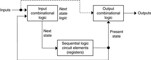
Figure 11.2 Alternative view for the generic sequential logic circuit
In designing the synchronous sequential logic circuit (from now on simply referred to as the sequential logic circuit), the designer must consider both the type of sequential logic circuit elements (latch or flip-flop) and the combinational logic gates. The design uses the techniques previously discussed—Boolean logic expressions, truth tables, schematics, and Karnaugh maps—to determine the required input combinational logic (the next state logic) and determine the required output combinational logic.
The sequential logic circuit will form one of two types of machines:
1. In the Moore machine, the outputs are a function only of the present state only.
2. In the Mealy machine, the outputs are a function of the present state and the current inputs.
In addition, the sequential logic circuit will be designed either to react to an input or to be autonomous. In an autonomous sequential logic circuit, there are no inputs (apart from the clock and reset/set) to control the operation of the circuit, so the circuit moves through states under the control of only the clock input. An example of an autonomous sequential logic circuit is a straight binary up-counter that moves through a binary count sequence taking the outputs directly from the sequential logic circuit element outputs. A sequential logic circuit can also be designed to react to an input: a sequential logic circuit that reacts to an input is called a state machine in this text.
Sequential logic circuit design follows a set design sequence aided by:
• state transition diagram, which provides a graphical means to view the states and the transitions between states; and
• state transition table, similar in appearance to a combinational logic truth table, which identifies the current state outputs and the possible next state inputs to the sequential logic circuit elements.
As an example, consider a circuit that is to detect the sequence 1001 on a serial bitstream data input and produce a logic 1 output when the sequence has been detected, as shown in Figure 11.3. The state machine will have three inputs—one Data_In that is to be monitored for the sequence and two control inputs, Clock and Reset—and one output, Detected. Such a state machine could be used in a digital combinational lock circuit.

Figure 11.3 1001 sequence detector
An example state transition diagram for this design is shown in Figure 11.4. The circuit is to be designed to start in State 0 and has five possible states. With these five states, if D-type flip-flops are to be used, then there will need to be a need for three flip-flops (producing eight possible states although only five will be used when each state is to be represented by one value of a straight binary count sequence 0, 1, 2, 3, 4, 0, etc.). The arrangement for the state transition diagram is:
1. The circles identify the states. The name of the state (the state identifier) and the outputs for each state are placed within the circle. Each state is referred to as a node.
2. The transition between states uses a line with the arrow end identifying the direction of movement. Each line starts and ends at a node.
3. Each line is accompanied by an identifier that identifies the logical value of the input (here Data_In) that controls the state machine to go to the next particular state.

Figure 11.4 1001 sequence detector state transition diagram (Moore machine)
This form of the state transition diagram is for a Moore machine and in this form the outputs for each state are identified within the circles. The alternative to the Moore machine is the Mealy machine. In the Mealy machine, the outputs for a particular state are identified on the lines connecting the states along with the identifier.
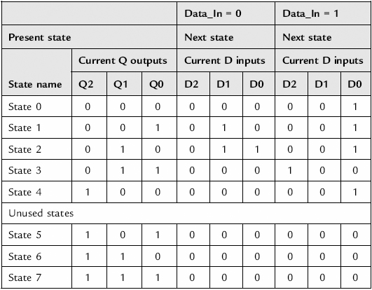
The state transition table (also referred to as a present state/next state table) for the 1001 sequence detector state diagram is shown in Table 11.1. Each possible input condition has its own column, and each row contains the present state and the next state for each possible input condition. The Detected output is defined in the truth table shown in Table 11.2.
Table 11.1 State transition table for the 1001 sequence detector

Table 11.2 Detected output for the 1001 sequence detector
| State | Detected |
| State 0 | 0 |
| State 1 | 0 |
| State 2 | 0 |
| State 3 | 0 |
| State 4 | 1 |
Using the circuit architecture shown in Figure 11.2, the input and output combinational logic blocks are created. Each state is created using the outputs from the sequential logic circuit element block. Flip-flops form a register whose outputs produce a binary value that defines one of the states. It is common to create the states as a straight binary count. Using n-flip-flops, 2n states are possible in the register output. However, any count sequence could be used. For example, one-hot encoding uses n-flip-flops to represent n states. In the one-hot encoding scheme, to change from one state to the next, only two flip-flop outputs will change (the first from a 1 to a 0, and the second from a 0 to a 1). The advantage of this scheme is less combinational logic to create the next state values.
11.2 Level-Sensitive Latches and Edge-Triggered Flip-Flops
The two sequential logic circuit elements are the latch and the flip-flop. These elements store a logic value (0 or 1). The basic latches and flip-flops are:
11.3 The D-Latch and D-Type Flip-Flop
The basic D-latch circuit symbol, shown in Figure 11.5, includes two inputs, the data input (D, value to store) and the control input (C). There is one output (Q).

Figure 11.5 D-latch
In the D-latch, when the C input is at a logic 1, the Q output is assigned the value of the D input. When the C input is a logic 0, the Q output holds its current value even when the D input changes. In addition, many D-latches also include a logical inversion of the Q output (the NOT-Q output) as an additional output.
Latches are normally designed as part of normal circuit operation. However, a problem can occur when writing HDL code in that a badly written design will create unintentional latches. When a design description is synthesized, the synthesis tool will infer latches. In VHDL, two common coding mistakes that result in inferred latches are:
• an If statement without an Else clause;
• a register description without a clock rising or falling edge construct.
An example of an If statement without an Else clause in VHDL is shown in Figure 11.6. Here, a circuit has two input signals (Data_In and Enable) and one output signal (Data_Out). The output is the logical value of the Data_In input when the Enable input is a logic 1. The operation of the circuit is defined on lines 20 to 30 of the code.

Figure 11.6 If statement without an Else clause
The RTL schematic for this design, as synthesized and viewed as a schematic within the Xilinx® ISE™ tools, is shown in Figure 11.7. The latch is the LD symbol in the middle of the schematic view.

Figure 11.7 Schematic of inferred latch design
This unintentional latch can be removed by including the Else clause, as shown in Figure 11.8. Here, when the Enable input is a 0, then the Data_Out output is a logic 0 also. The schematic for this design, as synthesized and viewed as a RTL schematic within the Xilinx® ISE™ tools, is shown in Figure 11.9. This forms a circuit with a single two-input AND gate. The operation of the circuit is defined on lines 20 to 34 of the code.

Figure 11.8 If statement with an Else clause
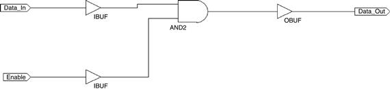
Figure 11.9 Schematic of the design with an Else clause
The basic D-type flip-flop circuit symbol is shown in Figure 11.10, with two inputs— the data input (D, value to store) and the clock input (CLK)—and one output (Q).
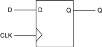
Figure 11.10 D-type flip-flop
In the D-type flip-flop, when the CLK input changes from a 0 to a 1 (positive edge triggered) or from a 1 to a 0 (negative edge triggered), the Q output is assigned the value of the D input. When the CLK input is steady at a logic 0 or a 1, the Q output holds its current value even when the D input changes.
It is common, however, for the flip-flop to have a reset or set input to initialize the output Q to either logic 0 (reset) or logic 1 (set). This reset/set input can either be asynchronous (independent of the clock input) or synchronous (occurs in a clock edge) and active high (reset/set occurs when the signal is a logic 1) or active low (reset/set occurs when the signal is a logic 0). The circuit symbol for the D-type flip-flop with active low reset is shown in Figure 11.11.
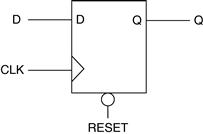
Figure 11.11 D-type flip-flop with active low reset
The circle on the reset input indicates an active low reset: if no circle is used, then the flip-flop is active high reset. Many D-type flip-flops also include a logical inversion of the Q output (the NOT-Q output) as an additional output. The circuit symbol for the D-type flip-flop with a NOT-Q output is shown in Figure 11.12.

Figure 11.12 D-type flip-flop with active low reset and not-Q output
When a D-input change is to be stored in the flip-flop, specific timing requirements must be considered for the inputs of the flip-flop in both set-up (how long before the clock input must the D input be static?) and hold (how long after the clock input must the D input be static?). This is shown in Figure 11.13. If these times are violated, then problems with the flip-flop operation will occur.

Figure 11.13 D-type flip-flop set-up and hold times
A potential problem known as metastability can occur when flip-flop set-up and hold times are violated. The flip-flop enters a metastable state in which the output is unpredictable until, after some time, the output becomes a logic 0 or 1. In the metastable state, the flip-flop output oscillates between 0 and 1. A simple way to design a circuit that avoids this problem is to ensure that the clock period is long enough to allow the metastable state to resolve itself and to account for signal delays (resulting from logic gates and interconnect) in the path of the next flip-flop in the circuit.
11.4 Counter Design
The counter is a sequential logic circuit that acts autonomously to perform the functions of a number counter changing its count state (value) on a clock edge. In the following discussions, then:
• positive edge triggered, asynchronous active low or high D-type flip-flops will be used;
In addition, the output from the counter either can be taken directly from the Q outputs of each flip-flop, or can be decoded using output combinational logic to form specific outputs for specific states of the counter.
Because the counter uses flip-flops, for n-flip-flops, there will be 2n possible combinations of output for the flip-flops. A counter might use all possible states or might use only a subset of the possible states. When a subset is used, the counter should be designed so that it will not enter unused states during normal operation. In addition, it is good practice to design the circuit so that if it does enter one of the unused states, it will have a known operation. For example, if an unused state is entered, the next state would always be the reset state for the counter.
Example 11.1 Three-Bit Straight Binary Up-Counter
Consider a three-bit straight binary up-counter as shown in Figure 11.14, using two inputs, clock and reset, and three outputs. The counter outputs are taken directly from the Q outputs of each flip-flop (Q2, Q1, and Q0), where Q2 is the MSB and Q0 is the LSB.

Figure 11.14 Three-bit straight binary up-counter
The design process begins by creating the state transition diagram (Figure 11.15) and the state transition table. The counter is designed to reset (i.e., when reset is a logic 0) to a count of 0002 (010), which will be state 0. When the reset is removed (i.e., when reset becomes a logic 1), then the counter will count through the sequence 0, 1, 2, 3, 4, 5, 6, 7, 0, etc. This means that when the counter output reaches 1112 (state 7), it will automatically wrap around back to 0002.
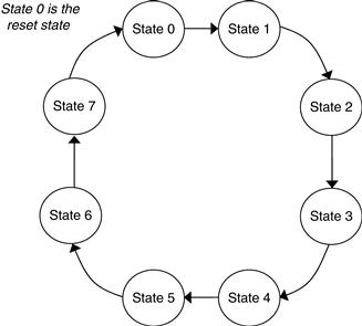
Figure 11.15 Three-bit straight binary up-counter state transition diagram
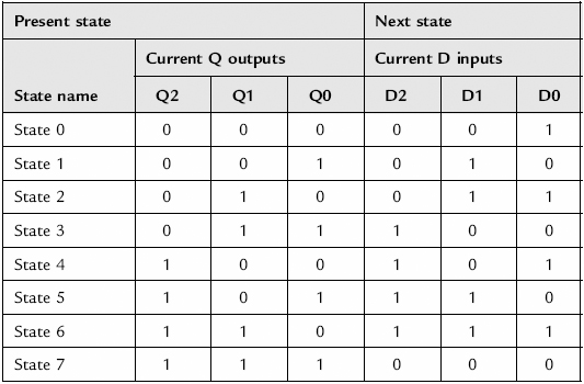
Each state in the counter will be encoded by the Q outputs of the D-type flip-flops, as shown in Table 11.3, so that it produces the required straight binary count sequence.
Table 11.3 Three-bit straight binary up-counter state encoding

The state transition table for the counter can then be created (Table 11.4). For the next state logic, the Q output for each flip-flop in the next state is actually the D input for each flip-flop in the current state. In this view of the state transition table, the current Q outputs and the current D inputs (next state Q outputs) are defined.
Table 11.4 Three-bit straight binary up-counter state transition table
The Boolean logic expression can be created for each of the D inputs so that the counter of the form shown in Figure 11.16 is created. Here, the next state logic for each flip-flop (Dffn) uses a combination of the Q and NOT-Q outputs from each flip-flop. Manipulation of the Boolean logic expression, the use of truth tables, and Karnaugh maps allow the designer to create a Boolean logic expression of a required form.

Figure 11.16 Three-bit counter structure
An example of the logic for each flip-flop D input developed using the Karnaugh map is shown in Figure 11.17. Figure 11.18 shows the schematic developed for the counter in which each D-type flip-flop only has a Q output, and the NOT-Q output is created using a discrete inverter. Additionally, each D-type flip-flop has an asynchronous active high reset that must be initially inverted so that the design reset input sees an asynchronous active low reset circuit.

Figure 11.17 Three-bit up-counter D-input Boolean expressions
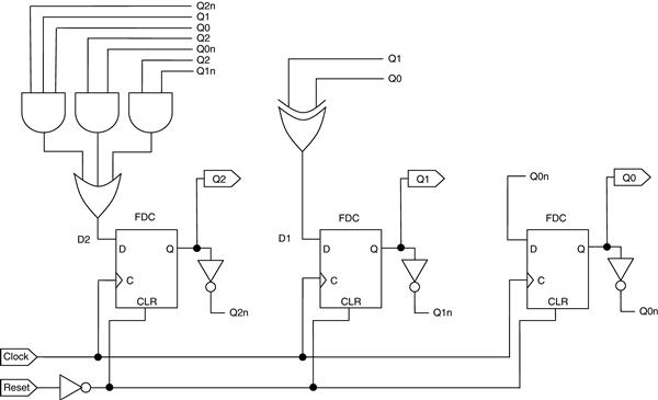
Figure 11.18 Circuit schematic for three-bit up-counter
Example 11.2 Three-Bit Straight Binary Down-Counter
Consider a three-bit straight binary down-counter, as shown in Figure 11.19 with two inputs, clock and reset. The counter outputs are taken directly from the Q outputs of each flip-flop (Q2, Q1, and Q0), where Q2 is the MSB and Q0 is the LSB. This is similar to the up-counter, except now the binary count is downward.

Figure 11.19 Three-bit straight binary down-counter
The design process begins by creating the state transition diagram (Figure 11.20) and the state transition table. The counter is designed to reset to a count of 0002 (010). When the reset is removed (i.e., becomes a logic 1), the counter will count through the sequence 0, 7, 6, 5, 4, 3, 2, 1, 0, etc. This means that when the counter output reaches 0002, it will automatically wrap around back to 1112.

Figure 11.20 Three-bit straight binary down-counter state transition diagram
Each state in the counter is encoded by the Q outputs of the D-type flip-flops, as shown in Table 11.5.
Table 11.5 Three-bit straight binary down-counter state encoding

The state transition table for the counter can then be created (Table 11.6). For the next state logic, the Q output for each flip-flop is actually the D input for each flip-flop in the current state. In this view of the state transition table, the current Q outputs and the current D inputs (next state Q outputs) are defined.
Table 11.6 Three-bit straight binary down-counter state transition table

The Boolean logic expression can be created for each of the D inputs so that the counter of the form shown in Figure 11.16 is created. The next state logic for each flip-flop uses a combination of the Q and NOT-Q outputs from each flip-flop.
Manipulation of the Boolean logic expression, use of truth tables, and Karnaugh maps allows the designer to create a Boolean logic expression of a required form.
An example of the logic for each flip-flop D input developed using the Karnaugh map is shown in Figure 11.21; Figure 11.22 shows a schematic for the counter. Each D-type flip-flop has only a Q output, and the NOT-Q output is created using a discrete inverter. Additionally, each D-type flip-flop has an asynchronous active high reset that must be initially inverted so that the design reset input sees an asynchronous active low reset circuit.

Figure 11.21 Three-bit down-counter D input Boolean expressions

Figure 11.22 Xilinx ISE™ schematic for three-bit down-counter
Example 11.3 Divide-by-5 Circuit
Consider a circuit that receives a clock signal and produces a single output pulse on every fifth clock input pulse. This simple divide-by-5 circuit, shown in Figure 11.23, can be used in a clock divider circuit.

Figure 11.23 Divide-by-5 circuit I/O
To create this output signal (Divided_Clock), a counter with five count states (0, 1, 2, 3, 4) is created and the output decoded using combinational logic so that on state 4 of the count, the output is a logic 1 only. This ensures that when the counter is reset (either at power on or by an external circuit), the output will be a logic 0. This arrangement is shown in Figure 11.24.

Figure 11.24 Divide-by-5 circuit
The design process begins by creating the state transition diagram (Figure 11.25) and the state transition table. The counter is designed to reset (into state 0) to a count value of 0002 (010). When the reset is removed (i.e., becomes a logic 1), then the counter will count through the sequence 0, 1, 2, 3, 4, 0, etc. When the counter output reaches 1002, it will automatically wrap around back to 0002.

Figure 11.25 Divide-by-5 circuit state transition diagram
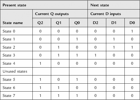
Each state in the counter is encoded by the Q outputs of the D-type flip-flops, as shown in Table 11.7.
Table 11.7 Divide-by-5 circuit state encoding

The state transition table for the counter can then be created (Table 11.8). For the next state logic, the Q output for each flip-flop in the next state is actually the D input for each flip-flop in the current state. In this view of the state transition table, the current Q outputs and the current D inputs (next state Q outputs) are defined. The unused states are also shown and are set so that if they are entered, the next state will be state 0.
Table 11.8 Divide-by-5 circuit state transition table
A Boolean logic expression can be created for each of the D inputs so that a counter of the form shown in Figure 11.16 is created. Here, the next state logic for each flip-flop uses a combination of the Q and NOT-Q outputs from each flip-flop. Manipulation of the Boolean logic expression, the use of truth tables, and Karnaugh maps allow the designer to create a Boolean logic expression of a required form.
An example of the logic for each flip-flop D input developed using the Karnaugh map is shown in Figure 11.26. Figure 11.27 shows the schematic developed for the counter, in which each D-type flip-flop only has a Q output, and the NOT-Q output is created using a discrete inverter. Additionally, each D-type flip-flop has an asynchronous active high reset that must be initially inverted so that the design reset input sees an asynchronous active low reset circuit.

Figure 11.26 Divide-by-5 D input Boolean expressions
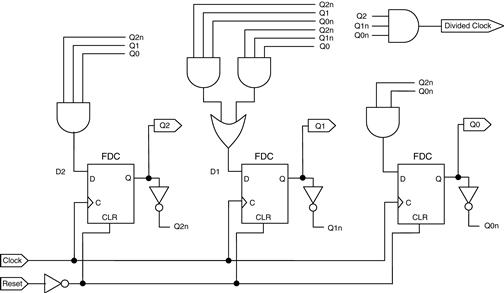
Figure 11.27 Xilinx ISE™ schematic for the divide-by-5 circuit
The output combinational logic is provided in the truth table shown in Table 11.9. The output is a logic 1 only when the counter is in state 4.
Table 11.9 Three divide-by-5 circuit output logic decodings

The Boolean logic expression for the Divided_Clock output is given as:
![]()
11.5 State Machine Design
The sequential logic circuit is designed either to react to an input, called a state machine in this text, or to be autonomous, in which no inputs control circuit operation. Figure 11.28 shows the basic structure of the state machine.
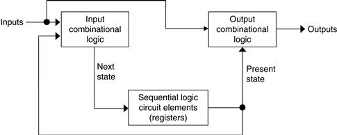
Figure 11.28 State machine structure
In the following discussions:
• positive edge triggered, asynchronous active low or high D-type flip-flops will be used;
In addition, the output from the state machine either can be taken directly from the Q outputs of each flip-flop or can be decoded using output combinational logic to form specific outputs for specific states of the counter.
The state machine uses flip-flops, so for n-flip-flops, there are 2n possible combinations of output. A state machine might use all possible states or might use only a subset of the possible states. When a sub-set is used, the state machine should be designed so that in normal operation, it will not enter the unused states. However, it is good practice to design the circuit so that if it did enter one of the unused states, it will have a known operation. For example, if an unused state is entered, the next state would always be the reset state for the state machine.
The state machine will be based on either a Moore machine or Mealy machine. In the Moore machine, the outputs will be a function of the present state only. As such, the outputs will be valid while the state machine is within this state and will not be valid during state transitions. In the Mealy machine, the output is a function of the present state and current inputs. As such, the output of the Mealy machine will change immediately whenever there is a change on the input while the output of the Moore machine would be synchronized to the clock.
Example 11.4 Traffic Light Sequencer
Consider a state machine design to control a set of traffic lights that moves from green to amber to red and back to green whenever a person pushes a button. This is shown in Figure 11.29. There are three inputs—clock, reset, and change—and three outputs—red, amber, and green.
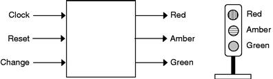
Figure 11.29 Three-bit straight binary up-counter
The light begins on green (when the circuit is reset) and stays in the green state when change is a logic 0. When change becomes a 1 (for a duration of 1 clock cycle), the lights will change according to the following sequence:
![]()
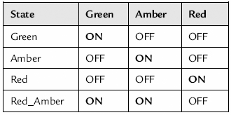
The four states and their corresponding outputs (ON = logic 1, OFF = logic 0) are defined in Table 11.10.
Table 11.10 Traffic light sequence
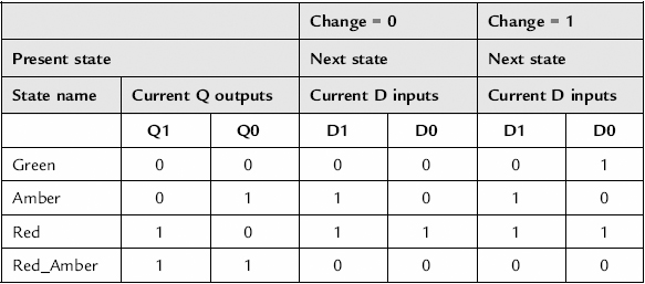
The state machine is designed so that when a change input is detected, the lights will change from green to red and back to green. It will then wait for another change input to be detected. During the light changes, the value of change is considered a Don’t care condition (i.e., it could be a logic 0 or 1).
The design process begins by creating the state transition diagram (Figure 11.30) and the state transition table. There are four distinct states, so two D-type flip-flops are used (where n = 2, giving 2n = 4 possible states). The state machine is designed to reset (i.e., when reset is a logic 0) to a count of 002 (010), which is the green state. When the reset is removed (i.e., when reset becomes a logic 1), the state will count through the sequence Green, Amber, Red, Red_Amber, Green, etc. when the Change button is pushed, and when the state machine output reaches 112 (state Red_Amber), it will automatically wrap around back to Green. State machine changes are summarized below: ate will count through the sequence Green, Amber, Red, Red_Amber, Green, etc, when the Change button is pushed, and when the state machine output reaches 112 (state Red_Amber), it will automatically wrap around back to Green. State machine changes are summarized below:
• State is green and input (change) is a logic 0: state remains green.
• State is green and input (change) is a logic 1: state changes to amber.
• State is amber and input (change) is a logic 0 or 1: state changes to red.
• State is red and input (change) is a logic 0 or 1: state changes to red_amber.
• State is red_amber and input (change) is a logic 0 or 1: state changes to green.

Figure 11.30 Traffic light controller circuit state transition diagram (Moore machine)
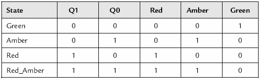
Each state in the state machine will be encoded by the Q outputs of the D-type flip-flops, as shown in Table 11.11.
Table 11.11 Divide-by-5 circuit state encoding
| State | Q1 | Q0 |
| Green | 0 | 0 |
| Amber | 0 | 1 |
| Red | 1 | 0 |
| Red_Amber | 1 | 1 |
The state transition table for the counter can then be created, as shown in Table 11.12. For the next state logic, the Q output for each flip-flop in the next state is actually the D input for each flip-flop in the current state. In this view of the state transition table, the current Q outputs and the current D inputs (next state Q outputs) are defined. The change input is included in the state transition table, and the state machine moves into one of two possible next states.
Table 11.12 Traffic light controller state transit
The Boolean logic expression can be created for each D input so that a state machine like that shown in Figure 11.28 is created. The next state logic for each flip-flop uses a combination of the Q and NOT-Q outputs from each flip-flop along with the change input. Manipulation of the Boolean logic expression, the use of truth tables, and Karnaugh maps allow the designer to create the required Boolean logic expression.
The logic for each flip-flop D input can be developed using the truth table. As there is only one D input to each flip-flop, but two possible input conditions (depending on the value of change), Boolean logic expressions for each possible input are created and the results ORed together to determine the D input of each flip-flop. This idea is shown in Figure 11.31. The resulting Boolean logic expression should then be minimized.

Figure 11.31 ORing the logic expressions to form the flip-flop D input
An example for the Boolean logic expressions for each of the flip-flops is as follows:
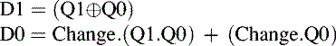
This shows that the D1 input is actually independent of the change input logic value. The output combinational logic is provided in the truth table shown in Table 11.13.
Table 11.13 Traffic light controller output logic decoding
The Boolean logic expressions for the outputs are given as:

Figure 11.32 shows a schematic developed for the counter in which each D-type flip-flop has only a Q output and the NOT-Q output is created using a discrete inverter. Additionally, each D-type flip-flop has an asynchronous active high reset that must be initially inverted so that the design reset input sees an asynchronous active low reset circuit.

Figure 11.32 Circuit schematic for the traffic light controller
Example 11.5 1001 Sequence Detector
Consider the circuit that is to detect the sequence 1001 on a serial bit-stream data input and produce a logic 1 output when the sequence has been detected, as shown in Figure 11.33. The state machine will have three inputs—one Data_In to be monitored for the sequence and two control inputs, Clock and Reset—and one output, Detected. Such a state machine could be used in a digital combinational lock circuit.
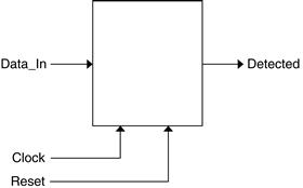
Figure 11.33 1001 sequence detector
The design process begins by creating the state transition diagram (Figure 11.34) and the state transition table. There are five distinct states, so three D-type flip-flops are used (where n = 3, giving 2n = 8 possible states, although only five states are used). The state machine is designed to reset (i.e., when Reset is a logic 0) to a count of 0002 (010), which will be the state 0 state. When the reset is removed (i.e., when reset becomes a logic 1), then the state machine becomes active. State machine changes are summarized below:
• At state 0 and input (Data_In) is a logic 0: state remains in state 0.
• At state 0 and input (Data_In) is a logic 1: state changes to state 1.
• At state 1 and input (Data_In) is a logic 0: state changes to state 2.
• At state 1 and input (Data_In) is a logic 1: state remains in state 1.
• At state 2 and input (Data_In) is a logic 0: state changes to state 3.
• At state 2 and input (Data_In) is a logic 1: state changes back to state 1.
• At state 3 and input (Data_In) is a logic 0: state changes back to state 0.
• At state 3 and input (Data_In) is a logic 1: state changes to state 4.
• At state 4 and input (Data_In) is a logic 0: state changes back to state 0.
• At state 4 and input (Data_In) is a logic 1: state changes back to state 1.
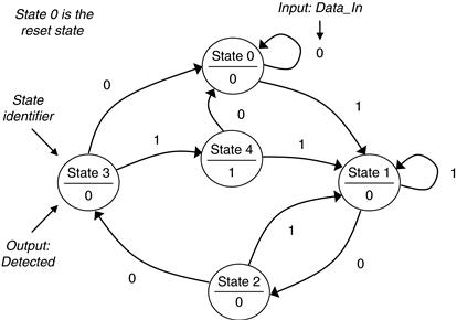
Figure 11.34 1001 sequence detector state transition diagram (Moore machine)
Whenever an unused state is encountered, the state machine is designed to enter state 0 on the next clock rising edge.
Each state in the counter is encoded by the Q outputs of the D-type flip-flops, as shown in Table 11.14.
Table 11.14 1001 sequence detector state encoding

The state transition table for the counter can then be created, as shown in Table 11.15. For the next state logic, the Q output for each flip-flop in the next state is actually the D input for each flip-flop in the current state. In this view of the state transition table, the current Q outputs and the current D inputs (next state Q outputs) are defined. The change input is included in the state transition table, and the state machine can move into one of two possible next states.
Table 11.15 1001 sequence detector state transition table
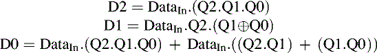
An example for the Boolean logic expressions for each of the flip-flops is as follows:
The output combinational logic is provided in the truth table shown in Table 11.16.
Table 11.16 1001 sequence detector output logic decoding

The Boolean logic expressions for the output is given as:
![]()
Figure 11.35 shows a schematic developed for the counter in which each D-type flip-flop has only a Q output and the NOT-Q output is created using a discrete inverter. Additionally, each D-type flip-flop has an asynchronous active high reset that must be initially inverted so that the design reset input sees an asynchronous active low reset circuit.

Figure 11.35 Circuit schematic for the 1001 sequence detector
11.6 Moore Versus Mealy State Machines
Sequential logic circuit designs create counters and state machines. The state machines are based on either the Moore machine or the Mealy machine, shown in Figure 11.36.

Figure 11.36 Moore and Mealy state machines
The diagrams shown in Figure 11.36 are a modification of the basic structure identified in Figure 11.1 by separating the combinational logic block into two blocks, one to create the next state logic (inputs to the state register that store the state of the circuit) and the output logic:
• In the Moore machine, the outputs are a function only of the present state only.
• In the Mealy machine, the outputs are a function of the present state and the current inputs.
The types of circuits considered here will be synchronous circuits in that activity occurs under the control of a clock control input, these are synchronous circuits. A number of possible circuits can be formed to produce the required circuit functionality.
11.7 Shift Registers
The D-type flip-flops can be connected so that the Q output of one flip-flop is connected to the D input of the next flip-flop, as shown in Figure 11.37. With a single input (Data_In), a serial bit-stream can be applied to the circuit. Whenever a clock edge occurs, the D input of a flip-flop is stored and presented as the Q output of that flip-flop.

Figure 11.37 Four-bit shift register (serial in, serial out)
If there are n-flip-flops in the circuit, the serial bitstream applied at the input appears at the output (as Data_Out) after n clock cycles. The serial bitstream input is available as a serial bitstream output, which is referred to as a serial-in, serial-out shift register because the input is shifted by the clock signal to become the output.
Modifications to this circuit allow parallel input to the shift register (a parallel data load, rather than a serial data load) and parallel output. A shift register that provides for serial input along with serial and parallel output is shown in Figure 11.38.

Figure 11.38 Four-bit shift register (serial in, parallel and serial out)
11.8 Digital Scan Path
The shift register is used to support circuit and system testing. This arrangement forms a scan path [Ref. 11.1]. Scan path testing is the main method to provide access for internal node controllability and observability of digital sequential logic circuits, where:
• controllability is the ability to control specific parts of a design to set particular logic values at specific points.
• observability is the ability to observe the response of a circuit to a particular circuit stimulus.
In scan path, the circuit is designed for two modes of operation:
• normal operating mode, in which the circuit is running according to its required end-user function; and
• scan test mode, in which logic values are serially clocked into circuit flip-flop elements from an external signal source, and the results are serially clocked out for external monitoring.
The incorporation of a scan path into a design requires additional inputs and outputs specifically used for the test procedure. These inputs and outputs, and the scan test circuitry, are not used by the end user.
Scan Test Output:
• Scan data out (SDO) scans the data (results) that are serially clocked out of the scan path for external monitoring.
Using the basic circuit arrangement shown in Figure 11.38, the D-type flip-flops within the sequential logic circuit are put into a serial-in, serial-out shift register as shown in Figure 11.39, showing SDI and SDO. The parallel outputs (Q0, Q1, Q2, and Q3) form inputs to the combinational logic within the design.
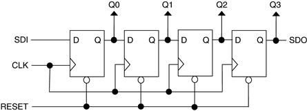
Figure 11.39 Scan test shift register
A typical scan path test arrangement is shown in Figure 11.40, including the combinational logic block and D-type flip-flops. Each flip-flop has a common clock and reset input. Between the flip-flop D input and the combinational logic (the next state logic), a two-input multiplexer is inserted. The first data input to the multiplexer is the output from the next state logic. The second data input comes from the Q output of a flip-flop. This allows either of these signals to be applied to the D input of the flip-flop using the select input on the multiplexer (connected to SE).

Figure 11.40 Scan path insertion using D-type flip-flops and multiplexers
In normal operating mode, the next state logic is connected to the flip-flop D input. In scan test mode, the Q output from a previous flip-flop is connected to the flip-flop D input. This isolates the flip-flop from the next state logic, and the flip-flops form a shift register of the form shown in Figure 11.39. Test data can therefore be scanned in (using the SDI input), and test results can be scanned out (using the SDO output). An example operation of this scan path follows:
1. The circuit is put into scan test mode (by control of the SE). The test data is serially scanned into the design to set the flip-flop Q outputs to known values (i.e., to put the circuit into a known, initial state) by applying the test data to the SDI pin.
2. The circuit is put back into its normal operating mode and operated for a set number of clock cycles.
3. The circuit is again put into scan test mode. The results of the test are stored on the Q outputs of the flip-flops and serially scanned out and monitored on the SDO pin.
4. The monitored values are compared with the expected values, and the circuit is then checked to see if it has passed (expected values received) or failed (the circuit output is not as expected) the test.
The arrangement shown in Figure 11.40 uses a discrete multiplexer and D-type flip-flop to create the scan path. In many circuits, these functions are combined into a single scan D-type flip-flop circuit element, as shown in Figure 11.41. This has the same logic functionality as a discrete flip-flop and multiplexer arrangement, but is optimized for size and speed of operation. It has two data inputs (D, normal data, and SD, scan data input) and a scan enable (SE) control input to select between normal and scan test modes, in addition to the clock, reset (and/or set) inputs and Q/NOT-Q outputs.
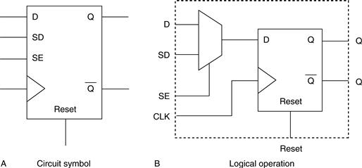
Figure 11.41 Scan D-type flip-flop
REFERENCES
[11.1] Grout IA. Integrated Circuit Test Engineering Modern Techniques Springer 2006; ISBN 1-84628-023-0.