
Chapter 4
Bipolar Transistors
Unlike semiconductor diodes, transistors did not see active service in the Second World War; they were born several years too late. In 1948 it was discovered that if a point contact diode detector were equipped with two cat’s whiskers rather than the usual one, spaced very close together, the current through one of them could be influenced by a current through the other. The crystal used was germanium, one of the rare earths, and the device had to be prepared by discharging a capacitor through each of the cat’s whiskers in turn to “form” a junction. Over the following years, the theory of conduction via junctions was elaborated as the physical processes were unraveled, and the more reproducible junction transistor replaced point contact transistors.
However, the point contact transistor survives to this day in the form of the standard graphical symbol denoting a bipolar junction transistor (Figure 4.1(A)). This has three separate regions, as in Figure 4.1(B), which shows (purely diagrammatically and not to scale) an NPN junction transistor. With the base (another term dating from point contact days) short-circuited to the emitter, no collector current can flow since the collector/base junction is a reverse biased diode, complete with depletion layer as shown. The higher the reverse bias voltage, the wider the depletion layer, which is found mainly on the collector side of the junction since the collector is more lightly doped than the base. In fact, the pentavalent atoms which make the collector n-type are found also in the base region. The base is a layer which has been converted to p-type by substituting so many trivalent (hole donating) atoms into the silicon lattice, e.g., by diffusion or ion bombardment, as to swamp the effect of the pentavalent atoms. So holes are the majority carriers in the base region, just as electrons are the majority carriers in the collector and emitter regions. The collector “junction” turns out then to be largely notional; it is simply that plane for which on one side (the base) holes or p-type donor atoms predominate, while on the other (the collector) electrons or n-type donor atoms predominate, albeit at a much lower concentration.

Figure 4.1 The bipolar transistor. (A) Bipolar transistor symbols. (B) NPN junction transistor, cut-off condition. Only majority carriers are shown. The emitter depletion region is very much narrower than the collector depletion region because of reverse bias and higher doping levels. Only a very small collector leakage current Icb flows. (C) NPN small signal silicon junction transistor, conducting. Only minority carriers are shown. The DC common emitter current gain is hFE = IcIb, roughly constant and typically around 100. The AC small signal current gain is hfe = dIc/dIb = ic/ib. (D) Collection current versus collector/emitter voltage, for an NPN small signal transistor (BC 107/8/9). (E) Collector current versus collector/emitter voltage, for an NPN power transistor. (F) hFE versus collector current for an NPN small signal transistor. (G) Collector current versus base/emitter voltage for an NPN small signal transistor.
(Parts (D) to (G) reproduced by courtesy of Philips Components Ltd.)
Figure 4.1(C) shows what happens when the base/emitter junction is forward biased. Electrons flow from the emitter into the base region and, simultaneously, holes flow from the base into the emitter. The latter play no useful part in transistor action: they contribute to the base current but not to the collector current. Their effect is minimized by making the n-type emitter doping a hundred times or more heavier than the base doping, so that the vast majority of current flow across the emitter/base junction consists of electrons flowing into the base from the emitter. Some of these electrons flow out of the base, forming the greater part of the base current. But most of them, being minority carriers (electrons in what should be a p-type region) are swept across the collector junction by the electric field gradient existing across the depletion layer. This is illustrated (in diagrammatic form) in Figure 4.1(C), while Figure 4.1(D) shows the collector characteristics of a small-signal NPN transistor and Figure 4.1(E) those of an NPN power transistor. It can be seen that, except at very low values, the collector voltage has comparatively little effect upon the collector current, for a given constant base current. For this reason, the bipolar junction transistor is often described as having a “pentode-like” output characteristic, by an analogy dating from the days of valves. This is a fair analogy as far as the collector characteristic is concerned, but there the similarity ends. The pentode’s anode current is controlled by the g1 (control grid) voltage, but there is, at least for negative values of control grid voltage, negligible grid current. By contrast, the base/emitter input circuit of a transistor looks very much like a diode, and the collector current is more linearly related to the base current than to the base/emitter voltage (Figure 4.1(F) and (G)). For a silicon NPN transistor, little current flows in either the base or collector circuit until the base/emitter voltage Vbe reaches about +0.6V, the corresponding figure for a germanium NPN transistor being about +0.3V. For both types, the Vbe corresponding to a given collector current falls by about 2 mV for each degree centigrade of temperature rise, whether this is due to the ambient temperature increasing or due to the collector dissipation warming the transistor up. The reduction in Vbe may well cause an increase in collector current and dissipation, heating the transistor further and resulting in a further fall in Vbe. It thus behooves the circuit designer, especially when dealing with power transistors, to ensure that this process cannot lead to thermal runaway and destruction of the transistor.
Although the base/emitter junction behaves like a diode, exhibiting an incremental resistance of 25/Ie at the emitter, most of the emitter current appears in the collector circuit, as has been described above.
The ratio Ic/Ib is denoted by the svmbol hFE and is colloquially called the DC current gain or static forward current transfer ratio. Thus, if a base current of 10 μA results in a collector current of 3 mA—typically the case for a high-gain general purpose audio-frequency NPN transistor such as a BC109—then hFE = 300. As Figure 4.1(F) shows, the value found for hFE will vary somewhat according to the conditions (collector current and voltage) at which it is measured. When designing a transistor amplifier stage, it is necessary to ensure that any transistor of the type to be used, regardless of its current gain, its Vbe, etc., will work reliably over a wide range of temperatures: the no-signal DC conditions must be stable and well defined. The DC current gain hFE is the appropriate gain parameter to use for this purpose. When working out the stage gain or AC small-signal amplification provided by the stage, hfe is the appropriate parameter, this is the AC current gain dIc = dIb. Usefully, for many modern small-signal transistors there is little difference in the value of hFE and hfe over a considerable range of current, as can be seen from Figures 4.1(F) and 4.2(A) (allowing for the linear hFE axis in one and the logarithmic hfe axis in the other).
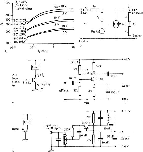
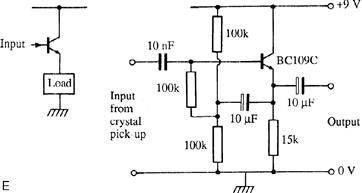
Figure 4.2 Small-signal amplifiers. (A) hfe versus collector current for an NPN small-signal transistor of same type as in Figure 4.4(F) (reproduced by courtesy of Philips Components Ltd.). (B) Common emitter equivalent circuit. (C) Common emitter audio amplifier. Ib = base bias or standing current; Ic = collector standing current; ic = useful signal current in load. (D) Common base RF amplifier. (E) Common collector high-input-impedance audio amplifier.
Once the AC performance of a transistor is considered, it is essential to allow for the effects of reactance. Just as there is capacitance between the various electrodes of a valve, so too there are unavoidable capacitances associated with the three electrodes of a transistor. The collector/base capacitance, though usually not the largest of these, is particularly important as it provides a path for AC signals from the collector circuit back to the base circuit. In this respect, the transistor is more like a triode than a pentode, and as such the Miller effect will reduce the high-frequency gain of a transistor amplifier stage, and may even cause an RF stage to oscillate due to feedback of in-phase energy from the collector to the base circuit.
One sees many different theoretical models for the bipolar transistor, and almost as many different sets of parameters to describe it: z, g, y, hybrid, s, etc. Some equivalent circuits are thought to be particularly appropriate to a particular configuration, e.g., grounded base, while others try to model the transistor in a way that is independent of how it is connected. Over the years numerous workers have elaborated such models, each proclaiming the advantages of his particular equivalent circuit.
Just one particular set of parameters will be mentioned here, because they have been widely used and because they have given rise to the symbol commonly used to denote a transistor’s current gain. These are the hybrid parameters which are generally applicable to any two-port network, i.e., one with an input circuit and a separate output circuit. Figure 4.3(A) shows such a two-port, with all the detail of its internal circuitry hidden inside a box—the well-known “black box” of electronics. The voltages and currents at the two ports are as defined in Figure 4.1(A), and I have used v and i rather than V and I to indicate small-signal alternating currents, not the standing DC bias conditions. Now v1, i1, v2, and i2 are all variables and their interrelation can be described in terms of four h parameters as follows:
![]() (4.1)
(4.1)

Figure 4.3 h parameters. (A) Generalized two-port black box. v and i are small-signal alternating qualities. At both ports, the current is shown as in phase with the voltage (at least at low frequencies), i.e., both ports are considered as resistances (impedances). (B) Transistor model using hybrid parameters. (C) h parameters of a typical small-signal transistor family.
(Reproduced by courtesy of Philips Components Ltd.)
![]() (4.2)
(4.2)
Each of the h parameters is defined in terms of two of the four variables by applying either of the two conditions i1 = 0 or v2 = 0:
![]() (4.3)
(4.3)
 (4.4)
(4.4)
![]() (4.5)
(4.5)
 (4.6)
(4.6)
Thus h11 is the input impedance with the output port short-circuited as far as AC signals are concerned. At least at low frequencies, this impedance will be resistive and its units will be ohms. Next, h21 is the current transfer ratio, again with the output circuit short-circuited so that no output voltage variations result: being a pure ratio, h21 has no units. Like h11 it will be a complex quantity at high frequencies, i.e., the output current will not be exactly in phase with the input current. Third, h12 is the voltage feedback ratio, i.e., the voltage appearing at the input port as the result of the voltage variations at the output port (again this will be a complex number at high frequencies). Finally, h22 is the output admittance, measured—like h12—with the input port open-circuit to signals. These parameters are called hybrid because of the mixture of units: impedance, admittance and pure ratios.
In equation (4.1) the input voltage v1 is shown as being the result of the potential drop due to i1 flowing through the input impedance plus a term representing the influence of any output voltage variation v2 on the input circuit. When considering only small signals, to which the transistor responds in a linear manner, it is valid simply to add the two effects as shown. In fact the hybrid parameters are examples of partial differentials: these describe how a function of two variables reacts when first one variable is changed while the other is held constant, and then vice versa. Here, v1 is a function of both i1 and v2—so h11 = ∂v1/∂i1 with v2 held constant (short-circuited), and h12 = ∂v1/∂v2 with the other parameter i1 held constant at zero (open-circuit). Likewise, i2 is a function of both i1 and v2; the relevant parameters h21 and h22 are defined by equations (4.4) and (4.6), and i2 is as defined in equation (4.2). Of course the interrelation of v1, i1, v2 and i2 could be specified in other ways: the above scheme is simply the one used with h parameters.
The particular utility of h parameters for specifying transistors arises from the ease of determining h11 and h21 with the output circuit short-circuited to signal currents. Having defined h parameters, they can be shown connected as in Figure 4.3(B). Since a transistor has only three electrodes, the dashed line has been added to show that one of them must be common to both the input and the output ports. The common electrode may be the base or the collector, but particularly important is the case where the input and output circuits have a common emitter.
Armed with the model of Figure 4.3(B) and knowing the source and load impedance, you can now proceed to calculate the gain of a transistor stage—provided you know the relevant values of the four h parameters (see Figure 4.3(C)). For example, for a common emitter stage you will need hie (the input impedance h11 in the common emitter configuration), hfe (the common emitter forward current transfer ratio or current gain corresponding to h21), hre (the common emitter voltage feedback ratio corresponding to h12) and hoe (the common emitter output admittance corresponding to h22). You will generally find that the data sheet for the transistor you are using quotes maximum and minimum values for hfe at a given collector current and voltage, and may well also include a graph showing how the typical or normalized value of hfe varies with the standing collector current Ic. Sometimes, particularly with power transistors, only hFE is quoted: this is simply the ratio Ic/Ib, often called the DC current gain or static forward current transfer ratio. As mentioned earlier, for most transistors this can often be taken as a fair guide or approximation for hfe (for example, compare Figures 4.1(F) and 4.2(a)). From these it can be seen that over the range 0.1 to 10 mA collector current, the typical value of hFE is slightly greater than that of hFE, so the latter can be taken as a guide to hfe, with a little in hand for safety. Less commonly you may find hoe quoted on the data sheet, while hie and hre are often simply not quoted at all. Sometimes a mixture of parameters is quoted; for example, data for the silicon NPN transistor type 2N930 quote hFE at five different values of collector current, and low-frequency (1 kHz) values for hib, hrb, hfe and hob—all at 5V, 1 mA. The only data given to assist the designer in predicting the device’s performance at high frequency are fT and Cobo. The transition frequency fT is the notional frequency at which |hfe| has fallen to unity, projected at −6dB per octave from a measurement at some lower frequency. For example, fT (min.) for a 2N918 NPN transistor is 600 MHz measured at 100 MHz, i.e., its common emitter current gain hfe at 100 MHz is at least 6. Cobo is the common base output capacitance measured at Ic = 0, at the stated Vcb and test frequency (10V and 140 kHz in the case of the 2N918).
If you were designing a common base or common collector stage, then you would need the corresponding set of h parameters, namely hib, hfb, hrb and hob or hic, hfc, hrc and hoc respectively. These are seldom available—in fact, h parameters together with z, v, i and transmission parameters are probably used more often in the examination hall than in the laboratory. The notable exception are the scattering parameters s, which are widely used in radio-frequency and microwave circuit design. Not only are many UHF and microwave devices (bipolar transistors, silicon and gallium arsenide field-effect transistors) specified on the data sheet in s parameters, but s parameter test sets are commonplace in RF and microwave development laboratories. This means that if it is necessary to use a device at a different supply voltage and current from that at which the data sheet parameters are specified, they can be checked at those actual operating conditions.
The h parameters for a given transistor configuration, say grounded emitter, can be compared with the elements of an equivalent circuit designed to mimic the operation of the device. In Figure 4.2(B)re is the incremental slope resistance of the base/emitter diode; it was shown earlier that this is approximately equal to 25/Ie where Ie is the standing emitter current in milliamperes. Resistance rc is the collector slope or incremental resistance, which is high. (For a small-signal transistor in a common emitter circuit, say a BC109 at 2 mA collector current, 15K would be a typical value: see Figure 4.3(C)). The base input resistance rb is much higher than 25/Ie, since most of the emitter current flows into the collector circuit, a useful approximation being hfe × 25/Ie. The ideal voltage generator μbc represents the voltage feedback h12 (hre in this case), while the constant current generator αcb represents h21 or hfe, the ratio of collector current to base current. Comparing Figures 4.2(B) and 4.3(B), you can see that h11 = rb + re, h12 = μbc, h21 = αcb and h22 = 1/(re+rc).
Not the least confusing aspect of electronics is the range of different symbols used to represent this or that parameter, so it will be worth clearing up some of this right here. The small-signal common emitter current gain is, as has already been seen, sometimes called αcb, but more often hfe; the symbol β is also used. The symbol αce or just α is used to denote the common base forward current transfer ratio hfb: the term gain is perhaps less appropriate here, as ic is actually slightly less than ie, the difference being the base current ib. It follows from this that β = α/(1− α). The symbols α and β have largely fallen into disuse, probably because it is not immediately obvious whether they refer to small-signal or DC gain: with hfe and hFE—or hfb and hFB—you know at once exactly where you stand.
When h parameters for a given device are available, their utility is limited by two factors: first, usually typical values only are given (except in the case of hfe) and second, they are measured at a frequency in the audio range, such as 1 kHz. At higher frequencies the performance is limited by two factors: the inherent capacitances associated with the transistor structure, and the reduction of current gain at high frequencies.
In addition to their use as small-signal amplifiers, transistors are also used as switches. In this mode they are either reverse biased at the base, so that no collector current flows or conducting heavily so that the magnitude of the voltage drop across the collector load approaches that of the collector supply rail. The transistor is then said to be bottomed, its Vce being equal to or even less than Vbe. For this type of large-signal application, the small-signal parameters mentioned earlier are of little if any use. In fact, if (as is usually the case) one is interested in switching the transistor on or off as quickly as possible, it can more usefully be considered as a charge-controlled rather than a current-controlled device. Here again, although sophisticated theoretical models of switching performance exist, they often involve parameters (such as rbb′, the extrinsic or ohmic part of the base resistance) for which data sheets frequently fail to provide even a typical value. Thus one is usually forced to adopt a more pragmatic approach, based upon such data sheet values as are available, plus the manufacturer’s application notes if any, backed up by practical in-circuit measurements.
Returning for the moment to small-signal amplifiers, Figure 4.2(C), (D) and (E) shows the three possible configurations of a single-transistor amplifier and indicates the salient performance features of each. Since the majority of applications nowadays tend to use NPN devices, this type has been illustrated. Most early transistors were PNP types; these required a radical readjustment of the thought processes of electronic engineers brought up on valve circuits, since with PNP transistors the “supply rail” was negative with respect to ground. The confusion was greatest in switching (logic) circuits, where one was used to the anode of a cut-off valve rising to the (positive) HT rail, this being usually the logic 1 state. Almost overnight, engineers had to get used to collectors flying up to −6V when cut off, and vice versa. Then NPN devices became more and more readily available and eventually came to predominate. Thus the modern circuit engineer has the great advantage of being able to employ either NPN or PNP devices in a circuit, whichever proves most convenient—and not infrequently both types are used together. The modern valve circuit engineer, by contrast, still has to make do without a thermionic equivalent of the PNP transistor.
A constant grumble of the circuit designer was for many years that the current gain hFE of power transistors, especially at high currents, was too low. The transistor manufacturers’ answer to this complaint was the Darlington, which is now available in a wide variety of case styles and voltage (and current) ratings in both NPN and PNP versions. The circuit designer had already for years been using the emitter current of one transistor to supply the base current of another, as in Figure 4.4(A). The Darlington compound transistor, now simply called the Darlington, integrates both transistors, two resistors to assist in rapid turn-off in switching applications, and usually (as in the case of the ubiquitous TIP120 series from Texas Instruments) an antiparallel diode between collector and emitter. Despite the great convenience of a power transistor with a value of hFE in excess of 1000, the one fly in the ointment is the saturation or bottoming voltage. In a small-signal transistor (and even some power transistors) this may be as low as 200 mV, though usually one or two volts, but in a power Darlington it is often as much as 2 to 4V. The reason is apparent from Figure 4.4(B): the Vce sat of the compound transistor cannot be less than the Vce sat of the first transistor plus the Vbe of the second.

Figure 4.4 (A) Darlington connected discrete transistors. (B) Typical monolithic NPN Darlington power transistor.
(Reproduced by courtesy of Philips Components Ltd.)
Reference
1. EDN . Harold P, ed. Current-feedback op-amps ease high-speed circuit design. 1988.