
Chapter 34
Microcontroller Toolbox
This chapter contains some miscellaneous topics that pull together multiple concepts from preceding chapters.
34.1 Microcontroller Supply and Reference
In many cases, you can minimize the effects that supply voltage can have by referencing your analog inputs to the supply voltage. Figure 34.1A shows a thermistor connected to an analog input and using a pull-up to a precision reference voltage. At first glance, it might appear that this is a very accurate design because the precision reference gives a repeatable voltage versus temperature at the analog input. The problem with this design is that the microcontroller is measuring the temperature using the supply voltage as a reference, so the overall accuracy is only as good as the microcontroller supply voltage.

Figure 34.1 Microcontroller supply reference
Figure 34.1B shows the same circuit, but with the thermistor referenced to the microcontroller supply. This provides a more repeatable result. If the thermistor is 10K and R1 is 10K, for example, the analog input to the microcontroller will always sense half the supply voltage regardless of what the supply voltage actually is. This method will work only if the analog input can be made to follow the supply voltage. This essentially means that the output being measured by the microcontroller is referenced to the supply. Note that just powering the sensor or sensor circuit from the microcontroller supply may not be sufficient. If the sensor circuit has its own internal reference that controls the output value, it will produce the same output regardless of variations in the supply voltage.
An alternative compensation method, for cases in which the input is independent of the microcontroller supply voltage, is shown in Figure 34.1C In this figure, a second analog input is used to measure the value of a precision reference diode. Of course, the microcontroller must have at least two analog inputs to take advantage of this technique. In operation, the microcontroller would use the reference diode to determine the error caused by the supply voltage. For example, if the reference diode is 2.5V and the supply voltage is 5V, the reference diode will produce a value of 8016 (128 decimal) when the voltage is converted (assume the internal ADCs are 8 bits). If the supply is 4.8V, the reference diode will convert to a value of 8516 (133 decimal). The microcontroller can use this value to correct the values from the independent input. In this case, the values read from that input will be multiplied by 128/133, or 0.96, to get the correct reading. Note, though, that the overall accuracy is only as good as the combined accuracy of the reference diode and whatever reference the external input is using. Finally, to make use of this technique, the microcontroller must have sufficient throughput to make the required calculations and memory to hold the math algorithms; this may be a problem on some small microcontrollers.
34.2 Resistor Networks
Some applications need better repeatability than you can get with standard 1% resistors, but don’t need the level of precision (and cost) of going to 0.1% resistors. Sometimes you can gain an advantage by using resistor networks. Resistor networks are typically specified with the same resistance tolerances as discrete resistors: 0.1%, 1%, and 5%. However, the matching between resistors within the same network is often twice as good as the absolute resistance accuracy. If your circuit uses multiple resistors of the same value, you can often get better accuracy by using a resistor network rather than discrete parts. Note, though, that this works only for resistors in the same package; it doesn’t work across packages.
Figure 34.2 shows a simple voltage divider. This circuit might be used to bring an analog input that swings between 0 and 8V down to the 0 to 5V range used by a microcontroller analog input. In the figure, both resistors are 10K. Ideally, the output voltage would be half the input voltage. However, if the resistors are 1% discrete parts, the output voltage may not be exactly half the input.

Figure 34.2 Resistor voltage divider
Say that R1 is high by 1% and equals 10,100 ohms, and R2 is low by 1% and equals 9900 ohms. The output is given by the following equation:
![]()
which is incorrect by 1%, the tolerance of the resistors.
Now, say that R1 and R2 are resistors that are in the same resistor network package. The specified resistance is 1%, but the part-to-part variation is 0.5%. If R1 is high by 1%, it will be 10,100 ohms, as before. However, because parts within the network package can only vary by 0.5%, R2 cannot be less than 10,049.5. As a result, the output will be:
![]()
which is within 0.25%, of the ideal value.
34.3 Multiple Input Control
In some cases a system will have multiple inputs. For example, you might be controlling a telescope that is taking pictures of clouds. For some reason (perhaps to protect sensitive optics coatings), you don’t want to aim the telescope at the sun (Figure 34.3). In this case, one of the inputs would be the position of the sun, probably determined by the date and time of day. You would also have as inputs the telescope’s current position and the desired position.

Figure 34.3 Telescope pointing example
This is a good example of a two-input problem, because the position of the sun is not fixed. You can’t just use a table to look up the move path because the position of the sun varies. To move the telescope without crossing the path of the sun, you can take two approaches.
The first approach is to calculate the direct path, determine that it crosses the sun’s path, then calculate a new path that just misses the sun. This is illustrated in Figure 34.3A and 34.3B. This calculation may be complicated and time-consuming, especially on a microcontroller or other system with limited capability.
A simpler approach is to calculate the position of the sun and then calculate a path that remains as far as possible from the sun. One way to do this is to divide the telescope range into a grid of, say, 8 or 16 regions. When calculating the move path, any region overlapped by the sun is avoided. A typical example is shown in Figure 34.3C. Figure 34.3D shows how the move area can be subdivided into 16 regions.
Another alternative would be to find a sunless path to the perimeter of the motion circle, and then determine which way to move around the circle to avoid the sun. In the example shown, either direction would work, but if the sun were on the perimeter of the motion circle, the direction would have to be determined.
You could make the path decision table driven by having two move paths from any region to any other region. One path would be a straight line and the other path would avoid any region in common with the first path. In this way, you could determine a safe path by checking the straight line move for “interference” from the sun. If the straight line path goes through a region containing the sun, just pick the other path. Once in the target region, calculate a straight line move to the desired point. This method has the advantage of minimizing calculation requirements for simple processors.
The foregoing assumes that the system requirements don’t include taking photos of any region containing the sun. If you did have to take photos right next to the sun, you could make the regions smaller or you could have multiple paths from any region to any other, arriving at the destination from different directions.
Although the telescope example is very specific, the general principles are applicable to many similar multiple input problems, such as:
• multihead fluid pipetting systems in which the pipettes can interfere with each other;
• a heating system in which the maximum safe heater power depends on a fluid level;
• a stepper motor with resonance points that depend on the load;
• a valve control system in which valve closing/opening speed depends on fluid viscosity and flow rate—variable closing/opening time might be required to avoid “water hammer” or similar effects; and
• a heater or cooler system in which the intent is to quickly get the target to a specific temperature and where the amount of heating or cooling applied depends on the size and initial temperature of the target.
Another example of multiple input systems is the need to adjust system parameters based on an input—for example, from a heater. In this example, the proportional (or PID) control might have an offset which had to be adjusted for varying loads and ambient conditions. A large load or very cold ambient temperature might need a larger offset to maintain the temperature. In a case like this, additional sensors may be needed to measure these parameters. The system could calculate parameters such as the offset and/or gain, or a set of tables could be used to select the values based on the values of the additional input parameters.
34.4 AC Control
Some designs require control of AC power to turn on lights, motors, heaters, or other AC devices. The simplest method of controlling such devices is with solid-state relays (SSRs), as shown in Figure 34.4 An SSR consists of an optoisolator driving an SCR or triac. The internal optoisolator is selected by the manufacturer to ensure that it will be capable of driving the SCR or triac. Some SSRs have heatsink plates on the back that need to be bolted to a metal chassis or heatsink to avoid overheating the SSR.

Figure 34.4 SSR
In many cases you need to perform zero crossing switching. This consists of switching the load only when the AC signal crosses zero (Figure 34.5). If the AC signal is switched when the voltage is not zero, then the load will see a sudden jump in the applied voltage instead of a smooth sine wave. This can damage some loads. In addition, the fast rising edge causes considerable EMI. Finally, in some cases, the load will draw excessive current if the AC voltage is suddenly applied and the value of the voltage isn’t zero. You can get solid-state relays that have zero crossing built in. These parts include circuitry that turns on the SCR or triac only when the AC voltage is zero.

Figure 34.5 SSR Control
In some cases, you need to perform the zero crossing detection in software. Figure 34.5C shows a way to do this; an optoisolator is connected, with a current limiting resistor, across the AC line. Each time the AC voltage goes through zero, the optoisolator turns off and an interrupt is generated to the microprocessor. All switching of external AC loads is performed in the ISR. Typically, to get fast response, the software outside the ISR will set flags or semaphores to determine what AC outputs should be turned on. The ISR reads the flags and switches the appropriate outputs on; the ISR does not do whatever processing is required to determine what should be off or on, it just switches the outputs. This provides minimum latency between the interrupt and the output switch.
Note the external diode across the optoisolator LED. This diode conducts during the negative half of the AC cycle, preventing excessive reverse voltage across the optoisolator LED.
34.5 Voltage Monitors and Supervisory Circuits
A number of ICs are available that provide voltage monitoring functions for microprocessor circuits. An example is the Texas Instruments TL7770. The TL7770 has two voltage comparators that can monitor either of two voltage inputs. Generally, these devices work by asserting a microprocessor reset when the supply voltage reaches some predefined value (1V for the TL7770), and then remove the reset when the monitored voltage has been above a preset threshold for some predefined period of time. This ensures that the microprocessor is held in reset until the supply voltages are stable.
Although many supervisory ICs are intended for monitoring multiple microprocessor supplies, they can be used to monitor other voltages as well. Typically, one input would be used to monitor the microprocessor supply and the other would be used to monitor a higher voltage such as that used to drive a motor. In some cases, you will need to use resistive voltage dividers to bring the voltage you want to monitor within the range of the supervisory IC.
34.6 Driving Bipolar Transistors
A bipolar transistor is often used as an output driver for a microprocessor. Figure 34.6A illustrates how a transistor can be used. When the microcontroller output pin is high, it sources current into the transistor base and the transistor turns on.
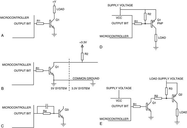
Figure 34.6 Driving bipolar transistors
When the output is low, the transistor turns off. The requirements for driving a bipolar transistor from the output of a microcontroller are:
• Voltage output from the microcontroller must be high enough to turn the transistor on, typically greater than 0.8V.
• Current into the base of the transistor must be high enough to saturate the transistor.
• Current into the base of the transistor must be limited to a value that will avoid damage to the transistor.
• Low-output voltage of the microcontroller output must be low enough to ensure that the transistor turns off. This is typically not a problem unless the output must sink significant current.
The current into the base of the transistor is calculated as:
![]()
(In the figure, R1 is the base resistor.) The logic high voltage is the value of the output voltage for the logic used. It may vary with the load, so a logic output that nominally swings to the supply may deliver less voltage if it cannot supply adequate current. The transistor base-emitter voltage, Vbe, is typically 0.6V to 0.8V.
Whether the transistor can pull its collector close enough to ground to function as a logic output depends on the load and the base drive. The maximum collector current is approximately equal to the base current times the current gain of the transistor, up to the point at which the transistor saturates. A signal transistor might have a gain of 100, so a few mA of base current can switch a few hundred mA of collector current. A large power transistor may only have a gain of 10 or 20, so it is difficult to drive them directly from the microcontroller outputs—there isn’t enough gain to ensure that the transistor is saturated when driving a high-current load. Consequently, driving very high current loads typically requires a signal transistor driving the base of a larger power transistor.
The simplest approach to using bipolar transistors is to set the base current at half or less of the maximum rated base current. If this does not provide sufficient collector current for your application, or if you calculate the required base current and find that it exceeds what the microcontroller can produce, then you are trying to switch too much current. Use another type of driver.
Finally, remember that the gain of transistors tends to vary quite a bit from one lot to the next, so don’t build a circuit that depends on very high gain transistors unless you are willing to sort them in production.
34.6.1 Logic Level Translation
Bipolar transistors provide a convenient means to pass signals between two systems at different supply voltages. Figure 34.6B shows a transistor used to connect a 5V microcontroller and a 3.3V external system. The collector of the transistor is pulled up on the 3.3V system through a resistor.
34.6.2 Switching Speed
One problem with driving bipolar transistors directly from the output of a microcontroller (or other logic) is speed. When the transistor is saturated, the base-emitter junction exhibits a characteristic known as stored charge. This, in effect, acts as a capacitor, making the transistor slow to turn off when the logic input goes low. In addition, the output of the transistor circuit (the collector) does not have an active pull-up to force the output high. Instead, a resistor pulls the output high when the transistor turns off. Consequently, the risetime of the output is dependent on the transistor switching speed and the capacitance in the collector circuit. If the transistor is connected to another board via a long cable, this capacitance can be significant.
The turn-on and turn-off speed of the transistor can be improved with the addition of a capacitor across the base resistor, as shown in Figure 34.6C The capacitor is a low impedance when the logic output is changing states, rapidly charging or discharging the base circuit. A typical value for this capacitor is 220 pF, although larger values may be needed for large transistors.
The collector risetime can be reduced by reducing the value of the pull-up resistor. However, smaller resistor values increase supply current drain and transistor dissipation. Also, a smaller pull-up resistor means more base current is needed to ensure that the transistor will be saturated. These techniques will make a transistor circuit switch faster, but a discrete transistor design will never be as fast as a driver or interface IC designed for a specific application. Bipolar transistors find primary use in controlling currents or voltages beyond the capability of the microcontroller/microprocessor itself.
34.6.3 High-Side Switches
In some cases, you need to pull an output up instead of clamping it to ground. Figure 34.6D shows a PNP transistor used in this way. The PNP is wired with the emitter connected to the positive supply voltage (the NPN had the emitter grounded), so pulling the base toward ground turns the transistor on. The resistor between the base and emitter of the transistor ensures that the base goes all the way to the supply, turning the transistor completely off, in case the microcontroller output doesn’t quite swing all the way.
The same considerations apply as for the NPN transistor in terms of the base current. The base current in this case is at maximum when the microcontroller output is low.
In some cases, you need to supply current from a higher supply voltage than the microcontroller is using. For instance, a 5V or 3.3V microcontroller may need to switch the 12V supply to a motor. Figure 34.6E shows how a PNP and NPN can be used together for this. The NPN transistor isolates the microcontroller from the high voltage on the base of the PNP transistor.
34.7 Driving MOSFETs
Like bipolar transistors, MOSFETs also provide a means to control voltages and currents outside the range of the microcontroller. The simplest MOSFET drive is shown in Figure 34.7A Here, a microcontroller output directly drives the MOSFET gate. When the microcontroller output is high, the MOSFET is turned on and sinks current. When the microcontroller output is low, the MOSFET is turned off. The key points to remember in driving a MOSFET in this way are
• The output voltage of the microcontroller must be greater than the MOSFET gate-to-source threshold voltage or the MOSFET will not turn on. This is more of a problem with 3V logic than with 5V logic, but either logic voltage requires the use of a MOSFET with a logic-level threshold voltage. If necessary, a pull-up resistor can be added to the logic signal to ensure that it goes all the way to the supply voltage.
• The MOSFET has significant gate-to-source and gate-to-drain capacitance, shown as Cgs and Cgd in the figure. Generally, the larger the MOSFET, the greater this capacitance is. If the MOSFET is driving a signal that can have large voltage spikes, such as an inductive load, sufficient voltage can be coupled back into the microcontroller to damage the outputs.
• The MOSFET turn-on time is limited by the speed at which the gate-to-source voltage rises. This in turn is determined by how quickly the microcontroller can charge up the gate-source capacitance. Many microcontroller outputs have very limited output current capability. If the MOSFET turn-on time is too long and the switching frequency is high, the MOSFET will dissipate excessive power as it transitions from cut-off to saturation.
• If a pull-up resistor is needed to ensure adequate turn-on voltage, the turn-on time of the MOSFET will be limited to the risetime of the pull-up resistor in combination with the gate-source capacitance of the MOSFET. Because the current sinking capability of the microcontroller output limits the size of the pull-up resistor, the switching speed of the MOSFET is also limited by the same current sink capability.

Figure 34.7 Driving MOSFET transistors
Many of these problems can be eliminated by using a MOSFET driver IC, as shown in Figure 34.7B In this circuit, a Maxim MAX5048 is used to drive the MOSFET. The MAX5048 provides logic level inputs and can operate on supply voltages up to 12.6V. The MAX5048 has separate sourcing (P-channel) and sinking (N-channel) outputs. In the figure, resistor R1 is not needed. If R1 were not used, the P output and N output would be tied together and to the gate of the FET. R1 in series with the P output limits the rise-time of the gate, and thereby the turn-on time of the FET. If the gate of the FET is connected to the P output instead of to the N output, then R1 will limit the fall time of the gate and thereby the turn-off time of the FET.
34.7.1 High-Side Switching
In some cases, you want to source current instead of sinking current. The simplest way to do this is with a P-channel MOSFET, as shown in Figure 34.7C In this circuit, the MAX5048 is used to drive the P-channel output transistor. Note that the P-channel MOSFET has the source connected to the positive supply and the gate must be driven toward ground to turn the transistor on.
The problem with P-channel MOSFETs is that they tend to be more expensive than equivalent N-channel MOSFETs and they usually have a higher ON resistance, causing the transistor to dissipate more power when turned on. In some applications, the gate-to-source capacitance can couple the load voltage into the MOSFET gate, turning it on when it should be off. This typically occurs with inductive loads or when there is another transistor pulling the load to ground when the P-channel MOSFET is off. For these reasons, N-channel MOSFETs are usually preferred for high-side switching applications.
The primary difficulty in using an N-channel MOSFET for high-side switching is the gate drive voltage. To turn the N-channel MOSFET on, the gate must be driven higher than the source; because the source is connected to the load in a high side application, this means the gate must be driven higher than the positive supply voltage.
In most cases, the MOSFET is used to drive the load from the highest voltage available in the system, so there is no higher voltage available to drive the MOSFET gate. You have two choices in this case: you can use a bootstrap MOSFET driver or you can add a DC-DC converter.
The DC-DC converter is the simplest solution, as shown in Figure 34.7D You add a DC-DC converter to the board and use a MOSFET driver IC. The output of the DC-DC converter must not exceed the maximum gate-source voltage, or the MOSFET may be damaged. In the figure, a DC-DC converter with a 16V output produces the gate drive voltage for a driver IC. The gate of the MOSFET will switch between ground and 16V, and the load will switch between ground and 12V. Note that the gate drive voltage cannot exceed the gate-to-source breakdown voltage, which is typically 18V for a MOSFET.
A bootstrap MOSFET driver IC can also drive a high-side MOSFET, as shown in Figure 34.7E. A bootstrap driver uses a capacitor (external to the IC) that is charged up to the supply voltage when the load is low. If the circuit is being used to drive a high-side switch, with no low-side driver, the capacitor charges through the load. If the circuit is being used to drive a pair of MOSFETs, one providing high-side drive and one providing low-side drive, the capacitor charges through the low-side MOSFET when it is turned on.
When the high-side driver is turned on, the bootstrap capacitor is switched so that it drives the gate of the MOSFET above the supply voltage to turn it on. Typically, the bootstrap capacitor is much larger than the gate-source capacitance of the MOSFET, so the voltage across the capacitor does not drop very far when driving the MOSFET gate. However, once the high-side MOSFET is turned on, there is no longer a charging path for the bootstrap capacitor, so it will eventually discharge. For this reason, bootstrap circuits are normally used in applications in which the MOSFET is continuously switching. If you need to turn the MOSFET on and leave it on, you will need a DC-DC converter or some similar method.
34.8 Reading Negative Voltages
Sometimes you need to read and convert a negative voltage with an ADC that operates only from ground and a positive supply. Sometimes the only way to accomplish this is to use an op-amp, powered from both positive and negative supplies, to shift the signal to a range the ADC can use.
Figure 34.8 shows a simple resistor voltage divider that will accomplish the same thing, with some limitations. In the figure, the input is a sine signal that swings between −2V and +2V, being read by a microcontroller that operates from +5V and ground. Using a voltage divider (R1 and R2) brings the signal within the 0–5V range of the microcontroller ADC input. With the values used in the figure, the signal swing is 1.5V to 3.5V. There are a few limitations on this technique:
• The voltage divider essentially acts as a resistive pull-up to the supply voltage. This may affect the input signal.
• The voltage swing is reduced; in the figure, a 4VP-P signal is reduced to 2V P-P at the microcontroller ADC input.
• Large resistors may be needed to avoid loading the input signal source. Large resistors, coupled with the input capacitance of the microcontroller, limit the speed.
• If the input can occasionally go negative enough to bring the microcontroller input below ground, the microcontroller may be destroyed. The maximum signal excursion must be known, or a diode, as shown in the figure, must be used to clamp the signal to ground.
• The actual voltage produced at the microcontroller input is dependent on both the input signal voltage and the supply voltage. Variations in the supply voltage will affect the ADC reading.

Figure 34.8 Resistive divider for reading negative input signals
34.9 Example Control System
To illustrate some of the principles described in previous chapters, an example control system was developed. This concept system is easy to build and is useful for experimenting with control concepts. Figure 34.9 shows a block diagram of the system. The control system is simulated with an inexpensive lamp coupled to an infrared phototransistor. The lamp and phototransistor are held in place with a length of heatshrink or other opaque tubing.
A PWM circuit is used to control the current through the lamp. The prototype used for the examples here operated at about 14 kHz. An analog control could also be used, with a DAC followed by an op-amp capable of delivering sufficient current to the bulb. The ADC was an 8-bit converter, with an output value of 0 representing 0V and a value of 255 representing 5V.
The system is controlled by a PC, although the same arrangement could be controlled by a microcontroller or single-board computer. Using a PC is less precise than using a more hardware-oriented approach, because the sampling rate in a PC will vary with operating system activity. However, it is close enough to make a useful experimentation tool. For the examples used here, the code was written in Python.
This simple arrangement provides a good simulation of a control system. The lamp filament is, in effect, a heater. The lamp filament does not heat up instantly and the phototransistor is relatively slow, so the combination has many of the characteristics of a real heater or motor arrangement.
In Figure 34.9, R2 is shown with dashed connections. R2 is installed in parallel with R1 to simulate an external load, as will be described later.
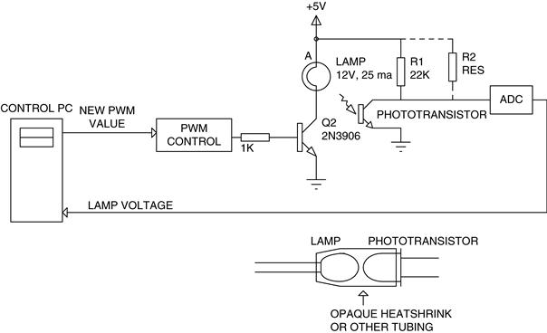
Figure 34.9 Simulation system block diagram
Note that this is a reversed control system—a higher control value results in a lower ADC value because a hotter filament results in more phototransistor current.
Figure 34.10A shows the step response of the system. This waveform was created by starting with a PWM value of 1 (just barely turning the lamp on) and then changing to a PWM value of 250 (almost 100% on) and sampling the resulting voltage from the phototransistor once per millisecond. Note that the lamp has a short delay before it starts heating, then a rapid heating period, then a slower curve as it approaches its final temperature. This data was plotted using Microsoft Excel.
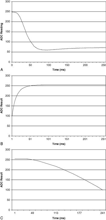
Figure 34.10 Simulation system characterization
Figure 34.10B shows the reverse of the positive step. Here, the PWM value was set to 250 and the output was allowed to settle for one second. The PWM was then turned off and the output was measured once per millisecond. The result is an exponential curve as the lamp filament cools. This asymmetrical characteristic of the system is typical of many real-world environments.
Figure 34.10C shows the characterization of the system with respect to the control value. This curve was made by applying 16 equally spaced control values from 1 to 241, allowing the output to settle, and measuring the ADC result.
34.9.1 On-Off (Bang-Bang) Control
An on-off control is illustrated in Figure 34.11A The setpoint for this example was 100, corresponding to about 1.95Vat the phototransistor collector. Note the oscillation around the setpoint—it ranges from 98 to 112, a range of 0.3 volts, or 15% of the setpoint value. The oscillation is not centered around the setpoint, but is skewed toward the high values. This occurs because the control response is not symmetrical—the filament cools down more quickly than it heats up.

Figure 34.11 On-off control examples
Figure 34.11B shows an on-off control with a setpoint of 150. There is less oscillation at this setpoint; a control system that is not linear across its range will exhibit characteristics like this. Figure 34.11C shows an on-off control with a setpoint of 100 and a sampling interval of 4 ms. Note the size of the oscillation; the sampling interval has a significant effect on the result.
Figure 34.12 shows an on-off control starting with the PWM full on and using a setpoint of 150. Unlike the case that started with the PWM off, there is significant overshoot past the setpoint; the lamp filament cools down more easily than it heats up, so there is more momentum in that direction.

Figure 34.12 On-off control, starting with PWM 100% on
34.9.2 Proportional Control
Figure 34.13A shows a proportional control with a setpoint of 150 (about 2.9 volts) and a gain of 2. Using the input-to-output characterization curve, an offset of 200 was selected for this setpoint. The equation for the control value is

Figure 34.13 Proportional control
Control output = 200 + (ADC value — setpoint) × Gain If control output > 254, control output = 254. If control output < 1, control output = 1.
The last two statements limit the control value to the 8-bit range of the system.
At a gain of 2, the system stabilizes with an output around 145. Figure 34.13B shows a proportional control, but starting at the top of the range (100% PWM) and using a gain of 20. This time the result makes it to the setpoint of 150, but with significant oscillation. Note the overshoot as the signal passes through 150; like the on-off example, this is caused by the asymmetrical nature of the heater and the additional gain. If the gain is reduced, the overshoot can be eliminated, but the result ends up below the setpoint (150). Although a graph is not shown for this condition, at a gain of 10, the waveform overshoots just slightly and then settles down to oscillate between 149 and 150.
Figure 34.13C shows a proportional system with a gain of 10, setpoint of 150, and an offset of 100. The lower offset results in a final result between 157 and 158. As you can see, the gain and offset both affect the final result in a proportional system. However, the proportional control is still better than open-loop control, because an open-loop control value of 100 results in an ADC value of 222 (see the characterization chart).
Figure 34.14 shows the proportional system with a setpoint of 150, gain of 10, and a load of 47K (R2) in parallel with the 22K collector resistor (R1). There is a small overshoot as the output passes 150, then the output settles down to oscillate between 152 and 153. Note that the addition of a load caused a permanent offset in the output—the proportional system was unable to completely compensate for the effects of the added load.
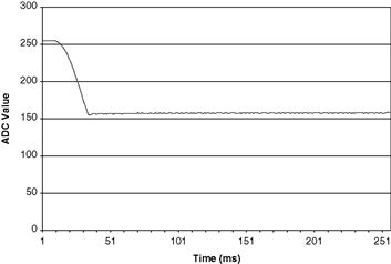
Figure 34.14 Proportional control with load
34.9.3 Pid
Figure 34.15A shows a simple PID control. The parameters are:
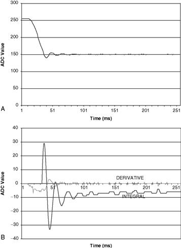
Figure 34.15 PID control with integral and derivative waveforms
To prevent integral windup, the integral is held at zero until the ADC result is within 10% of the setpoint. As you can see, there is a little overshoot and then the output settles down to values of 150 and 151. Figure 34.15B shows the integral and derivative terms. Note that changes (edges) in the integral waveform correspond to a positive and negative transition in the derivative waveform, because the derivative is measuring the amount that the error changed from the previous sample.
Figure 34.16A shows what happens if the derivative gain is set to 40; a high-frequency oscillation occurs, although it is centered on the setpoint. In Figure 34.16B, the derivative gain is set to 2 again, and the integral gain is set to 40. This condition causes an oscillation between about 135 and 172, and at a lower frequency than the oscillation caused by the large derivative value. This is typical of PID control systems—excessive derivative gain and excessive integral gain both cause oscillation, but the oscillation caused by the integral gain is at a lower frequency.

Figure 34.16 PID control with large derivative and integral values
Figure 34.17A shows the following conditions:

Figure 34.17 PID control with load
The result is a very smooth waveform with good control at the setpoint. The waveform in Figure 34.17B uses the same parameters, but adds a 47K resistor (R2) in parallel with the 22K resistor R1. The important thing to note here is that the final value still reaches the setpoint, although there is a “knee” in the waveform around sample 37.
34.9.4 Proportional-Integral Control
Figure 34.18 shows a proportional-integral control only, with proportional gain = 4 and integral gain = 0.1. The waveform overshoots to 140, which is past the value of 145 that was reached with the proportional-only control, but the integral eventually brings the result up to the target value of 150.
Figure 34.18 Proportional-integral control